IDTADC1215S080HN-C18 数据手册
ADC1215S series
Single 12-bit ADC; 65 Msps, 80 Msps, 105 Msps or 125 Msps
with input buffer; CMOS or LVDS DDR digital outputs
Rev. 03 — 2 July 2012
Product data sheet
1. General description
The ADC1215S is a single channel 12-bit Analog-to-Digital Converter (ADC) optimized for
high dynamic performance and low power consumption at sample rates up to 125 Msps.
Pipelined architecture and output error correction ensure the ADC1215S is accurate
enough to guarantee zero missing codes over the entire operating range. Supplied from a
single 3 V source, it can handle output logic levels from 1.8 V to 3.3 V in CMOS mode
because of a separate digital output supply.
The ADC1215S supports the Low Voltage Differential Signalling (LVDS) Double Data
Rate (DDR) output standard. An integrated Serial Peripheral Interface (SPI) allows the
user to easily configure the ADC.
The device also includes a SPI programmable full-scale to allow flexible input voltage
range from 1 V to 2 V (peak-to-peak). With excellent dynamic performance from the
baseband to input frequencies of 170 MHz or more, the ADC1215S is ideal for use in
communications, imaging and medical applications - especially in high Intermediate
Frequency (IF) applications because of the integrated input buffer. The input buffer
ensures that the input impedance remains constant and low and the performance
consistent over a wide frequency range.
2. Features and benefits
SNR, 70 dBFS / SFDR, 86 dBc
Sample rate up to 125 Msps
12-bit pipelined ADC core
Clock input divided by 2 for less jitter
contribution
Integrated input buffer
Flexible input voltage range: 1 V (p-p) to
2 V (p-p)
CMOS or LVDS DDR digital outputs
Pin compatible with the ADC1415S
series, the ADC1015S series and the
ADC1115S125
Input bandwidth, 600 MHz
Power dissipation, 635 mW at 80 Msps,
including analog input buffer
SPI
Duty cycle stabilizer
Fast OuT-of-Range (OTR) detection
Offset binary, two’s complement, gray
code
Power-down and Sleep modes
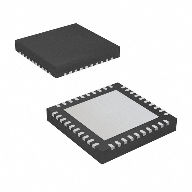
HVQFN40 package
®
�ADC1215S series
Integrated Device Technology
Single 12-bit ADC; input buffer; CMOS or LVDS DDR digital output
3. Applications
Wireless and wired broadband
communications
Portable instrumentation
Imaging systems
Digital predistortion loop, power
amplifier linearization
Spectral analysis
Ultrasound equipment
Software defined radio
4. Ordering information
Table 1.
Ordering information
Type number
fs (Msps) Package
Name
Description
Version
ADC1215S125HN-C1 125
HVQFN40 plastic thermal enhanced very thin quad flat package; no
leads; 40 terminals; body 6 6 0.85 mm
SOT618-6
ADC1215S105HN-C1 105
HVQFN40 plastic thermal enhanced very thin quad flat package; no
leads; 40 terminals; body 6 6 0.85 mm
SOT618-6
ADC1215S080HN-C1 80
HVQFN40 plastic thermal enhanced very thin quad flat package; no
leads; 40 terminals; body 6 6 0.85 mm
SOT618-6
ADC1215S065HN-C1 65
HVQFN40 plastic thermal enhanced very thin quad flat package; no
leads; 40 terminals; body 6 6 0.85 mm
SOT618-6
ADC1215S_SER 3
Product data sheet
© IDT All rights reserved.
Rev. 03 — 2 July 2012
2 of 40
�ADC1215S series
Integrated Device Technology
Single 12-bit ADC; input buffer; CMOS or LVDS DDR digital output
5. Block diagram
SDIO/ODS
CS
SCLK/DFS
ADC1215S
ERROR
CORRECTION AND
DIGITAL
PROCESSING
SPI
OTR
INP
INPUT
BUFFER
S/H
INPUT
STAGE
ADC CORE
12-BIT
PIPELINED
OUTPUT
DRIVERS
INM
OUTPUT
DRIVERS
CLOCK INPUT
STAGE AND DUTY
CYCLE CONTROL
SYSTEM
REFERENCE AND
POWER
MANAGEMENT
CLKP CLKM
VREF
REFB
VCM
SENSE REFT
CMOS:
D11 to D0
or
LVDS DDR:
D10_D11_P
to D0_D1_P
D10_D11_M
to D0_D1_M
CMOS:
DAV
or
LVDS DDR:
DAVP
DAVM
PWD
OE
005aaa140
Fig 1.
Block diagram
ADC1215S_SER 3
Product data sheet
© IDT All rights reserved.
Rev. 03 — 2 July 2012
3 of 40
�ADC1215S series
Integrated Device Technology
Single 12-bit ADC; input buffer; CMOS or LVDS DDR digital output
6. Pinning information
31 DAV
32 n.c.
33 VDDO
34 OGND
35 OTR
36 SCLK/DFS
37 SDIO/ODS
38 CS
39 SENSE
40 VREF
terminal 1
index area
31 DAV
32 n.c.
33 VDDO
34 OGND
35 OTR
36 SCLK/DFS
37 SDIO/ODS
38 CS
terminal 1
index area
39 SENSE
40 VREF
6.1 Pinning
REFB
1
30 n.c.
REFB
1
30 n.c.
REFT
2
29 n.c.
REFT
2
29 n.c.
AGND
3
28 D0_D1_P
AGND
3
28 D0
VCM
4
VCM
4
27 D1
VDDA5V
5
VDDA5V
5
26 D2
AGND
6
AGND
6
25 D3
INM
7
24 D4_D5_P
INM
7
24 D4
INP
8
23 D4_D5_M
INP
8
23 D5
AGND
9
22 D6_D7_P
AGND
9
22 D6
VDDA3V 10
21 D6_D7_M
VDDA3V 10
21 D7
26 D2_D3_P
D8_D9_P 20
D8_D9_M 19
25 D2_D3_M
D10_D11_P 18
PWD 16
OE 15
DEC 14
CLKM 13
Transparent top view
D10_D11_M 17
005aaa141
CLKP 12
VDDA3V 11
D8 20
D9 19
D10 18
D11 17
PWD 16
OE 15
DEC 14
CLKM 13
CLKP 12
VDDA3V 11
ADC1215S
HVQFN40
27 D0_D1_M
ADC1215S
HVQFN40
005aaa142
Transparent top view
Fig 2.
Pin configuration with CMOS digital outputs
selected
Fig 3.
Pin configuration with LVDS/DDR digital
outputs selected
6.2 Pin description
Table 2.
Pin description (CMOS digital outputs)
Symbol
Pin
Type [1]
Description
REFB
1
O
bottom reference
REFT
2
O
top reference
AGND
3
G
analog ground
VCM
4
O
common-mode output voltage
VDDA5V
5
P
5 V analog power supply
AGND
6
G
analog ground
INM
7
I
complementary analog input
INP
8
I
analog input
AGND
9
G
analog ground
VDDA3V
10
P
3 V analog power supply
VDDA3V
11
P
3 V analog power supply
CLKP
12
I
clock input
CLKM
13
I
complementary clock input
DEC
14
O
regulator decoupling node
OE
15
I
output enable, active LOW
PWD
16
I
power down, active HIGH
ADC1215S_SER 3
Product data sheet
© IDT All rights reserved.
Rev. 03 — 2 July 2012
4 of 40
�ADC1215S series
Integrated Device Technology
Single 12-bit ADC; input buffer; CMOS or LVDS DDR digital output
Table 2.
Pin description (CMOS digital outputs) …continued
Symbol
Pin
Type [1]
Description
D11
17
O
data output bit 11 (Most Significant Bit (MSB))
D10
18
O
data output bit 10
D9
19
O
data output bit 9
D8
20
O
data output bit 8
D7
21
O
data output bit 7
D6
22
O
data output bit 6
D5
23
O
data output bit 5
D4
24
O
data output bit 4
D3
25
O
data output bit 3
D2
26
O
data output bit 2
D1
27
O
data output bit 1
D0
28
O
data output bit 0 (Least Significant Bit (LSB))
n.c.
29
-
not connected
n.c.
30
-
not connected
DAV
31
O
data valid output clock
n.c.
32
-
not connected
VDDO
33
P
output power supply
OGND
34
G
output ground
OTR
35
O
out of range
SCLK/DFS
36
I
SPI clock / data format select
SDIO/ODS
37
I/O
SPI data IO / output data standard
CS
38
I
SPI chip select
SENSE
39
I
reference programming pin
VREF
40
I/O
voltage reference input/output
[1]
P: power supply; G: ground; I: input; O: output; I/O: input/output.
Table 3.
Pin description (LVDS/DDR) digital outputs)
Symbol
Pin [1]
Type [2]
Description
D10_D11_M
17
O
differential output data D10 and D11 multiplexed, complement
D10_D11_P
18
O
differential output data D10 and D11 multiplexed, true
D8_D9_M
19
O
differential output data D8 and D9 multiplexed, complement
D8_D9_P
20
O
differential output data D8 and D9 multiplexed, true
D6_D7_M
21
O
differential output data D6 and D7 multiplexed, complement
D6_D7_P
22
O
differential output data D6 and D7 multiplexed, true
D4_D5_M
23
O
differential output data D4 and D5 multiplexed, complement
D4_D5_P
24
O
differential output data D4 and D5 multiplexed, true
D2_D3_M
25
O
differential output data D2 and D3 multiplexed, complement
D2_D3_P
26
O
differential output data D2 and D3 multiplexed, true
D0_D1_M
27
O
differential output data D0 and D1 multiplexed, complement
D0_D1_P
28
O
differential output data D0 and D1 multiplexed, true
n.c.
29
-
not connected
ADC1215S_SER 3
Product data sheet
© IDT All rights reserved.
Rev. 03 — 2 July 2012
5 of 40
�ADC1215S series
Integrated Device Technology
Single 12-bit ADC; input buffer; CMOS or LVDS DDR digital output
Table 3.
Pin description …continued (LVDS/DDR) digital outputs)
Symbol
Pin [1]
Type [2]
n.c.
30
-
not connected
DAVM
31
O
data valid output clock, complement
DAVP
32
O
data valid output clock, true
Description
[1]
Pins 1 to 16 and pins 33 to 40 are the same for both CMOS and LVDS DDR outputs (see Table 2)
[2]
P: power supply; G: ground; I: input; O: output; I/O: input/output.
7. Limiting values
Table 4.
Limiting values
In accordance with the Absolute Maximum Rating System (IEC 60134).
Symbol Parameter
Conditions
Min
Max
Unit
pins D11 to D0 or
pins D10_D11_P to D0_D1_P and
D10_D11_M to D0_D1_M
0.4
+3.9
V
VDDA(3V) analog supply voltage
3V
on pin VDDA3V
0.5
+4.6
V
VDDA(5V) analog supply voltage
5V
on pin VDDA5V
0.5
+6.0
V
output voltage
VO
VDDO
output supply voltage
0.5
+4.6
V
Tstg
storage temperature
55
+125
C
Tamb
ambient temperature
40
+85
C
Tj
junction temperature
-
125
C
8. Thermal characteristics
Table 5.
Symbol
Thermal characteristics
Parameter
Conditions
Rth(j-a)
thermal resistance from junction to ambient
[1]
Rth(j-c)
thermal resistance from junction to case
[1]
[1]
Unit
30.5
K/W
13.3
K/W
Value for 6 layers board in still air with a minimum of 25 thermal vias.
ADC1215S_SER 3
Product data sheet
Typ
© IDT All rights reserved.
Rev. 03 — 2 July 2012
6 of 40
�ADC1215S series
Integrated Device Technology
Single 12-bit ADC; input buffer; CMOS or LVDS DDR digital output
9. Static characteristics
Table 6.
Symbol
Static characteristics[1]
Parameter
Conditions
Min
Typ
Max
Unit
Supplies
VDDA(5V)
analog supply voltage 5 V
4.75
5.0
5.25
V
VDDA(3V)
analog supply voltage 3 V
2.85
3.0
3.4
V
VDDO
output supply voltage
CMOS mode
1.65
1.8
3.6
V
LVDS DDR mode
2.85
3.0
3.6
V
IDDA(5V)
analog supply current 5 V
fclk = 125 Msps;
fi = 70 MHz
-
46
-
mA
IDDA(3V)
analog supply current 3 V
fclk = 125 Msps;
fi = 70 MHz
-
205
-
mA
IDDO
output supply current
CMOS mode;
fclk = 125 Msps;
fi = 70 MHz
-
12
-
mA
LVDS DDR mode:
fclk = 125 Msps;
fi = 70 MHz
-
39
-
mA
ADC1215S125;
analog supply only
-
840
-
mW
ADC1215S105;
analog supply only
-
770
-
mW
ADC1215S080;
analog supply only
-
635
-
mW
ADC1215S065;
analog supply only
-
580
-
mW
Power-down mode
-
2
-
mW
Standby mode
-
40
-
mW
differential clock input voltage
peak-to-peak
-
1.6
-
V
differential clock input voltage
peak
-
3.0
-
V
P
power dissipation
Clock inputs: pins CLKP and CLKM
LVPECL
Vi(clk)dif
SINE wave
Vi(clk)dif
LVCMOS
VIL
LOW-level input voltage
-
-
0.3VDDA(3V)
V
VIH
HIGH-level input voltage
0.7VDDA(3V)
-
-
V
Logic inputs: pins PWD and OE
VIL
LOW-level input voltage
0
-
0.8
V
VIH
HIGH-level input voltage
2
-
VDDA(3V)
V
IIL
LOW-level input current
-
55
-
A
IIH
HIGH-level input current
-
65
-
A
Serial peripheral interface: pins CS, SDIO/ODS, SCLK/DFS
VIL
LOW-level input voltage
0
-
0.3VDDA(3V)
V
VIH
HIGH-level input voltage
0.7VDDA(3V)
-
VDDA(3V)
V
ADC1215S_SER 3
Product data sheet
© IDT All rights reserved.
Rev. 03 — 2 July 2012
7 of 40
�ADC1215S series
Integrated Device Technology
Single 12-bit ADC; input buffer; CMOS or LVDS DDR digital output
Table 6.
Static characteristics[1] …continued
Symbol
Parameter
IIL
Conditions
Min
Typ
Max
Unit
LOW-level input current
10
-
+10
A
IIH
HIGH-level input current
50
-
+50
A
CI
input capacitance
-
4
-
pF
OGND
-
0.2VDDO
V
0.8VDDO
-
VDDO
V
-
3
-
pF
Digital outputs, CMOS mode: pins D11 to D0, OTR, DAV
Output levels, VDDO = 3 V
VOL
LOW-level output voltage
VOH
HIGH-level output voltage
CO
output capacitance
high impedance;
OE = HIGH
Output levels, VDDO = 1.8 V
VOL
LOW-level output voltage
OGND
-
0.2VDDO
V
VOH
HIGH-level output voltage
0.8VDDO
-
VDDO
V
Digital outputs, LVDS mode: pins D10_D11_P to D0_D1_P, D10_D11_M to D0_D1_M, DAVP and DAVM
Output levels, VDDO = 3 V only, Rload = 100
VO(offset)
output offset voltage
output buffer current
set to 3.5 mA
-
1.2
-
V
VO(dif)
differential output voltage
output buffer current
set to 3.5 mA
-
350
-
mV
CO
output capacitance
-
3
-
pF
Analog inputs: pins INP and INM
II
input current
5
-
+5
A
RI
input resistance
-
550
-
CI
input capacitance
VI(cm)
common-mode input voltage
Bi
input bandwidth
VI(dif)
differential input voltage
VINP = VINM
peak-to-peak
-
1.3
-
pF
0.9
1.5
2
V
-
600
-
MHz
1
-
2
V
Common mode output voltage: pin VCM
VO(cm)
common-mode output voltage
-
0.5VDDA(3V)
-
V
IO(cm)
common-mode output current
-
4
-
mA
I/O reference voltage: pin VREF
VVREF
voltage on pin VREF
output
-
0.5 to 1
-
V
input
0.5
-
1
V
ADC1215S_SER 3
Product data sheet
© IDT All rights reserved.
Rev. 03 — 2 July 2012
8 of 40
�ADC1215S series
Integrated Device Technology
Single 12-bit ADC; input buffer; CMOS or LVDS DDR digital output
Table 6.
Symbol
Static characteristics[1] …continued
Parameter
Conditions
Min
Typ
Max
Unit
1.25
0.25
+1.25
LSB
0.25
0.12
+0.25
LSB
Accuracy
INL
integral non-linearity
DNL
differential non-linearity
Eoffset
offset error
-
2
-
mV
EG
gain error
-
0.5
-
%FS
-
54
-
dBc
guaranteed no
missing codes
Supply
PSRR
[1]
power supply rejection ratio
200 mV (p-p) on
VDDA(3V)
Typical values measured at VDDA(3V) = 3 V, VDDO = 1.8 V, VDDA(5V) = 5 V; Tamb = 25 C and CL = 5 pF; minimum and maximum values
are across the full temperature range Tamb = 40 C to +85 C at VDDA(3V) = 3 V, VDDO = 1.8 V, VDDA(5V) = 5 V, VINP VINM = 1 dBFS;
internal reference mode; applied to CMOS and LVDS interface; unless otherwise specified.
ADC1215S_SER 3
Product data sheet
© IDT All rights reserved.
Rev. 03 — 2 July 2012
9 of 40
�xxxxxxxxxxxxxxxxxxxxx xxxxxxxxxxxxxxxxxxxxxxxxxx xxxxxxx x x x xxxxxxxxxxxxxxxxxxxxxxxxxxxxxx xxxxxxxxxxxxxxxxxxx xx xx xxxxx
xxxxxxxxxxxxxxxxxxxxxxxxxxx xxxxxxxxxxxxxxxxxxx xxxxxx xxxxxxxxxxxxxxxxxxxxxxxxxxxxxxxxxxx xxxxxxxxxxxx x x
xxxxxxxxxxxxxxxxxxxxx xxxxxxxxxxxxxxxxxxxxxxxxxxxxxx xxxxx xxxxxxxxxxxxxxxxxxxxxxxxxxxxxxxxxxxxxxxxxxxxxxxxxx xxxxxxxx
xxxxxxxxxxxxxxxxxxxxxxxxx xxxxxxxxxxxxxxxxxxxx xxx
Integrated Device Technology
ADC1215S_SER 3
Product data sheet
10. Dynamic characteristics
10.1 Dynamic characteristics
Table 7.
Symbol
Dynamic characteristics[1]
Parameter
Conditions
ADC1215S065
Min
Typ
ADC1215S080
Max
Min
Typ
ADC1215S105
Max
Min
Typ
ADC1215S125
Max
Min
Typ
Unit
Max
Analog signal processing
2H
Rev. 03 — 2 July 2012
THD
ENOB
SFDR
total harmonic
distortion
effective
number of bits
signal-tonoise ratio
10 of 40
© IDT All rights reserved.
spuriousfree dynamic
range
-
87
-
-
87
-
-
86
-
-
88
-
dBc
fi = 30 MHz
-
86
-
-
86
-
-
86
-
-
87
-
dBc
fi = 70 MHz
-
85
-
-
85
-
-
84
-
-
85
-
dBc
fi = 170 MHz
-
82
-
-
82
-
-
81
-
-
83
-
dBc
fi = 3 MHz
-
86
-
-
86
-
-
85
-
-
87
-
dBc
fi = 30 MHz
-
85
-
-
85
-
-
85
-
-
86
-
dBc
fi = 70 MHz
-
84
-
-
84
-
-
83
-
-
84
-
dBc
fi = 170 MHz
-
81
-
-
81
-
-
80
-
-
82
-
dBc
fi = 3 MHz
-
83
-
-
83
-
-
82
-
-
84
-
dBc
fi = 30 MHz
-
82
-
-
82
-
-
82
-
-
83
-
dBc
fi = 70 MHz
-
81
-
-
81
-
-
80
-
-
81
-
dBc
fi = 170 MHz
-
78
-
-
78
-
-
77
-
-
79
-
dBc
fi = 3 MHz
-
11.3
-
-
11.3
-
-
11.3
-
-
11.3
-
bits
fi = 30 MHz
-
11.3
-
-
11.3
-
-
11.3
-
-
11.2
-
bits
fi = 70 MHz
-
11.2
-
-
11.2
-
-
11.2
-
-
11.2
-
bits
fi = 170 MHz
-
11.1
-
-
11.1
-
-
11.1
-
-
11.1
-
bits
fi = 3 MHz
-
70.0
-
-
69.9
-
-
69.8
-
-
69.6
-
dBFS
fi = 30 MHz
-
69.5
-
-
69.5
-
-
69.5
-
-
69.4
-
dBFS
fi = 70 MHz
-
69.2
-
-
69.2
-
-
69.1
-
-
69.0
-
dBFS
fi = 170 MHz
-
68.8
-
-
68.8
-
-
68.7
-
-
68.6
-
dBFS
fi = 3 MHz
-
86
-
-
86
-
-
85
-
-
87
-
dBc
fi = 30 MHz
-
85
-
-
85
-
-
85
-
-
86
-
dBc
fi = 70 MHz
-
84
-
-
84
-
-
83
-
-
84
-
dBc
fi = 170 MHz
-
81
-
-
81
-
-
80
-
-
82
-
dBc
ADC1215S series
SNR
third harmonic
level
fi = 3 MHz
Single 12-bit ADC; input buffer; CMOS or LVDS DDR digital output
3H
second
harmonic level
�Symbol
Dynamic characteristics[1] …continued
Parameter
Conditions
ADC1215S065
Min
IMD
[1]
Intermodulation distortion
Typ
ADC1215S080
Max
Min
Typ
ADC1215S105
Max
Min
Typ
ADC1215S125
Max
Min
Typ
Integrated Device Technology
ADC1215S_SER 3
Product data sheet
Table 7.
xxxxxxxxxxxxxxxxxxxxx xxxxxxxxxxxxxxxxxxxxxxxxxx xxxxxxx x x x xxxxxxxxxxxxxxxxxxxxxxxxxxxxxx xxxxxxxxxxxxxxxxxxx xx xx xxxxx
xxxxxxxxxxxxxxxxxxxxxxxxxxx xxxxxxxxxxxxxxxxxxx xxxxxx xxxxxxxxxxxxxxxxxxxxxxxxxxxxxxxxxxx xxxxxxxxxxxx x x
xxxxxxxxxxxxxxxxxxxxx xxxxxxxxxxxxxxxxxxxxxxxxxxxxxx xxxxx xxxxxxxxxxxxxxxxxxxxxxxxxxxxxxxxxxxxxxxxxxxxxxxxxx xxxxxxxx
xxxxxxxxxxxxxxxxxxxxxxxxx xxxxxxxxxxxxxxxxxxxx xxx
Unit
Max
fi = 3 MHz
-
89
-
-
89
-
-
88
-
-
89
-
dBc
fi = 30 MHz
-
88
-
-
88
-
-
88
-
-
88
-
dBc
fi = 70 MHz
-
87
-
-
87
-
-
86
-
-
86
-
dBc
fi = 170 MHz
-
84
-
-
85
-
-
83
-
-
84
-
dBc
Typical values measured at VDDA(3V) = 3 V, VDDO = 1.8 V, VDDA(5V) = 5 V; Tamb = 25 C and CL = 5 pF; minimum and maximum values are across the full temperature range
Tamb = 40 C to +85 C at VDDA(3V) = 3 V, VDDO = 1.8 V, VDDA(5V) = 5 V, VINP VINM = 1 dBFS; internal reference mode; applied to CMOS and LVDS interface; unless otherwise
specified.
ADC1215S series
11 of 40
© IDT All rights reserved.
Single 12-bit ADC; input buffer; CMOS or LVDS DDR digital output
Rev. 03 — 2 July 2012
�xxxxxxxxxxxxxxxxxxxxx xxxxxxxxxxxxxxxxxxxxxxxxxx xxxxxxx x x x xxxxxxxxxxxxxxxxxxxxxxxxxxxxxx xxxxxxxxxxxxxxxxxxx xx xx xxxxx
xxxxxxxxxxxxxxxxxxxxxxxxxxx xxxxxxxxxxxxxxxxxxx xxxxxx xxxxxxxxxxxxxxxxxxxxxxxxxxxxxxxxxxx xxxxxxxxxxxx x x
xxxxxxxxxxxxxxxxxxxxx xxxxxxxxxxxxxxxxxxxxxxxxxxxxxx xxxxx xxxxxxxxxxxxxxxxxxxxxxxxxxxxxxxxxxxxxxxxxxxxxxxxxx xxxxxxxx
xxxxxxxxxxxxxxxxxxxxxxxxx xxxxxxxxxxxxxxxxxxxx xxx
Table 8.
Symbol
Integrated Device Technology
ADC1215S_SER 3
Product data sheet
10.2 Clock and digital output timing
Clock and digital output timing characteristics[1]
Parameter
Conditions
ADC1410S065
Min
Typ
ADC1410S080
Max
Min
Typ
ADC1410S105
Max
Min
Typ
ADC1410S125
Max
Min
Typ
Unit
Max
Clock timing input: pins CLKP and CLKM
fclk
clock frequency
40
-
65
60
-
80
75
-
105
100
-
125
MHz
tlat(data)
data latency
time
-
13.5
-
-
13.5
-
-
13.5
-
-
13.5
-
clock
cycles
clk
clock duty cycle DCS_EN = 1
30
50
70
30
50
70
30
50
70
30
50
70
%
DCS_EN = 0
45
50
55
45
50
55
45
50
55
45
50
55
%
sampling delay
time
-
0.8
-
-
0.8
-
-
0.8
-
-
0.8
-
ns
twake
wake-up time
-
76
-
-
76
-
-
76
-
-
76
-
s
14.9
16.4
11.9
12.9
14.4
8.0
10.8
12.4
8.2
9.7
11.3
ns
CMOS Mode timing output: pins D11 to D0 and DAV
Rev. 03 — 2 July 2012
tPD
propagation
delay
tsu
set-up time
th
hold time
tr
rise time
DATA
13.6
DAV
DATA
[2]
DAV
tf
fall time
DATA
[2]
-
4.2
-
-
3.6
-
-
3.3
-
-
3.4
-
ns
-
12.5
-
-
9.8
-
-
6.8
-
-
5.6
-
ns
-
3.4
-
-
3.3
-
-
3.1
-
-
2.8
-
ns
0.39
-
2.4
0.39
-
2.4
0.39
-
2.4
0.39
-
2.4
ns
0.26
-
2.4
0.26
-
2.4
0.26
-
2.4
0.26
-
2.4
ns
0.19
-
2.4
0.19
-
2.4
0.19
-
2.4
0.19
-
2.4
ns
ADC1215S series
12 of 40
© IDT All rights reserved.
Single 12-bit ADC; input buffer; CMOS or LVDS DDR digital output
td(s)
�Symbol
Clock and digital output timing characteristics[1] …continued
Parameter
Conditions
ADC1410S065
Min
Typ
ADC1410S080
Max
Min
Typ
ADC1410S105
Max
Min
Typ
ADC1410S125
Max
Min
Typ
Integrated Device Technology
ADC1215S_SER 3
Product data sheet
Table 8.
xxxxxxxxxxxxxxxxxxxxx xxxxxxxxxxxxxxxxxxxxxxxxxx xxxxxxx x x x xxxxxxxxxxxxxxxxxxxxxxxxxxxxxx xxxxxxxxxxxxxxxxxxx xx xx xxxxx
xxxxxxxxxxxxxxxxxxxxxxxxxxx xxxxxxxxxxxxxxxxxxx xxxxxx xxxxxxxxxxxxxxxxxxxxxxxxxxxxxxxxxxx xxxxxxxxxxxx x x
xxxxxxxxxxxxxxxxxxxxx xxxxxxxxxxxxxxxxxxxxxxxxxxxxxx xxxxx xxxxxxxxxxxxxxxxxxxxxxxxxxxxxxxxxxxxxxxxxxxxxxxxxx xxxxxxxx
xxxxxxxxxxxxxxxxxxxxxxxxx xxxxxxxxxxxxxxxxxxxx xxx
Unit
Max
LVDS DDR mode timing output: pins D10_D11_P to D0_D1_P, D10_D11_M to D0_D1_M, DAVP and DAVM
tPD
propagation
delay
tsu
set-up time
th
hold time
tr
rise time
DATA
3.3
5.1
7.6
2.9
4.6
7.1
2.5
4.2
6.8
2.2
4.0
6.6
ns
DAV
-
2.8
-
-
2.5
-
-
2.3
-
-
2.2
-
ns
-
5.4
-
-
4.1
-
-
2.6
-
-
1.9
-
ns
DATA
[3]
DAV
tf
fall time
DATA
[3]
-
2.2
-
-
2.0
-
-
1.8
-
-
1.7
-
ns
0.5
-
5
0.5
-
5
0.5
-
5
0.5
-
5
ns
0.18
-
2.4
0.18
-
2.4
0.18
-
2.4
0.18
-
2.4
ns
0.15
-
1.6
0.15
-
1.6
0.15
-
1.6
0.15
-
1.6
ns
Typical values measured at VDDA(3V) = 3 V, VDDO = 1.8 V, VDDA(5V) = 5 V; Tamb = 25 C and CL = 5 pF; minimum and maximum values are across the full temperature range
Tamb = 40 C to +85 C at VDDA(3V) = 3 V, VDDO = 1.8 V, VDDA(5V) = 5 V, VINP VINM = 1 dBFS; internal reference mode; applied to CMOS and LVDS interface; unless otherwise
specified.
[2]
Measured between 20 % to 80 % of VDDO.
[3]
Rise time measured from 50 mV to +50 mV; fall time measured from +50 mV to 50 mV.
ADC1215S series
13 of 40
© IDT All rights reserved.
Single 12-bit ADC; input buffer; CMOS or LVDS DDR digital output
Rev. 03 — 2 July 2012
[1]
�ADC1215S series
Integrated Device Technology
Single 12-bit ADC; input buffer; CMOS or LVDS DDR digital output
N+1
N
td(s)
N+2
tclk
CLKP
CLKM
tPD
(N − 14)
(N − 13)
(N − 12)
(N − 11)
DATA
tsu
tPD
th
DAV
tclk
005aaa060
Fig 4.
CMOS mode timing
N+1
N
td(s)
N+2
tclk
CLKP
CLKM
tPD
(N − 14)
(N − 13)
(N − 12)
(N − 11)
Dx_Dx + 1_P
Dx
Dx + 1
Dx
Dx + 1
Dx
Dx + 1
Dx
Dx + 1
Dx
Dx + 1
Dx_Dx + 1_M
tsu th tsu th
tPD
DAVP
DAVM
tclk
Fig 5.
LDVS DDR mode timing
ADC1215S_SER 3
Product data sheet
005aaa061
© IDT All rights reserved.
Rev. 03 — 2 July 2012
14 of 40
�ADC1215S series
Integrated Device Technology
Single 12-bit ADC; input buffer; CMOS or LVDS DDR digital output
10.3 SPI timings
Table 9.
SPI timings characteristics[1]
Symbol
Parameter
tw(SCLK)
SCLK pulse width
tw(SCLKH)
SCLK HIGH pulse width
-
16
-
ns
tw(SCLKL)
SCLK LOW pulse width
-
16
-
ns
tsu
set-up time
data to SCLK HIGH
-
5
-
ns
CS to SCLK HIGH
-
5
-
ns
data to SCLK HIGH
-
2
-
ns
CS to SCLK HIGH
-
2
-
ns
-
25
-
MHz
hold time
th
fclk(max)
[1]
Conditions
maximum clock frequency
Min
Typ
Max
Unit
-
40
-
ns
Typical values measured at VDDA(3V) = 3 V, VDDO = 1.8 V, VDDA(5V) = 5 V, Tamb = 25 C and CL = 5 pF;
minimum and maximum values are across the full temperature range Tamb = 40 C to +85 C at
VDDA = 3 V, VDDO = 1.8 V.
tsu
tsu
th
CS
tw(SCLKL)
th
tw(SCLKH)
tw(SCLK)
SCLK
SDIO
R/W
W1
W0
A12
A11
D2
D1
D0
005aaa065
Fig 6.
SPI timing
ADC1215S_SER 3
Product data sheet
© IDT All rights reserved.
Rev. 03 — 2 July 2012
15 of 40
�ADC1215S series
Integrated Device Technology
Single 12-bit ADC; input buffer; CMOS or LVDS DDR digital output
10.4 Typical characteristics
001aam616
100
SFDR
(dBc)
001aam615
80
(1)
SNR
(dBFS)
(1)
80
60
60
(2)
(2)
40
40
20
20
0
0
10
30
50
70
δ (%)
90
10
T = 25 C; VDD = 3 V; fi = 170 MHz; fs = 125 Msps
(1) DCS on
(2) DCS off
(2) DCS off
Spurious-free dynamic range as a function of
duty cycle ()
001aam617
92
SFDR
(dBc)
88
50
70
δ (%)
90
T = 25 C; VDD = 3 V; fi = 170 MHz; fs = 125 Msps
(1) DCS on
Fig 7.
30
Fig 8.
Signal-to-noise ratio as a function of duty
cycle ()
001aam618
80
(1)
SNR
(dBFS)
(2)
60
(1)
(2)
(3)
(3)
84
40
80
20
10
30
50
70
δ (%)
90
(1) Tamb = 40 C/typical supply voltages
10
30
50
70
(2) Tamb = +25 C/typical supply voltages
(2) Tamb = +25 C/typical supply voltages
(3) Tamb = +90 C/typical supply voltages
Spurious-free dynamic range as a function of
duty cycle ()
Fig 10. Signal-to-noise ratio as a function of duty
cycle ()
ADC1215S_SER 3
Product data sheet
90
(1) Tamb = 40 C/typical supply voltages
(3) Tamb = +90 C/typical supply voltages
Fig 9.
δ (%)
© IDT All rights reserved.
Rev. 03 — 2 July 2012
16 of 40
�ADC1215S series
Integrated Device Technology
Single 12-bit ADC; input buffer; CMOS or LVDS DDR digital output
001aam659
90
001aam660
75
SFDR
(dBc)
SNR
(dBFS)
86
73
82
71
78
69
74
67
70
65
0
0.5
1.0
1.5
2.0
2.5
3.0
3.5
0
0.5
1.0
1.5
2.0
2.5
VI(cm) (V)
Fig 11. Spurious-free dynamic range as a function of
common-mode input voltage (Vi(cm))
3.0
3.5
VI(cm) (V)
Fig 12. Signal-to-noise ratio as a function of
common-mode input voltage (Vi(cm))
11. Application information
11.1 Device control
The ADC1215S can be controlled via the Serial Peripheral Interface (SPI control mode) or
directly via the I/O pins (Pin control mode).
11.1.1 SPI and Pin control modes
The device enters Pin control mode at power-up, and remains in this mode as long as pin
CS is held HIGH. In Pin control mode, the SPI pins SDIO, CS and SCLK are used as
static control pins.
SPI control mode is enabled by forcing pin CS LOW. Once SPI control mode has been
enabled, the device remains in this mode. The transition from Pin control mode to SPI
control mode is illustrated in Figure 13.
CS
SCLK/DFS
SDIO/ODS
Pin control mode
Data format
two's complement
SPI control mode
Data format
offset binary
LVDS DDR
CMOS
R/W
W1
W0
A12
005aaa039
Fig 13. Control mode selection
When the device enters SPI control mode, the output data standard and data format are
determined by the level on pin SDIO as soon as a transition is triggered by a falling edge
on CS.
ADC1215S_SER 3
Product data sheet
© IDT All rights reserved.
Rev. 03 — 2 July 2012
17 of 40
�ADC1215S series
Integrated Device Technology
Single 12-bit ADC; input buffer; CMOS or LVDS DDR digital output
11.1.2 Operating mode selection
The active ADC1215S operating mode (Power-up, Power-down or Sleep) can be selected
via the SPI interface (see Figure 24) or using pins PWD and OE in Pin control mode, as
described in Table 10.
Table 10.
Operating mode selection via pin PWD and OE
Pin PWD
Pin OE
Operating mode
Output high-Z
0
0
Power-up
no
0
1
Power-up
yes
1
0
Sleep
yes
1
1
Power-down
yes
11.1.3 Selecting the output data standard
The output data standard (CMOS or LVDS DDR) can be selected via the SPI interface
(see Table 23) or using pin ODS in Pin control mode. LVDS DDR is selected when ODS is
HIGH, otherwise CMOS is selected.
11.1.4 Selecting the output data format
The output data format can be selected via the SPI interface (offset binary, two’s
complement or gray code; see Table 23) or using pin DFS in Pin control mode (offset
binary or two’s complement). Offset binary is selected when DFS is LOW. When DFS is
HIGH, two’s complement is selected.
11.2 Analog inputs
11.2.1 Input stage
The analog input of the ADC1215S supports a differential or a single-ended input drive.
Optimal performance is achieved using differential inputs. The ADC inputs are internally
biased and need to be decoupled.
The full-scale analog input voltage range is configurable between 1 V (p-p) and 2 V (p-p)
via a programmable internal reference (see Section 11.3 and Table 21).
The equivalent circuit of the input buffer followed by the Sample and Hold (S/H) input
stage, including ElectroStatic Discharge (ESD) protection and circuit and package
parasitics, is shown in Figure 14.
ADC1215S_SER 3
Product data sheet
© IDT All rights reserved.
Rev. 03 — 2 July 2012
18 of 40
�ADC1215S series
Integrated Device Technology
Single 12-bit ADC; input buffer; CMOS or LVDS DDR digital output
package
ESD
parasitics
switch
INP
Ron = 15 Ω
8
internal
clock
4 pF
sampling
capacitor
INPUT
BUFFER
switch
INM
Ron = 15 Ω
7
internal
clock
4 pF
sampling
capacitor
005aaa107
Fig 14. Input sampling circuit and input buffer
The integrated input buffer offers the following advantages:
• The kickback effect is avoided - the charge injection and glitches generated by the
S/H input stage are isolated from the input circuitry, so there is no need for additional
filtering.
• The input capacitance is very low and constant over a wide frequency range, which
makes the ADC1215S easy to drive.
The sample phase occurs when the internal clock (derived from the clock signal on pin
CLKP/CLKM) is HIGH. The voltage is then held on the sampling capacitors. When the
clock signal goes LOW, the stage enters the hold phase and the voltage information is
transmitted to the ADC core.
ADC1215S_SER 3
Product data sheet
© IDT All rights reserved.
Rev. 03 — 2 July 2012
19 of 40
�ADC1215S series
Integrated Device Technology
Single 12-bit ADC; input buffer; CMOS or LVDS DDR digital output
11.2.2 Transformer
The configuration of the transformer circuit is determined by the input frequency. The
configuration shown in Figure 15 would be suitable for a baseband application.
ADT1-1WT
Analog
input
100 nF
100 nF
INP
50 Ω
100 nF
100 nF
INM
VCM
100 nF
100 nF
005aaa108
Fig 15. Single transformer configuration suitable for baseband applications
The configuration shown in Figure 16 is recommended for high frequency applications. In
both cases, the choice of transformer is a compromise between cost and performance.
ADT1-1WT
Analog
input
100 nF
ADT1-1WT
100 nF
INP
50 Ω
100 Ω
50 Ω
100 nF
INM
VCM
100 nF
100 nF
100 nF
005aaa109
Fig 16. Dual transformer configuration suitable for high intermediate frequency
application
ADC1215S_SER 3
Product data sheet
© IDT All rights reserved.
Rev. 03 — 2 July 2012
20 of 40
�ADC1215S series
Integrated Device Technology
Single 12-bit ADC; input buffer; CMOS or LVDS DDR digital output
11.3 System reference and power management
11.3.1 Internal/external references
The ADC1215S has a stable and accurate built-in internal reference voltage to adjust the
ADC full-scale. This reference voltage can be set internally via SPI or with pins VREF and
SENSE (programmable in 1 dB steps between 0 dB and 6 dB via control bits
INTREF[2:0] when bit INTREF_EN = logic 1; see Table 21). See Figure 18 to Figure 21.
The equivalent reference circuit is shown in Figure 17. External reference is also possible
by providing a voltage on pin VREF as described in Figure 20.
REFT
REFERENCE
AMP
REFB
VREF
EXT_ref
EXT_ref
BUFFER
BANDGAP
REFERENCE
ADC CORE
SENSE
SELECTION
LOGIC
005aaa164
Fig 17. Reference equivalent schematic
If bit INTREF_EN is set to logic 0, the reference voltage is determined either internally or
externally as detailed in Table 11.
Table 11.
Reference selection
Selection
SPI bit
INTREF_EN
SENSE pin
VREF pin
Full-scale (p-p)
internal
(Figure 18)
0
AGND
330 pF capacitor to AGND
2V
internal
(Figure 19)
0
pin VREF connected to pin SENSE and
via a 330 pF capacitor to AGND
external
(Figure 20)
0
VDDA(3V)
external voltage between
0.5 V and 1 V[1]
1 V to 2 V
internal via SPI
(Figure 21)
1
pin VREF connected to pin SENSE and
via 330 pF capacitor to AGND
1 V to 2 V
[1]
The voltage on pin VREF is doubled internally to generate the internal reference voltage.
ADC1215S_SER 3
Product data sheet
1V
© IDT All rights reserved.
Rev. 03 — 2 July 2012
21 of 40
�ADC1215S series
Integrated Device Technology
Single 12-bit ADC; input buffer; CMOS or LVDS DDR digital output
VREF
VREF
330 pF
330
pF
REFERENCE
EQUIVALENT
SCHEMATIC
REFERENCE
EQUIVALENT
SCHEMATIC
SENSE
SENSE
005aaa117
005aaa116
Fig 18. Internal reference, 2 V (p-p) full-scale
Fig 19. Internal reference, 1 V (p-p) full-scale
VREF
V
0.1 μF
VREF
330 pF
REFERENCE
EQUIVALENT
SCHEMATIC
REFERENCE
EQUIVALENT
SCHEMATIC
SENSE
VDDA
SENSE
005aaa119
005aaa118
Fig 20. External reference, 1 V (p-p) to 2 V (p-p)
full-scale
Fig 21. Internal reference via SPI, 1 V (p-p) to 2 V (p-p)
full-scale
Figure 18 to Figure 21 illustrate how to connect the SENSE and VREF pins to select the
required reference voltage source.
11.3.2 Programmable full-scale
The full-scale is programmable between 1 V (peak-to-peak) to 2 V (peak-to-peak)
(see Table 12).
Table 12.
Reference SPI gain control
INTREF
Gain
Full-scale (p-p)
000
0 dB
2V
001
1 dB
1.78 V
010
2 dB
1.59 V
011
3 dB
1.42 V
100
4 dB
1.26 V
101
5 dB
1.12 V
110
6 dB
1V
111
reserved
x
11.3.3 Common-mode output voltage (VO(cm))
A 0.1 F filter capacitor should be connected between pin VCM and ground.
11.3.4 Biasing
The common-mode input voltage (VI(cm)) on pins INP and INM is set internally. The input
buffer bias current can be set to one of three levels (high, medium or low) via the SPI
(see Table 22).
ADC1215S_SER 3
Product data sheet
© IDT All rights reserved.
Rev. 03 — 2 July 2012
22 of 40
�ADC1215S series
Integrated Device Technology
Single 12-bit ADC; input buffer; CMOS or LVDS DDR digital output
11.4 Clock input
11.4.1 Drive modes
The ADC1215S can be driven differentially (LVPECL). It can also be driven by a
single-ended Low Voltage Complementary Metal Oxide Semiconductor (LVCMOS) signal
connected to pin CLKP (pin CLKM should be connected to ground via a capacitor) or
CLKM (pin CLKP should be connected to ground via a capacitor).
CLKP
LVCMOS
clock input
CLKP
CLKM
LVCMOS
clock input
005aaa174
CLKM
005aaa053
a. Rising edge LVCMOS
b. Falling edge LVCMOS
Fig 22. LVCMOS single-ended clock input
Sine
clock input
CLKP
Sine
clock input
CLKP
CLKM
CLKM
005aaa173
005aaa054
a. Sine clock input
b. Sine clock input (with transformer)
CLKP
LVPECL
clock input
CLKM
005aaa172
c. LVPECL clock input
Fig 23. Differential clock input
ADC1215S_SER 3
Product data sheet
© IDT All rights reserved.
Rev. 03 — 2 July 2012
23 of 40
�ADC1215S series
Integrated Device Technology
Single 12-bit ADC; input buffer; CMOS or LVDS DDR digital output
11.4.2 Equivalent input circuit
The equivalent circuit of the input clock buffer is shown in Figure 24. The common-mode
voltage of the differential input stage is set via internal 5 k resistors.
Package
ESD
Parasitics
CLKP
Vcm(clk)
SE_SEL
SE_SEL
5 kΩ
5 kΩ
CLKM
005aaa056
Vcm(clk) = common-mode voltage of the differential input stage.
Fig 24. Equivalent input circuit
Single-ended or differential clock inputs can be selected via the SPI interface (see
Table 20). If single-ended is enabled, the input pin (CLKM or CLKP) is selected via control
bit SE_SEL.
If single-ended is implemented without setting bit SE_SEL to the appropriate value, the
unused pin should be connected to ground via a capacitor.
11.4.3 Duty cycle stabilizer
The duty cycle stabilizer can improve the overall performances of the ADC by
compensating the duty cycle of the input clock signal. When the duty cycle stabilizer is
active (bit DCS_EN = logic 1; see Table 20), the circuit can handle signals with duty
cycles of between 30 % and 70 % (typical). When the duty cycle stabilizer is disabled
(DCS_EN = logic 0), the input clock signal should have a duty cycle of between 45 % and
55 %.
11.4.4 Clock input divider
The ADC1215S contains an input clock divider that divides the incoming clock by a factor
of 2 (when bit CLKDIV = logic 1; see Table 20). This feature allows the user to deliver a
higher clock frequency with better jitter performance, leading to a better SNR result once
acquisition has been performed.
ADC1215S_SER 3
Product data sheet
© IDT All rights reserved.
Rev. 03 — 2 July 2012
24 of 40
�ADC1215S series
Integrated Device Technology
Single 12-bit ADC; input buffer; CMOS or LVDS DDR digital output
11.5 Digital outputs
11.5.1 Digital output buffers: CMOS mode
The digital output buffers can be configured as CMOS by setting bit LVDS_CMOS to
logic 0 (see Table 23).
Each digital output has a dedicated output buffer. The equivalent circuit of the CMOS
digital output buffer is shown in Figure 25. The buffer is powered by a separate
OGND/VDDO to ensure 1.8 V to 3.3 V compatibility and is isolated from the ADC core.
Each buffer can be loaded by a maximum of 10 pF.
VDDO
Parasitics
LOGIC
DRIVER
ESD
Package
50 Ω
Dx
OGND
005aaa057
Fig 25. CMOS digital output buffer
The output resistance is 50 and is the combination of the an internal resistor and the
equivalent output resistance of the buffer. There is no need for an external damping
resistor. The drive strength of both data and DAV buffers can be programmed via the SPI
in order to adjust the rise and fall times of the output digital signals (see Table 30):
ADC1215S_SER 3
Product data sheet
© IDT All rights reserved.
Rev. 03 — 2 July 2012
25 of 40
�ADC1215S series
Integrated Device Technology
Single 12-bit ADC; input buffer; CMOS or LVDS DDR digital output
11.5.2 Digital output buffers: LVDS DDR mode
The digital output buffers can be configured as LVDS DDR by setting bit LVDS_CMOS to
logic 1 (see Table 23).
VDDO
3.5 mA
typ
−
+
DxP/Dx + 1P
100 Ω
RECEIVER
DxM/Dx + 1M
−
+
OGND
005aaa058
Fig 26. LVDS DDR digital output buffer - externally terminated
Each output should be terminated externally with a 100 resistor (typical) at the receiver
side (Figure 26) or internally via SPI control bits LVDS_INT_TER[2:0] (see Figure 27 and
Table 32).
VDDO
3.5 mA
typ
−
+
DxP/Dx + 1P
100 Ω
RECEIVER
DxM/Dx + 1M
+
−
OGND
005aaa059
Fig 27. LVDS DDR digital output buffer - internally terminated
The default LVDS DDR output buffer current is set to 3.5 mA. It can be programmed via
the SPI (bits DAVI[1:0] and DATAI[1:0]; see Table 31) in order to adjust the output logic
voltage levels.
Table 13.
LVDS DDR output register 2
LVDS_INT_TER[2:0]
Resistor value ()
000
no internal termination
001
300
010
180
011
110
100
150
ADC1215S_SER 3
Product data sheet
© IDT All rights reserved.
Rev. 03 — 2 July 2012
26 of 40
�ADC1215S series
Integrated Device Technology
Single 12-bit ADC; input buffer; CMOS or LVDS DDR digital output
Table 13.
LVDS DDR output register 2 …continued
LVDS_INT_TER[2:0]
Resistor value ()
101
100
110
81
111
60
11.5.3 DAta Valid (DAV) output clock
A data valid output clock signal (DAV) is provided that can be used to capture the data
delivered by the ADC1215S. Detailed timing diagrams for CMOS and LVDS DDR modes
are provided in Figure 4 and Figure 5 respectively.
11.5.4 Out-of-Range (OTR)
An out-of-range signal is provided on pin OTR. The latency of OTR is fourteen clock
cycles. The OTR response can be speeded up by enabling Fast OTR
(bit FASTOTR = logic 1; see Table 29). In this mode, the latency of OTR is reduced to only
four clock cycles. The Fast OTR detection threshold (below full-scale) can be
programmed via bits FASTOTR_DET[2:0].
Table 14.
Fast OTR register
FASTOTR_DET[2:0]
Detection level (dB)
000
20.56
001
16.12
010
11.02
011
7.82
100
5.49
101
3.66
110
2.14
111
0.86
11.5.5 Digital offset
By default, the ADC1215S delivers output code that corresponds to the analog input.
However it is possible to add a digital offset to the output code via the SPI (bits
DIG_OFFSET[5:0]; see Table 25).
11.5.6 Test patterns
For test purposes, the ADC1215S can be configured to transmit one of a number of
predefined test patterns (via bits TESTPAT_SEL[2:0]; see Table 26). A custom test pattern
can be defined by the user (TESTPAT_USER; see is transmitted regardless of the analog
input.
11.5.7 Output codes versus input voltage
Table 15.
Output codes
VINP VINM
Offset binary
Two’s complement
OTR pin
< 1
0000 0000 0000
1000 0000 0000
1
1.0000000
0000 0000 0000
1000 0000 0000
0
0,9995117
0000 0000 0001
1000 0000 0001
0
ADC1215S_SER 3
Product data sheet
© IDT All rights reserved.
Rev. 03 — 2 July 2012
27 of 40
�ADC1215S series
Integrated Device Technology
Single 12-bit ADC; input buffer; CMOS or LVDS DDR digital output
Table 15.
Output codes
VINP VINM
Offset binary
Two’s complement
OTR pin
0.9990234
0000 0000 0010
1000 0000 0010
0
0.9985352
0000 0000 0011
1000 0000 0011
0
0.9980469
0000 0000 0100
1000 0000 0100
0
....
....
....
0
0.0009766
0111 1111 1110
1111 1111 1110
0
0.0004883
0111 1111 1111
1111 1111 1111
0
0.0000000
1000 0000 0000
0000 0000 0000
0
+0.0004883
1000 0000 0001
0000 0000 0001
0
+0.0009766
1000 0000 0010
0000 0000 0010
0
....
....
....
0
+0.9980469
1111 1111 1011
0111 1111 1011
0
+0.9985352
1111 1111 1100
0111 1111 1100
0
+0.9990234
1111 1111 1101
0111 1111 1101
0
+0.9995117
1111 1111 1110
0111 1111 1110
0
+1.0000000
1111 1111 1111
0111 1111 1111
0
> +1
1111 1111 1111
0111 1111 1111
1
11.6 Serial Peripheral Interface (SPI)
11.6.1 Register description
The ADC1215S serial interface is a synchronous serial communications port that allows
easy interfacing with many commonly-used microprocessors. It provides access to the
registers that control the operation of the chip.
This interface is configured as a 3-wire type (SDIO as bidirectional pin)
Pin SCLK is the serial clock input and CS is the chip select pin.
Each read/write operation is initiated by a LOW level on CS. A minimum of three bytes is
transmitted (two instruction bytes and at least one data byte). The number of data bytes is
determined by the value of bits W1 and W2 (see Table 17).
Table 16.
Instruction bytes for the SPI
MSB
LSB
Bit
7
6
5
4
3
2
1
0
Description
R/W[1]
W1[2]
W0[2]
A12
A11
A10
A9
A8
A7
A6
A5
A4
A3
A2
A1
A0
[1]
Bit R/W indicates whether it is a read (logic_1) or a write (logic_0) operation.
[2]
Bits W1 and W0 indicate the number of bytes to be transferred after the instruction byte (see Table 17).
ADC1215S_SER 3
Product data sheet
© IDT All rights reserved.
Rev. 03 — 2 July 2012
28 of 40
�ADC1215S series
Integrated Device Technology
Single 12-bit ADC; input buffer; CMOS or LVDS DDR digital output
Table 17.
Number of data bytes to be transferred after the instruction bytes
W1
W0
Number of bytes transmitted
0
0
1 byte
0
1
2 bytes
1
0
3 bytes
1
1
4 bytes or more
Bits A12 to A0 indicate the address of the register being accessed. In the case of a
multiple byte transfer, this address is the first register to be accessed. An address counter
is increased to access subsequent addresses.
The steps involved in a data transfer are as follows:
1. A falling edge on CS in combination with a rising edge on SCLK determine the start of
communications.
2. The first phase is the transfer of the 2-byte instruction.
3. The second phase is the transfer of the data which can vary in length but is always a
multiple of 8 bits. The MSB is always sent first (for instruction and data bytes).
4. A rising edge on CS indicates the end of data transmission.
CS
SCLK
SDIO
R/W W1
W0
A12 A11 A10
A9
A8
A7
A6
A5
A4
A3
A2
A1
A0
D7
D6
D5
Instruction bytes
D4
D3
D2
Register N (data)
D1
D0
D7
D6
D5
D4
D3
D2
D1
D0
Register N + 1 (data)
005aaa062
Fig 28. SPI mode timing
11.6.2 Default modes at start-up
During circuit initialization it does not matter which output data standard has been
selected. At power-up, the device enters Pin control mode.
A falling edge on CS triggers a transition to SPI control mode. When the ADC1215S
enters SPI control mode, the output data standard (CMOS/LVDS DDR) is determined by
the level on pin SDIO (see Figure 29). Once in SPI control mode, the output data standard
can be changed via bit LVDS/CMOS in Table 23.
When the ADC1215S enters SPI control mode, the output data format (two’s complement
or offset binary) is determined by the level on pin SCLK (gray code can only be selected
via the SPI). Once in SPI control mode, the output data format can be changed via bit
DATA_FORMAT[1:0] in Table 23.
ADC1215S_SER 3
Product data sheet
© IDT All rights reserved.
Rev. 03 — 2 July 2012
29 of 40
�ADC1215S series
Integrated Device Technology
Single 12-bit ADC; input buffer; CMOS or LVDS DDR digital output
CS
SCLK
(Data format)
SDIO
(CMOS LVDS DDR)
Offset binary, LVDS DDR
default mode at start-up
005aaa063
Fig 29. Default mode at start-up: SCLK LOW = offset binary; SDIO HIGH = LVDS DDR
CS
SCLK
(Data format)
SDIO
(CMOS LVDS DDR)
two's complement, CMOS
default mode at start-up
005aaa064
Fig 30. Default mode at start-up: SCLK HIGH = two’s complement; SDIO LOW = CMOS
ADC1215S_SER 3
Product data sheet
© IDT All rights reserved.
Rev. 03 — 2 July 2012
30 of 40
�xxxxxxxxxxxxxxxxxxxxx xxxxxxxxxxxxxxxxxxxxxxxxxx xxxxxxx x x x xxxxxxxxxxxxxxxxxxxxxxxxxxxxxx xxxxxxxxxxxxxxxxxxx xx xx xxxxx
xxxxxxxxxxxxxxxxxxxxxxxxxxx xxxxxxxxxxxxxxxxxxx xxxxxx xxxxxxxxxxxxxxxxxxxxxxxxxxxxxxxxxxx xxxxxxxxxxxx x x
xxxxxxxxxxxxxxxxxxxxx xxxxxxxxxxxxxxxxxxxxxxxxxxxxxx xxxxx xxxxxxxxxxxxxxxxxxxxxxxxxxxxxxxxxxxxxxxxxxxxxxxxxx xxxxxxxx
xxxxxxxxxxxxxxxxxxxxxxxxx xxxxxxxxxxxxxxxxxxxx xxx
Table 18.
Integrated Device Technology
ADC1215S_SER 3
Product data sheet
11.6.3 Register allocation map
Register allocation map
R/W
Bit definition
0005
Reset and
operating mode
R/W
0006
Clock
R/W
-
-
-
0008
Internal reference R/W
-
-
-
0010
Input buffer
R/W
-
-
0011
Output data
standard.
R/W
-
0012
Output clock
R/W
0013
Offset
R/W
0014
Test pattern 1
R/W
-
-
0015
Test pattern 2
R/W
0016
Test pattern 3
R/W
0017
Fast OTR
R/W
-
-
-
-
0020
CMOS output
R/W
-
-
-
-
0021
LVDS DDR
O/P 1
R/W
-
-
DAVI_x2_
EN
0022
LVDS DDR
O/P 2
R/W
-
-
-
Bit 7
Default
Bit 6
SW_RST
Bit 5
Bit 4
Bit 3
RESERVED[2:0]
Bit 2
Bit 1
-
-
SE_SEL
DIFF_SE
-
-
INTREF_EN
-
-
-
-
-
-
LVDS_
CMOS
OUTBUF
OUTBUS_
SWAP
-
-
-
-
DAVINV
-
-
Bit 0
Bin
OP_MODE[1:0]
CLKDIV
DCS_EN
INTREF[2:0]
-
IB_IBIAS[1:0]
0000 0011
DATA_FORMAT[1:0]
DAVPHASE[2:0]
-
0000 1110
TESTPAT_SEL[2:0]
0000 0000
0000 0000
-
-
FASTOTR
-
-
BIT_BYTE_
WISE
-
FASTOTR_DET[2:0]
DAV_DRV[1:0]
DAVI[1:0]
0000 0000
0000 0000
TESTPAT_USER[11:4]
TESTPAT_USER[5:0]
0000 0001
0000 0000
DIG_OFFSET[5:0]
-
0000 0000
DATAI_x2_EN
0000 0000
0000 0000
DATA_DRV[1:0]
0000 1110
DATAI[1:0]
0000 0000
LVDS_INT_TER[2:0]
0000 0000
ADC1215S series
31 of 40
© IDT All rights reserved.
Single 12-bit ADC; input buffer; CMOS or LVDS DDR digital output
Rev. 03 — 2 July 2012
AddrH Register name
ex
�ADC1215S series
Integrated Device Technology
Single 12-bit ADC; input buffer; CMOS or LVDS DDR digital output
Table 19. Reset and operating mode control register (address 0005h) bit description
Default values are highlighted.
Bit
Symbol
Access
7
SW_RST
R/W
Value
Description
reset digital section
0
no reset
1
performs a reset on SPI registers
6 to 4
RESERVED[2:0]
000
reserved
3 to 2
-
00
not used
1 to 0
OP_MODE[1:0]
R/W
operating mode
00
normal (Power-up)
01
Power-down
10
Sleep
11
normal (Power-up)
Table 20. Clock control register (address 0006h) bit description
Default values are highlighted.
Bit
Symbol
7 to 5
-
4
SE_SEL
3
DIFF_SE
Access
Value
Description
000
not used
R/W
single-ended clock input pin select
0
CLKM
1
CLKP
R/W
differential/single ended clock input select
0
1
2
-
1
CLKDIV
0
R/W
1
DCS_EN
single-ended
not used
clock input divide by 2
0
0
fully differential
R/W
disabled
enabled
duty cycle stabilizer
0
disabled
1
enabled
ADC1215S_SER 3
Product data sheet
© IDT All rights reserved.
Rev. 03 — 2 July 2012
32 of 40
�ADC1215S series
Integrated Device Technology
Single 12-bit ADC; input buffer; CMOS or LVDS DDR digital output
Table 21. Internal reference control register (address 0008h) bit description
Default values are highlighted.
Bit
Symbol
7 to 4
-
3
INTREF_EN
Access
Value
Description
0000
not used
R/W
programmable internal reference enable
0
disable
1
2 to 0
INTREF[2:0]
active
R/W
programmable internal reference
000
0 dB (FS = 2 V)
001
1 dB (FS = 1.78 V)
010
2 dB (FS = 1.59 V)
011
3 dB (FS = 1.42 V)
100
4 dB (FS = 1.26 V)
101
5 dB (FS = 1.12 V)
110
6 dB (FS = 1 V)
111
reserved
Table 22. Input buffer control register (address 0010h) bit description
Default values are highlighted.
Bit
Symbol
7 to 2
-
1 to 0
IB_IBIAS[1:0]
Access
Value
Description
000000
not used
R/W
input buffer bias current
00
not used
01
medium
10
low
11
high
Table 23. Output data standard control register (address 0011h) bit description
Default values are highlighted.
Bit
Symbol
7 to 5
-
4
LVDS_CMOS
3
OUTBUF
Access
Value
Description
000
not used
R/W
output data standard: LVDS DDR or CMOS
0
CMOS
1
LVDS DDR
R/W
output buffers enable
0
1
2
OUTBUS_SWAP
R/W
output enabled
output disabled (high Z)
output bus swapping
0
no swapping
1
output bus is swapped (MSB becomes LSB and vice versa)
ADC1215S_SER 3
Product data sheet
© IDT All rights reserved.
Rev. 03 — 2 July 2012
33 of 40
�ADC1215S series
Integrated Device Technology
Single 12-bit ADC; input buffer; CMOS or LVDS DDR digital output
Table 23. Output data standard control register (address 0011h) bit description …continued
Default values are highlighted.
Bit
Symbol
Access
1 to 0
DATA_FORMAT[1:0]
R/W
Value
Description
output data format
00
offset binary
01
two’s complement
10
gray code
11
offset binary
Table 24. Output clock register (address 0012h) bit description
Default values are highlighted.
Bit
Symbol
7 to 4
-
3
DAVINV
2 to 0
DAVPHASE[2:0]
Access
Value
Description
0000
not used
R/W
output clock data valid (DAV) polarity
0
normal
1
inverted
R/W
DAV phase select
000
output clock shifted (ahead) by 3 ns
001
output clock shifted (ahead) by 2.5 ns
010
output clock shifted (ahead) by 2 ns
011
output clock shifted (ahead) by 1.5 ns
100
output clock shifted (ahead) by 1 ns
101
output clock shifted (ahead) by 0.5 ns
110
default value as defined in timing section
111
output clock shifted (delayed) by 0.5 ns
Table 25. Offset register (address 0013h) bit description
Default values are highlighted.
Bit
Symbol
7 to 6
-
5 to 0
DIG_OFFSET[5:0]
Access
Value
Description
00
not used
R/W
digital offset adjustment
011111
+31 LSB
...
...
000000
0
...
...
100000
32 LSB
Table 26. Test pattern register 1 (address 0014h) bit description
Default values are highlighted.
Bit
Symbol
7 to 3
-
Access
Value
Description
00000
not used
ADC1215S_SER 3
Product data sheet
© IDT All rights reserved.
Rev. 03 — 2 July 2012
34 of 40
�ADC1215S series
Integrated Device Technology
Single 12-bit ADC; input buffer; CMOS or LVDS DDR digital output
Table 26. Test pattern register 1 (address 0014h) bit description …continued
Default values are highlighted.
Bit
Symbol
Access
2 to 0
TESTPAT_SEL[2:0]
R/W
Value
Description
digital test pattern select
000
off
001
mid scale
010
FS
011
+FS
100
toggle ‘1111..1111’/’0000..0000’
101
custom test pattern
110
‘1010..1010.’
111
‘010..1010’
Table 27. Test pattern register 2 (address 0015h) bit description
Default values are highlighted.
Bit
Symbol
Access
Value
Description
7 to 0
TESTPAT_USER[11:4]
R/W
00000000
custom digital test pattern (bits 11 to 4)
Table 28. Test pattern register 3 (address 0016h) bit description
Default values are highlighted.
Bit
Symbol
Access
Value
Description
7 to 4
TESTPAT_USER[3:0]
R/W
0000
custom digital test pattern (bits 3 to 0)
3 to 0
-
0000
not used
Table 29. Fast OTR register (address 0017h) bit description
Default values are highlighted.
Bit
Symbol
7 to 4
-
3
FASTOTR
2 to 0
FASTOTR_DET[2:0]
Access
Value
Description
0000
not used
R/W
fast Out-of-Range (OTR) detection
0
disabled
1
enabled
R/W
set fast OTR detect level
000
20.56 dB
001
16.12 dB
010
11.02 dB
011
7.82 dB
100
5.49 dB
101
3.66 dB
110
2.14 dB
111
0.86 dB
ADC1215S_SER 3
Product data sheet
© IDT All rights reserved.
Rev. 03 — 2 July 2012
35 of 40
�ADC1215S series
Integrated Device Technology
Single 12-bit ADC; input buffer; CMOS or LVDS DDR digital output
Table 30. CMOS output register (address 0020h) bit description
Default values are highlighted.
Bit
Symbol
7 to 4
-
3 to 2
DAV_DRV[1:0]
Access
Value
Description
0000
not used
R/W
drive strength for DAV CMOS output buffer
00
1 to 0
DATA_DRV[1:0]
low
01
medium
10
high
11
very high
R/W
drive strength for DATA CMOS output buffer
00
low
01
medium
10
high
11
very high
Table 31. LVDS DDR output register 1 (address 0021h) bit description
Default values are highlighted.
Bit
Symbol
7 to 6
-
5
DAVI_x2_EN
4 to 3
2
1 to 0
DAVI[1:0]
DATAI_x2_EN
DATAI[1:0]
Access
Value
Description
00
not used
R/W
double LVDS current for DAV LVDS buffer
0
disabled
1
enabled
R/W
LVDS current for DAV LVDS buffer
00
3.5 mA
01
4.5 mA
10
1.25 mA
11
2.5 mA
R/W
double LVDS current for DATA LVDS buffer
0
disabled
1
enabled
R/W
LVDS current for DATA LVDS buffer
00
3.5 mA
01
4.5 mA
10
1.25 mA
11
2.5 mA
ADC1215S_SER 3
Product data sheet
© IDT All rights reserved.
Rev. 03 — 2 July 2012
36 of 40
�ADC1215S series
Integrated Device Technology
Single 12-bit ADC; input buffer; CMOS or LVDS DDR digital output
Table 32. LVDS DDR output register 2 (address 0022h) bit description
Default values are highlighted.
Bit
Symbol
7 to 4
-
3
BIT/BYTE_WISE
2 to 0
LVDS_INTTER[2:0]
Access
Value
Description
0000
not used
R/W
DDR mode for LVDS output
0
bit wise (even data bits output on DAV rising edge / odd data
bits output on DAV falling edge)
1
byte wise (MSB data bits output on DAV rising edge / LSB data
bits output on DAV falling edge)
R/W
internal termination for LVDS buffer (DAV and DATA)
000
no internal termination
001
300
010
180
011
110
100
150
101
100
110
81
111
60
ADC1215S_SER 3
Product data sheet
© IDT All rights reserved.
Rev. 03 — 2 July 2012
37 of 40
�ADC1215S series
Integrated Device Technology
Single 12-bit ADC; input buffer; CMOS or LVDS DDR digital output
12. Package outline
HVQFN40: plastic thermal enhanced very thin quad flat package; no leads;
40 terminals; body 6 x 6 x 0.85 mm
A
B
D
SOT618-6
terminal 1
index area
E
A
A1
c
detail X
e1
1/2 e
e
11
20
C
C A B
C
v
w
b
y1 C
y
L
21
10
e
e2
Eh
1/2 e
1
terminal 1
index area
30
40
31
X
Dh
0
2.5
scale
Dimensions
Unit
mm
5 mm
A(1)
A1
b
max 1.00 0.05 0.30
nom 0.85 0.02 0.21
min 0.80 0.00 0.18
c
D(1)
Dh
E(1)
Eh
0.2
6.1
6.0
5.9
4.55
4.40
4.25
6.1
6.0
5.9
4.55
4.40
4.25
e
e1
0.5
4.5
e2
L
v
4.5
0.5
0.4
0.3
0.1
w
y
0.05 0.05
y1
0.1
Note
1. Plastic or metal protrusions of 0.075 mm maximum per side are not included.
Outline
version
SOT618-6
References
IEC
JEDEC
JEITA
MO-220
---
sot618-6_po
European
projection
Issue date
09-02-23
09-03-04
Fig 31. Package outline SOT618-6 (HVQFN40)
ADC1215S_SER 3
Product data sheet
© IDT All rights reserved.
Rev. 03 — 2 July 2012
38 of 40
�ADC1215S series
Integrated Device Technology
Single 12-bit ADC; input buffer; CMOS or LVDS DDR digital output
13. Revision history
Table 33.
Revision history
Document ID
Release date
Data sheet status
Change notice
Supersedes
ADC1215S_SER v.3
20120702
Product data sheet
-
ADC1215S_SER_2
ADC1215S_SER v.2
20110113
Product data sheet
-
ADC1215S_SER_1
Modifications:
ADC1215S_SER_1
•
•
•
Data sheet status changed from Preliminary to Product.
Text and drawings updated throughout entire data sheet.
Section 10.4 “Typical characteristics” added to the data sheet.
20100412
Preliminary data sheet
-
-
14. Contact information
For more information or sales office addresses, please visit: http://www.idt.com
ADC1215S_SER 3
Product data sheet
© IDT All rights reserved.
Rev. 03 — 2 July 2012
39 of 40
�ADC1215S series
Integrated Device Technology
Single 12-bit ADC; input buffer; CMOS or LVDS DDR digital output
15. Contents
1
2
3
4
5
6
6.1
6.2
7
8
9
10
10.1
10.2
10.3
10.4
11
11.1
11.1.1
11.1.2
11.1.3
11.1.4
11.2
11.2.1
11.2.2
General description . . . . . . . . . . . . . . . . . . . . . . 1
Features and benefits . . . . . . . . . . . . . . . . . . . . 1
Applications . . . . . . . . . . . . . . . . . . . . . . . . . . . . 2
Ordering information . . . . . . . . . . . . . . . . . . . . . 2
Block diagram . . . . . . . . . . . . . . . . . . . . . . . . . . 3
Pinning information . . . . . . . . . . . . . . . . . . . . . . 4
Pinning . . . . . . . . . . . . . . . . . . . . . . . . . . . . . . . 4
Pin description . . . . . . . . . . . . . . . . . . . . . . . . . 4
Limiting values. . . . . . . . . . . . . . . . . . . . . . . . . . 6
Thermal characteristics . . . . . . . . . . . . . . . . . . 6
Static characteristics. . . . . . . . . . . . . . . . . . . . . 7
Dynamic characteristics . . . . . . . . . . . . . . . . . 10
Dynamic characteristics . . . . . . . . . . . . . . . . . 10
Clock and digital output timing . . . . . . . . . . . . 12
SPI timings . . . . . . . . . . . . . . . . . . . . . . . . . . . 15
Typical characteristics . . . . . . . . . . . . . . . . . . 16
Application information. . . . . . . . . . . . . . . . . . 17
Device control . . . . . . . . . . . . . . . . . . . . . . . . . 17
SPI and Pin control modes . . . . . . . . . . . . . . . 17
Operating mode selection. . . . . . . . . . . . . . . . 18
Selecting the output data standard . . . . . . . . . 18
Selecting the output data format. . . . . . . . . . . 18
Analog inputs . . . . . . . . . . . . . . . . . . . . . . . . . 18
Input stage . . . . . . . . . . . . . . . . . . . . . . . . . . . 18
Transformer . . . . . . . . . . . . . . . . . . . . . . . . . . 20
11.3
11.3.1
11.3.2
11.3.3
11.3.4
11.4
11.4.1
11.4.2
11.4.3
11.4.4
11.5
11.5.1
11.5.2
11.5.3
11.5.4
11.5.5
11.5.6
11.5.7
11.6
11.6.1
11.6.2
11.6.3
12
13
14
15
ADC1215S_SER 3
Product data sheet
System reference and power management . .
Internal/external references . . . . . . . . . . . . . .
Programmable full-scale . . . . . . . . . . . . . . . .
Common-mode output voltage (VO(cm)) . . . . .
Biasing . . . . . . . . . . . . . . . . . . . . . . . . . . . . . .
Clock input . . . . . . . . . . . . . . . . . . . . . . . . . . .
Drive modes . . . . . . . . . . . . . . . . . . . . . . . . .
Equivalent input circuit . . . . . . . . . . . . . . . . . .
Duty cycle stabilizer . . . . . . . . . . . . . . . . . . . .
Clock input divider . . . . . . . . . . . . . . . . . . . . .
Digital outputs . . . . . . . . . . . . . . . . . . . . . . . .
Digital output buffers: CMOS mode . . . . . . . .
Digital output buffers: LVDS DDR mode . . . .
DAta Valid (DAV) output clock . . . . . . . . . . . .
Out-of-Range (OTR) . . . . . . . . . . . . . . . . . . .
Digital offset . . . . . . . . . . . . . . . . . . . . . . . . . .
Test patterns . . . . . . . . . . . . . . . . . . . . . . . . .
Output codes versus input voltage. . . . . . . . .
Serial Peripheral Interface (SPI) . . . . . . . . . .
Register description . . . . . . . . . . . . . . . . . . . .
Default modes at start-up. . . . . . . . . . . . . . . .
Register allocation map . . . . . . . . . . . . . . . . .
Package outline. . . . . . . . . . . . . . . . . . . . . . . .
Revision history . . . . . . . . . . . . . . . . . . . . . . .
Contact information . . . . . . . . . . . . . . . . . . . .
Contents. . . . . . . . . . . . . . . . . . . . . . . . . . . . . .
21
21
22
22
22
23
23
24
24
24
25
25
26
27
27
27
27
27
28
28
29
31
38
39
39
40
© IDT All rights reserved.
Rev. 03 — 2 July 2012
40 of 40
�