IDTCV115F
PROGRAMMABLE FLEXPC™ CLOCK FOR P4 PROCESSOR
COMMERCIAL TEMPERATURE RANGE
IDTCV115F
PROGRAMMABLE FLEXPC™
CLOCK FOR P4 PROCESSOR
FEATURES:
DESCRIPTION:
•
•
•
•
•
•
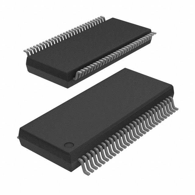
IDTCV115F is a 56 pin clock device, complying the latest Intel CK410E
requirements, for Intel advance P4 processors. The CPU output buffer is
designed to support up to 400MHz processor. One dedicated PLL for Serial
ATA clock provides high accuracy frequency. This device also implements
Band-gap referenced IREF to reduce the impact of VDD variation on differential
outputs, which can provide more robust system performance.
Each CPU/SRC/PCI, SATA clock has its own Spread Spectrum selection,
which allows for isolated changes instead of affecting other clock groups.
One high precision N and SSC programmable PLL for SRC/PCI
One high precision N and SSC programmable PLL for CPU
One high precision SSC programmable PLL for SATA
One high precision PLL for 96MHz/48MHz
Band-gap circuit for differential outputs
Support multiple spread spectrum modulation, down and
center
• Support SMBus block read/write, index read/write
• Selectable output strength for REF, PCI, and USB48MHz
• Available in SSOP package
KEY SPECIFICATIONS:
• CPU/SRC CLK cycle to cycle jitter < 85ps
• SATA CLK cycle to cycle jitter < 85ps
FUNCTIONAL BLOCK DIAGRAM
SATA PLL
SCC
Programmable
SRC4 - SATA
SATA/
PCI[4:0], PCIF[2:0]
PCI/
PCIEX PLL
SCC
N Programmable
14.318MHz
Osc
PCIE/
SRC[6:5] [3:1]
CPU2_ITP/
SRC7
MUX
CPU PLL
SCC
N Programmable
Host/
CPU[1:0]
USB48
48MHz/
Fixed PLL
No SCC
DOT96
96MHz/
REF
OUTPUT TABLE
CPU
CPU2_ITP/SRC
SRC
SATA
PCI/PCIF
REF
DOT96
48MHz
2
1
5
1
8
1
1
1
The IDT logo is a registered trademark of Integrated Device Technology, Inc.
COMMERCIAL TEMPERATURE RANGE
APRIL 2005
1
© 2005 Integrated Device Technology, Inc.
DSC - 6758/8
�IDTCV115F
PROGRAMMABLE FLEXPC™ CLOCK FOR P4 PROCESSOR
COMMERCIAL TEMPERATURE RANGE
PIN CONFIGURATION
ABSOLUTE MAXIMUM RATINGS(1)
Symbol
VDD_PCI
1
56
PCI1
VSS_PCI
2
55
PCI0
Description
Min
VDDA
3.3V Core Supply Voltage
VDD
3.3V Logic Input Supply Voltage GND - 0.5
TSTG
Storage Temperature
–65
PCI2
3
54
FS_A
PCI3
4
53
VDD_suspend
TAMBIENT
Ambient Operating Temperature
REF0
TCASE
Case Temperature
ESD Prot
Input ESD Protection
PCI4
5
52
VSS_PCI
6
51
VSS_REF
VDD_PCI
7
50
XTAL_IN
PCIF0/ITP_EN
8
49
XTAL_OUT
PCIF1
9
48
VDD_REF
SCL
PCIF2
10
47
VDD_48
11
46
SDA
USB48MHz
12
45
CPUT0
0
44
CPUC0
14
43
VDD_CPU
DOT_96#
15
42
CPUT1
VTT_PWRGD#/PWRDWN
16
TEST MODE SELECT(1)
41
CPUC1
If TEST_SEL sampled above 2V at VTT_PWRGD active LOW
SRCT1
17
40
VSS_CPU
SRCC1
18
39
IREF
VDD_SRC
19
38
FS_B/Test_Mode
VSS_SRC
20
37
FS_C/Test _Sel
SRCT2
21
36
CPU2_ITP/SRCT7
SRCC2
22
35
CPU2_ITP/SRCC7
34
VDD_SRC
24
33
SRCT6
VSS_SATA
25
32
SRCC6
SRCT4_SATA
26
31
SRCT5
SRCC4_SATA
27
30
SRCC5
VDD_SATA
28
29
VSS_SRC
4.6
V
+150
°C
+70
°C
+115
°C
V
NOTE:
1. Stresses greater than those listed under ABSOLUTE MAXIMUM RATINGS may cause
permanent damage to the device. This is a stress rating only and functional operation
of the device at these or any other conditions above those indicated in the operational
sections of this specification is not implied. Exposure to absolute maximum rating
conditions for extended periods may affect reliability.
13
23
V
Human Body Model
VSS_48
SRCT3
Unit
4.6
2000
DOT_96
SRCC3
Max
Pin38
(test_mode)
1
0
CPU
REF/N
Hi-Z
SRC
REF/N
Hi-Z
PCI/F
REF/N
Hi-Z
REF
REF
Hi-Z
DOT96
REF/N
Hi-Z
USB
REF/N
Hi-Z
NOTE:
1. Once test clock operation has been invoked, TEST_MODE pin will select between
the Hi-Z and REF/N.
ITP_EN
ITP_EN
1
0
SSOP
TOP VIEW
pin 38
CPUC2_ITP
SRCC7
pin 39
CPUT_ITP
SRCT7
HW FREQUENCY SELECTION TABLE
FSC, B, A
CPU
SRC4_SATA
SRC[3:1], SCR[7:5]
PCI
USB
DOT
REF
101
100
100
100
33.3
48
96
14.318
001
133
100
100
33.3
48
96
14.318
011
166
100
100
33.3
48
96
14.318
010
200
100
100
33.3
48
96
14.318
000
266
100
100
33.3
48
96
14.318
100
333
100
100
33.3
48
96
14.318
110
400
100
100
33.3
48
96
14.318
111
Reserve
100
100
33.3
48
96
14.318
2
�IDTCV115F
PROGRAMMABLE FLEXPC™ CLOCK FOR P4 PROCESSOR
COMMERCIAL TEMPERATURE RANGE
PIN DESCRIPTION
Pin Number
1
2
3
4
5
6
7
8
9
10
11
12
13
14
15
16
Name
VDD _PCI
VSS_PCI
PCI2
PCI3
PCI4
VSS_PCI
VDD _PCI
PCIF0/ITP_EN
PCIF1
PCIF2
VDD_48
USB48
VSS_48
DOT_96T
DOT_96C
VTT_PWRGD#/PWRDWN
Type
PWR
GND
OUT
OUT
OUT
GND
PWR
I/O
OUT
OUT
PWR
OUT
GND
OUT
OUT
IN
17
18
19
20
21
22
23
24
25
26
27
28
29
30
31
32
33
34
35
36
37
38
39
40
41
42
43
44
45
46
SRCT1
SRCC1
VDD_SRC
VSS
SRCT2
SRCC2
SRCT3
SRCC3
VSS
SRCT4_SATA
SRCC4_SATA
VDD_SRC
VSS_SRC
SRCC5
SRCT5
SRCC6
SRCT6
VDD_SRC
CPUC2_ITP/ SRCC7
CPUT2_ITP/ SRCT7
FS_C/Test_Sel
FS_B/ Test_Mode
IREF
VSS
CPUC1
CPUT1
VDD_CPU
CPUC0
CPUT0
SDA
OUT
OUT
PWR
GND
OUT
OUT
OUT
OUT
GND
OUT
OUT
PWR
GND
OUT
OUT
OUT
OUT
PWR
OUT
OUT
IN
IN
OUT
GND
OUT
OUT
PWR
OUT
OUT
I/O
Description
3.3V
GND
PCI clock
PCI clock
PCI clock
GND
3.3V
PCI clock, free running. CPU_2 select (sampled at VTT_PWRGD# assertion), HIGH = CPU_2.
PCI clock, free running
PCI clock, free running
3.3V
48MHz clock
GND
96MHz 0.7V current mode differential clock output
96MHz 0.7V current mode differential clock output
3.3V LVTTL input is a level-sensitive strobe used to latch the FS_A, FS_B, FS_C/TEST_SEL and
PCIF_0/ITP_EN inputs. After VTT_PWRGD# assertion, becomes a real-time input for asserting power
down (active high). Internal pull LOW.
Differential Serial reference clock
Differential Serial reference clock
3.3V
GND
Differential Serial reference clock
Differential Serial reference clock
Differential Serial reference clock
Differential Serial reference clock
GND
SATA clock
SATA clock
3.3V
GND
Differential Serial reference clock
Differential Serial reference clock
Differential Serial reference clock
Differential Serial reference clock
3.3V
Selectable CPU or SRC differential clock output. ITP_EN=0 @ VTT_PWRGD# assertion = SRC_7
Selectable CPU or SRC differential clock output. ITP_EN=0 @ VTT_PWRGD# assertion = SRC_7
CPU frequency selection. Selects test mode if pulled above 2V when VTT_PWRGD# is asserted.
CPU frequency selection. In test mode, 1=Hi-Z, 0=REF/N.
Reference current for differential output buffer
GND
Host 0.7V current mode differential clock output
Host 0.7V current mode differential clock output
3.3V
Host 0.7V current mode differential clock output
Host 0.7V current mode differential clock output
SMBus data
3
�IDTCV115F
PROGRAMMABLE FLEXPC™ CLOCK FOR P4 PROCESSOR
COMMERCIAL TEMPERATURE RANGE
PIN DESCRIPTION (CONT.)
Pin Number
Name
Type
47
48
49
50
51
52
53
SCL
VDD_REF
XTAL_OUT
XTAL_IN
VSS_REF
REF0
VDD_Suspend
IN
PWR
OUT
IN
GND
OUT
PWR
54
55
56
FS_A
PCI0
PCI1
IN
OUT
OUT
Description
SMBus CLK
3.3V
Xtal output
Xtal input
GND
14.318 MHz reference clock output
In the power down mode, supply 3.3V to SM control registers,
很抱歉,暂时无法提供与“IDTCV115FPVG8”相匹配的价格&库存,您可以联系我们找货
免费人工找货