IDTCV122C
PROGRAMMABLE FLEXPC™ CLOCK FOR P4 PROCESSOR
COMMERCIAL TEMPERATURE RANGE
IDTCV122C
PROGRAMMABLE FLEXPC™
CLOCK FOR P4 PROCESSOR
FEATURES:
DESCRIPTION:
•
•
•
•
•
•
IDTCV122C is a 56 pin clock device, complying the latest Intel CK410
requirements, for Intel advance P4 processors. The CPU output buffer is
designed to support up to 400MHz processor. One dedicated PLL for Serial
ATA clock provides high accuracy frequency. This device also implements
Band-gap referenced IREF to reduce the impact of VDD variation on differential
outputs, which can provide more robust system performance.
Each CPU/SRC/PCI, SATA clock has its own Spread Spectrum selection,
which allows for isolated changes instead of affecting other clock groups.
One high precision N Programming PLL for CPU
One high precision N Programming PLL for SRC/PCI
One high precision PLL for SATA
One high precision PLL for 96MHz/48MHz
Band-gap circuit for differential outputs
Support multiple spread spectrum modulation, down and
center
• Support I2C block read/write, index read/write
• Selectable output strength for REF, PCI, and 48MHz
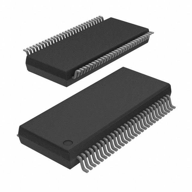
• Available in SSOP package
Not recommended for new designs.
The last time buy for this product is 12/17/2010.
Please refer to PDN K-10-15.
KEY SPECIFICATION:
• CPU/SRC CLK cycle to cycle jitter < 85ps
• SATA CLK cycle to cycle jitter < 85ps
• Static PLL frequency divide error = 0 ppm
FUNCTIONAL BLOCK DIAGRAM
SATA PLL
SCC
SRC4 - SATA
SATA/
PCI[5:0], PCIF[2:0]
PCI/
PCIEX PLL
SCC
N Programming
14.318MHz
Osc
PCIE/
SRC[6:5] [3:1]
MUX
CPU PLL
SCC
N Programming
Host/
CPU_ITP/
SRC7
CPU[1:0]
USB48
48MHz/
24_48MHz
DOT96
Fixed PLL
No SCC
96MHz/
REF[1:0]
RESET
OUTPUT TABLE
CPU
CPU_ITP/SRC
SRC
SATA
PCI/PCIF
REF/PCI
REF
DOT96
24_48MHz
RESET
TURBO
2
1
5
1
8
1
1
1
2
1
1
The IDT logo is a registered trademark of Integrated Device Technology, Inc.
COMMERCIAL TEMPERATURE RANGE
JULY 2010
1
© 2010 Integrated Device Technology, Inc.
DSC - 6590/5
�IDTCV122C
PROGRAMMABLE FLEXPC™ CLOCK FOR P4 PROCESSOR
COMMERCIAL TEMPERATURE RANGE
PIN CONFIGURATION
VDD_PCI
1
56
PCI1
VSS_PCI
2
55
PCI0
PCI2
3
54
FS_A(REF1/PCI5)
PCI3
4
53
VDD_suspend
5
52
FS_C/REF0
VSS_PCI
6
51
VSS_REF
VDD_PCI
7
50
XTAL_IN
PCIF0/ITP_EN
8
49
XTAL_OUT
PCIF1
9
48
VDD_REF
PCIF2
10
47
SCL (2)
VDD_48
11
46
SDA(2)
SEL24/24_48#
12
45
CPUT0
FS_B/48MHz
VSS_48
13
44
CPUC0
14
43
VDD_CPU
DOT_96
15
42
CPUT1
DOT_96#
16
41
CPUC1
VTT_PWRGD#/PD
17
40
VSS_CPU
SRCT1
18
39
IREF
(2)
ITP_EN
1
0
(3)
PCI4/Turbo
(1)
(4)
ITP_EN
SRCC1
19
38
(RESET#)
VDD_SRC
20
37
CPU2_ITP/SRCT7
VSS
21
36
CPU2_ITP/SRCC7
SRCT2
22
35
VDD_SRC
SRCC2
23
34
SRCT6
SRCT3
24
33
SRCC6
SRCC3
25
32
SRCT5
VSS_GND
26
31
SRCC5
SRCT4_SATA
27
30
VSS_SRC
SRCC4_SATA
28
29
VDD_SRC
Pin 38
CPUC2_ITP
SRCC7
Pin 39
CPUT_ITP
SRCT7
NOTES:
1. After power on, pin 5 is tristate (see Byte 30 and Byte 2).
2. ~ 130KΩ internal pull-up.
3. After power on, REF1/PCI5 is tristate (see Byte 1).
4. ~ 130KΩ internal pull-down.
SSOP
TOP VIEW
HW FREQUENCY SELECTION TABLE
CPU Mode Selection Table
FSC, B, A
CPU
SRC4_SATA
SRC[3:1], SCR[7:5]
PCI
USB
DOT
REF
101
100
100
100
33.3
48
96
14.318
001
133
100
100
33.3
48
96
14.318
011
166
100
100
33.3
48
96
14.318
010
200
100
100
33.3
48
96
14.318
000
266
100
100
33.3
48
96
14.318
100
333
100
100
33.3
48
96
14.318
110
400
100
100
33.3
48
96
14.318
111
Reserve
100
100
33.3
48
96
14.318
2
�IDTCV122C
PROGRAMMABLE FLEXPC™ CLOCK FOR P4 PROCESSOR
COMMERCIAL TEMPERATURE RANGE
PIN DESCRIPTION
Pin Number
1
2
3
4
5
Name
VDD_PCI
VSS_PCI
PCI2
PCI3
PCI4/Turbo
Type
PWR
GND
OUT
OUT
I/O
6
7
8
9
10
11
12
VSS_PCI
VDD_PCI
PCIF0/ITP_EN
PCIF1
PCIF2
VDD_48
SEL24/24_48#
GND
PWR
I/0
OUT
OUT
PWR
I/O
13
14
15
16
17
FS_B/48MHz
VSS_48
DOT96T
DOT96C
VTT_PWRGD#/PD
I/O
GND
OUT
OUT
IN
18
19
20
21
22
23
24
25
26
27
28
29
30
31
32
33
34
35
36
37
38
39
40
41
42
43
44
45
46
SRCT1
SRCC1
VDD_SRC
VSS
SRCT2
SRCC2
SRCT3
SRCC3
VSS
SRCT4_SATA
SRCC4_SATA
VDD_SRC
VSS_SRC
SRCC5
SRCT5
SRCC6
SRCT6
VDD_SRC
CPUC2_ITP/ SRCC7
CPUT2_ITP/ SRCT7
Reset#
IREF
VSS
CPUC1
CPUT1
VDD_CPU
CPUC0
CPUT0
SDA
OUT
OUT
PWR
GND
OUT
OUT
OUT
OUT
GND
OUT
OUT
PWR
GND
OUT
OUT
OUT
OUT
PWR
OUT
OUT
OUT
OUT
GND
OUT
OUT
PWR
OUT
OUT
I/O
Description
3.3V
GND
PCI clock
PCI clock
PCI clock output or Turbo input. Byte30 bit3 mode selection. Byte30 bit3=1, PCI clock. Byte30 bit3=0,
Turbo mode. In Turbo mode, 1 = load TCN and TPN into CPU and SRC PLL.
GND
3.3V
PCI clock, free running. CPU_2 select (sampled at VTT_PWRGD# assertion), HIGH = CPU_2.
PCI clock
PCI clock
3.3V
24MHz or 48MHz mode select, SEL24=1, 24MHz, =0, 48MHz, internal pull high. 24MHz or 48MHz
clock output afterward.
CPU frequency selection. 48MHz clock afterward
GND
96MHz 0.7V current mode differential clock output
96MHz 0.7V current mode differential clock output
3.3V LVTTL input is a level-sensitive strobe used to latch the FS_A, FS_B, FS_C/TEST_SEL and
PCIF_0/ITP_EN inputs. After VTT_PWRGD assertion, becomes a real-time input for asserting power
down (active HIGH), internal pull LOW.
Differential Serial reference clock
Differential Serial reference clock
3.3V
GND
Differential Serial reference clock
Differential Serial reference clock
Differential Serial reference clock
Differential Serial reference clock
GND
SATA clock
SATA clock
3.3V
GND
Differential Serial reference clock
Differential Serial reference clock
Differential Serial reference clock
Differential Serial reference clock
3.3V
Selectable CPU or SRC differential clock output. ITP_EN=0 @ VTT_PWRGD assertion = SRCC7
Selectable CPU or SRC differential clock output. ITP_EN=0 @ VTT_PWRGD assertion = SRCT7
Reset output
Reference current for differential output buffer
GND
Host 0.7V current mode differential clock output
Host 0.7V current mode differential clock output
3.3V
Host 0.7V current mode differential clock output
Host 0.7V current mode differential clock output
SM bus data
3
�IDTCV122C
PROGRAMMABLE FLEXPC™ CLOCK FOR P4 PROCESSOR
COMMERCIAL TEMPERATURE RANGE
PIN DESCRIPTION (CONT.)
Pin Number
Name
Type
47
48
49
50
51
52
53
54
SCL
VDD_REF
XTAL_OUT
XTAL_IN
VSS_REF
FS_C/REF0
VDD_Suspend
FS_A(REF1/PCI5)
IN
PWR
OUT
IN
GND
I/O
PWR
I/O
55
56
PCI0
PCI1
OUT
OUT
Description
SM Bus CLK
3.3V
XTAL output
XTAL input
GND
CPU frequency selection input at VTT_PWRGD assertion. 14.318 reference clock output afterward.
Keep supply 3.3V in the power down
CPU frequency selection input at VTT_PWRGD assertion. 14.318 reference clock output or PCI clock,
programmed through SMBus Register Byte 1.
PCI clock
PCI clock
INDEX BLOCK WRITE PROTOCOL
Bit
1
2-9
10
11-18
19
20-27
28
29-36
37
38-45
46
# of bits
1
8
1
8
1
8
1
8
1
8
1
From
Master
Master
Slave
Master
Slave
Master
Slave
Master
Slave
Master
Slave
Master
Slave
Master
INDEX BLOCK READ PROTOCOL
Master can stop reading any time by issuing the Stop bit without waiting
until N byte (byte count bit 30-37).
Description
Start
D2h
Ack (Acknowledge)
Register offset byte (starting byte)
Ack (Acknowledge)
Byte count, N (0 is not valid)
Ack (Acknowledge)
first data byte (Offset data byte)
Ack (Acknowledge)
2nd data byte
Ack (Acknowledge)
:
Nth data byte
Acknowledge
Stop
Bit
1
2-9
10
11-18
19
20
21-28
29
30-37
38
39-46
47
48-55
# of bits
1
8
1
8
1
1
8
1
8
1
8
1
8
From
Master
Master
Slave
Master
Slave
Master
Master
Slave
Slave
Master
Slave
Master
Slave
Master
Slave
Master
Description
Start
D2h
Ack (Acknowledge)
Register offset byte (starting byte)
Ack (Acknowledge)
Repeated Start
D3h
Ack (Acknowledge)
Byte count, N (Byte 8)
Ack (Acknowledge)
first data byte (Offset data byte)
Ack (Acknowledge)
2nd data byte
Ack (Acknowledge)
:
Ack (Acknowledge)
Nth data byte
Not acknowledge
Stop
INDEX BYTE WRITE
INDEX BYTE READ
Setting bit[11:18] = starting address, bit[20:27] = 01h.
Setting bit[11:18] = starting address. After reading back the first data byte,
master issues Stop bit.
4
�IDTCV122C
PROGRAMMABLE FLEXPC™ CLOCK FOR P4 PROCESSOR
COMMERCIAL TEMPERATURE RANGE
CB1_[2:0], CB2_[2:0], CPU MODE
SELECTION
CB[2:0]
101
001
011
010
000
100
110
111
RESOLUTION
CPU
CPU
CPU
CPU
CPU
CPU
CPU
SRC
CPU Mode, MHz
100
133
166
200
266
333
400
RESERVE
SSC MAGNITUDE CONTROL
SMC[2:0]
000
001
010
011
100
101
110
111
N Resolution (MHz)
0.666667
0.888889
1.333333
1.333333
2.666667
2.666667
2.666667
0.666667
%
0.67%
0.67%
0.8%
0.67%
1.00%
0.8%
0.67%
0.67%
PCI
When Byte5 bit6 = 0
%
OFF
- 0.25
- 0.5
±0.125
±0.25
±0.375
±0.5
±0.75
PCIS[1:0]
00
01
10
11
S_CBS[1:0], H_CBS[1:0] BAND
SELECTION
CBS[1:0]
00
01
10
11
= 100MHz mode
= 133MHz mode
= 166MHz mode
= 200MHz mode
= 266MHz mode
= 333MHz mode
= 400MHz mode
(PCI Express)
PCI
33.33
36.36
40
S_CNS, S_PNS, H_CNS,H_PNS N
SELECTION
NS[1:0]
00
01
10
11
FS[C,B,A]
CB1_[2:0]
CB2_[2:0]
Don’t care
Standard of Each CPU Mode (Band)
N Selection 1
N Selection 2
Don’t care
S.E. CLOCK STRENGTH SELECTION (PCI, REF, USB48)
Str[1:0]
00
01
10
11
2L
1H
1L
2H
Multiple loads
Recommend
Single loads
USB48
Recommend
Recommend
Recommend
Recommend
Recommend
5
N=
150
150
125
150
100
125
150
150
�IDTCV122C
PROGRAMMABLE FLEXPC™ CLOCK FOR P4 PROCESSOR
COMMERCIAL TEMPERATURE RANGE
BYTE 0
Bit
Output(s) Affected
Description/Function
0
1
Type
Power On
7
CPUT2, CPUC2/
SRCT7, SRCC7
SRCT6, SRCC6
SRCT5, SRCC5
SRCT4, SRCC4 (SATA)
SRCT3, SRCC3
SRCT2, SRCC2
SRCT1, SRCC1
REF0 2x drive
Output Enable
Tristate
Enable
RW
1
Output Enable
Output Enable
Output Enable
Output Enable
Output Enable
Output Enable
2x Drive Enable
Tristate
Tristate
Tristate
Tristate
Tristate
Tristate
1x
Enable
Enable
Enable
Enable
Enable
Enable
2x
RW
RW
RW
RW
RW
RW
RW
1
1
1
1
1
1
1
Bit
Output(s) Affected
Description/Function
0
1
Type
Power On
7
6
5
4
3
2
1
0
DOT96T, DOT96C
24_48
USB48
REF1/PCI5
REF0
CPUT1, CPUC1
CPUT0, CPUC0
REF1/PCI5
Output Enable
Output Enable
Output Enable
Mode Select
Output Enable
Output Enable
Output Enable
Output Enable
Tristate
Tristate
Tristate
PCI5
Tristate
Tristate
Tristate
Tristate
Enable
Enable
Enable
REF1
Enable
Enable
Enable
Enable
RW
RW
RW
RW
RW
RW
RW
RW
1
1
1
0
1
1
1
0
Bit
Output(s) Affected
Description/Function
0
1
Type
Power On
7
6
5
4
3
2
1
0
PCI4
PCI3
PCI2
PCI1
PCI0
PCIF2
PCIF1
PCIF0
Output Enable
Output Enable
Output Enable
Output Enable
Output Enable
Output Enable
Output Enable
Output Enable
Tristate
Tristate
Tristate
Tristate
Tristate
Tristate
Tristate
Tristate
Enable
Enable
Enable
Enable
Enable
Enable
Enable
Enable
RW
RW
RW
RW
RW
RW
RW
RW
1
1
1
1
1
1
1
1
6
5
4
3
2
1
0
BYTE 1
BYTE 2
BYTE 3
Bit
7
6
5
4
3
2
1
0
Output(s) Affected
Description / Function
SRCT[7:1]
CPUT2
CPUT1
CPUT0
DOT96T
FSC latched value on power up
FSB latched value on power up
FSA latched value on power up
SRCT Pwrdwn drive mode
CPUT2 Pwrdwn drive mode
CPUT1 Pwrdwn drive mode
CPUT0 Pwrdwn drive mode
DOT96 power down drive mode
0
Driven in power down
Driven in power down
Driven in power down
Driven in power down
Driven in power down
6
1
Type
Power On
Tristate in power down
Tristate in power down
Tristate in power down
Tristate in power down
Tristate
R
R
R
RW
RW
RW
RW
RW
0
0
0
0
0
�IDTCV122C
PROGRAMMABLE FLEXPC™ CLOCK FOR P4 PROCESSOR
COMMERCIAL TEMPERATURE RANGE
BYTE 4
Bit
Output(s) Affected
Description / Function
7
6
5
4
3
2
1
0
PCIFStr1
PCIFStr0
PCIStrC1
PCIStrC0
REFStr1
REFStr0
48MHStr1
48MHzStr0
PCIF strength selection
0
1
Type
Power On
0
0
0
1
0
0
1
1
PCI strength selection
REF strength selection
USB48MHz0 strength selection
BYTE 5
Bit
Output(s) Affected
Description / Function
0
1
Type
Power On
7
6
5
PCIPLLS
PCIS1
PCI PLL select
See PCIS table, only valid when
Byte5 bit 6 = 0 See PCIS Table
SATA PLL
PCI EX PLL
RW
RW
0
0
During the Power Down
Reset SM to default
SM contents have
no change
RW
RW
0
1
RW
RW
RW
0
1
0
Type
Power On
4
3
PCIS0
SM control registers
contents
SATA_SMC2
SATA_SMC1
SATA_SMC0
SATA PLL spread spectrum
magnitude control select
(see SMC table)
Bit
Output(s) Affected
Description / Function
7
WDHRB
6
WDSRB
5
4
3
2
1
0
SRC_SMC2
SRC_SMC1
SRC_SMC0
CPU_SMC2
CPU_SMC1
CPU_SMC0
Hard Alarm read back,
reset by WD disable
Soft Alarm read back,
rest by WD disable
SRC(PCIEXpress)
PLL spread spectrum magnitude
control select (see SMC table)
CPU PLL spread spectrum
control magnitude select
(see SMC table)
Output(s) Affected
Description / Function
2
1
0
BYTE 6
0
1
R
R
RW
RW
RW
RW
RW
RW
0
1
0
1
0
0
Type
Power On
BYTE 7
Bit
7
6
5
4
3
2
1
0
0
Revision ID
Revision ID
Revision ID
Revision ID
Vendor ID
Vendor ID
Vendor ID
Vendor ID
1
0
0
0
0
0
1
0
1
7
�IDTCV122C
PROGRAMMABLE FLEXPC™ CLOCK FOR P4 PROCESSOR
COMMERCIAL TEMPERATURE RANGE
BYTE 8
Bit
Output(s) Affected
Description / Function
0
1
7
6
5
4
3
2
1
0
Type
Power On
RW
RW
RW
RW
RW
RW
RW
RW
0
0
0
1
1
1
1
1
Type
Power On
RW
RW
RW
RW
RW
RW
RW
RW
0
0
0
Type
Power On
RW
RW
RW
RW
RW
RW
RW
RW
1
0
0
1
0
1
1
0
Type
Power On
BYTES 9 - 16 ARE DUMMY BITES
BYTE 17
Bit
Output(s) Affected
Description / Function
7
6
5
4
3
2
1
0
CB1_2
CB1_1
CB1_0
CPU PLL Band Selection 1
(see CPU Mode Selection table)
CB2_2
CB2_1
CB2_0
CN1_8 (MSB)
CPU PLL Band Selection 2
(see CPU Mode Selection table)
Bit
Output(s) Affected
Description / Function
7
6
5
4
3
2
1
0
CN1_7
CN1_6
CN1_5
CN1_4
CN1_3
CN1_2
CN1_1
CN1_0 (LSB)
0
1
CPU PLL N selection 1
0
0
0
0
BYTE 18
0
1
CPU PLL N selection 1
CPU Frequency = N * Resolution
(see Resolution table)
BYTE 19
Bit
Output(s) Affected
7
6
5
4
3
2
1
0
CN2_8 (MSB)
CN2_7
CN2_6
CN2_5
CN2_4
CN2_3
CN2_2
CN2_1
Description / Function
0
1
0
1
0
0
1
0
1
1
CPU N selection 2
CPU Frequency = N * Resolution
(see Resolution table)
8
�IDTCV122C
PROGRAMMABLE FLEXPC™ CLOCK FOR P4 PROCESSOR
COMMERCIAL TEMPERATURE RANGE
BYTE 20
Bit
Output(s) Affected
Description / Function
7
6
5
4
3
2
1
0
CN2_0 (LSB)
CPU N selection 2
0
1
Type
Power On
0
PN1_8 (MSB)
PN1_7
RW
RW
0
1
Type
Power On
RW
RW
RW
RW
RW
RW
RW
RW
0
0
1
0
1
1
0
0
Type
Power On
RW
RW
RW
RW
RW
RW
RW
RW
1
0
0
1
0
1
1
0
Type
Power On
RW
0
RW
RW
RW
RW
0
0
0
0
RW
0
BYTE 21
Bit
Output(s) Affected
7
6
5
4
3
2
1
0
PN1_6
PN1_5
PN1_4
PN1_3
PN1_2
PN1_1
PN1_0 (LSB)
PN2_8 (MSB)
Description / Function
SRC PLL (PCI Express)
N Selection 1
SRC Frequency = N * Resolution
Resolution = 0.666667
Bit
Output(s) Affected
Description / Function
7
6
5
4
3
2
1
0
PN2_7
PN2_6
PN2_5
PN2_4
PN2_3
PN2_2
PN2_1
PN2_0 (LSB)
0
1
BYTE 22
0
1
SRC PLL (PCI Express)
N Selection 1
SRC Frequency = N * Resolution
Resolution = 0.666667
BYTE 23
Bit
Output(s) Affected
Description / Function
7
S_CBS1
6
5
4
3
S_CBS0
S_CNS1
S_CNS0
S_PNS1
2
1
0
S_PNS0
Soft Alarm CPU PLL mode
select (see S_CBS Band
Selection Table)
Soft Alarm CPU PLL N select
(see S_CNS N Selection Table)
Soft Alarm SRC PLL (PCI
Express) N select
(see S_PNS N Selection Table)
0
9
1
�IDTCV122C
PROGRAMMABLE FLEXPC™ CLOCK FOR P4 PROCESSOR
COMMERCIAL TEMPERATURE RANGE
BYTE 24
Bit
Output(s) Affected
Description / Function
7
6
5
4
3
H_CBS1
H_CBS0
H_CNS2
H_CNS0
H_PNS1
2
1
0
H_PNS0
Hard Alarm CPU PLL mode select
(see H_CBS Band Selection table)
Hard Alarm CPU PLL N select
(see H_CNS N Selection table)
Hard Alarm SRC PLL
(PCI Express) N select
(see H_PNS N selection table)
0
1
Type
Power On
RW
RW
RW
RW
RW
0
0
0
0
0
RW
0
Type
Power On
RW
RW
RW
RW
RW
RW
RW
RW
0
0
0
0
1
0
1
1
Type
Power On
RW
RW
RW
RW
RW
RW
RW
RW
0
0
0
1
BYTE 25
Bit
Output(s) Affected
Description / Function
7
6
5
4
3
2
1
0
WD Timer 7 (MSB)
WD Timer 6
WD Timer 5
WD Timer 4
WD Timer 3
WD Timer 2
WD Timer 1
WD Timer 0 (LSB)
Hard Alarm timer
Default is 11*290ms
Output(s) Affected
Description / Function
0
1
BYTE 26
Bit
7
6
5
4
3
2
1
0
0
1
Soft Timer 3 (MSB)
Soft Timer 2
Soft Timer 1
Soft Timer 0 (LSB)
Soft alarm timer
Bit
Output(s) Affected
Description / Function
0
1
Type
Power On
7
6
5
4
3
2
1
Watch Dog Enable
Watch Dog Enable
Disable
Enable
RW
0
Soft Alarm Enable
Soft RESET#
Hard Alarm Enable
Hard RESET#
Hard Alarm FS
Relatch Enable
TCN8 (MSB)
Soft Alarm Enable
Soft Reset Enable
Hard Alarm Enable
Hard Reset Enable
Relatch FS[C, B, A]
at Hard Alarm
Disable
Disable
Disable
Disable
Disable
Enable
Soft Reset Enable
Enable
Hard Reset Enable
Relatch
RW
RW
RW
RW
RW
0
0
0
0
0
RW
0
BYTE 27
0
10
�IDTCV122C
PROGRAMMABLE FLEXPC™ CLOCK FOR P4 PROCESSOR
COMMERCIAL TEMPERATURE RANGE
BYTE 28
Bit
Output(s) Affected
7
6
5
4
3
2
1
0
TCN7
TCN6
TCN5
TCN4
TCN3
TCN2
TCN1
TCN0 (LSB)
Description / Function
0
1
Turbo CPU PLL N setting
CPU Frequency = N * Resolution
(see Resolution table)
Type
Power On
RW
RW
RW
RW
RW
RW
RW
RW
1
0
0
1
0
1
1
0
Type
Power On
BYTE 29
Bit
Output(s) Affected
7
6
5
4
3
2
1
0
TPN8 (MSB)
TPN7
TPN6
TPN5
TPN4
TPN3
TPN2
TPN1
Description / Function
0
1
0
1
0
0
1
0
1
1
Turbo SRC PLL N setting
SRC Frequency = N * Resolution
Resolution = 0.666667
BYTE 30
Bit
Output(s) Affected
7
6
5
TPN0 (LSB)
4
3
2
1
PCI4/Turbo
Turbo
Test_scl
0
Test_hiz
Description / Function
0
1
Type
Power On
0
Test Mode entry control
Normal operation
Only valid when Byte6 bit5 is high
PCI4/Turbo Mode select
On chip test mode enable
Hi-Z
Turbo
Disable
normal
CLK outputs enable
normal
11
Test mode,
controlled by byte 30 bit 4
REF/N mode
PCI4
Enable
SCLK=1, CLK outputs=1
SCLK=0, CLK outputs=0
CLK outputs=Tristate
0
RW
RW
RW
0
0
0
0
RW
0
�IDTCV122C
PROGRAMMABLE FLEXPC™ CLOCK FOR P4 PROCESSOR
COMMERCIAL TEMPERATURE RANGE
PLL FREQUENCY PROGRAMMING PROCEDURES
The user changes PLL frequency through Soft Alarm or Hard Alarm. The Watch Dog circuit has to be enabled. Based on their application, the user may
enable either one or both of the alarms.
User presets the CPU PLL Mode and N, and SRC PLL N value:
1. Set CPU PLL Mode, CB1 and CB2, byte17
2. Set CPU PLL N, CN1 and CN2, byte18 and byte19
3. Set SRC(PCI Express) PLL N, PN1 and PN2, byte21, 22
User selects the frequency for Soft Alarm and Hard Alarm, if enabled respectively:
4. Select Soft Alarm frequency, byte23
5. Select Hard Alarm frequency, byte24
User sets the Timer and enables the WD circuit for frequency switch:
6. Set Hard Alarm Timer, byte25
7. Set Soft Alarm Timer, byte 26
8. Enable Soft and Hard Alarm and RESET# bit (If user needs RESET# signal to reset the system), byte27
9. Enable Watch Dog (WDE), byte27
•
•
•
Soft Reset# and Hard Reset# are valid only if Soft Alarm and Hard Alarm are enabled respectively.
WDE Disable resets WDSRB and WDHRB.
PCI CLK is selectable from SRC PLL or SATA PLL, byte5 bit6. If from SRC PLL, PCI frequency = 1/3 of SRC frequency. If from SATA, PCI is
fixed to 3 selections, 33MHz, 36MHz and 40MHz, byte5 bit[5:4].
WD SOFT AND HARD ALARM/TIME OUT OPERATION
WD HARD ALARM TIMER [7:0]
WD SOFT ALARM TIMER [3:0]
WDE
Trigger Watch Dog Circuit
If Soft Alarm Enabled (byte 27):
Set WDSRB (byte 6)
Load CPU N and Mode
selections into PCU PLL
Load SRC N selection
into SRC PLL
If Soft Reset# Enabled (byte 27):
Issue RESET#
12
If Hard Alarm Enabled (byte 27):
Set WDHRB (byte 6)
Load CPU N and Band selections into PCU PLL
Load SRC N selections into SRC PLL
If Hard Reset# Enabled (byte 27):
Issue RESET#
If Hard Alarm Relatch Enabled:
Latch FSC, B, A
�IDTCV122C
PROGRAMMABLE FLEXPC™ CLOCK FOR P4 PROCESSOR
COMMERCIAL TEMPERATURE RANGE
ELECTRICAL CHARACTERISTICS - INPUT / SUPPLY / COMMON OUTPUT
PARAMETERS
Following Conditions Apply Unless Otherwise Specified:
Operating Condition: TA = 0°C to +70°C, Supply Voltage: VDD = 3.3V ± 5%
Symbol
Parameter
Test Conditions
Min.
Typ.
Max.
Unit
VIH
Input HIGH Voltage
3.3V ± 5%
2
—
VDD + 0.3
V
VIL
Input LOW Voltage
3.3V ± 5%
VSS - 0.3
—
0.8
V
VIH_FS
FS Input HIGH Voltage
For FSA.B.C and Test_Mode
0.7
—
VDD + 0.3
V
VIL_FS
FS Input LOW Voltage
For FSA.B.C and Test_Mode
VSS - 0.3
—
0.35
V
IIH
Input HIGH Current
VIN = VDD
–5
—
5
µA
IIL1
Input LOW Current
VIN = 0V, inputs with no pull-up resistors
–5
—
—
µA
IIL2
Input LOW Current
VIN = 0V, inputs with pull-up resistors
–200
—
—
µA
IDD3.3OP
Operating Supply Current
Full active, CL = full load
—
—
400
mA
IDD3.3PD
Powerdown Current
All differential pairs driven
—
—
70
mA
All differential pairs tri-stated
—
—
12
VDD = 3.3V
—
14.31818
—
MHz
—
—
7
nH
Logic inputs
—
—
5
Output pin capacitance
—
—
6
FI
Input Frequency(1)
LPIN
Pin Inductance(2)
CIN
COUT
Input Capacitance(2)
CINX
TSTAB
pF
XTAL_IN and XTAL_OUT
—
—
6
Clock Stabilization(2,3)
From VDD power-up or de-assertion of PD# to first clock
—
—
1.8
ms
Modulation Frequency(2)
Triangular modulation
30
—
33
KHz
TDRIVE_SRC(2)
SRC output enable after PCI_Stop# de-assertion
—
—
15
ns
TDRIVE_PD#(2)
CPU output enable after PD# de-assertion
—
—
300
us
TFALL_PD#(2)
Fall time of PD#
—
—
5
ns
TRISE_PD#(2)
Rise time of PD#
—
—
5
ns
TDRIVE_CPU_Stop#(2)
CPU output enable after CPU_Stop# de-assertion
—
—
10
us
TFALL_CPU_Stop#(2)
Fall time of PD#
—
—
5
ns
TRISE_CPU_Stop#(2)
Rise time of PD#
—
—
5
ns
NOTES:
1. Input frequency should be measured at the REF output pin and tuned to ideal 14.31818MHz to meet ppm frequency accuracy on PLL outputs.
2. This parameter is guaranteed by design, but not 100% production tested.
3. See TIMING DIAGRAMS for timing requirements.
13
�IDTCV122C
PROGRAMMABLE FLEXPC™ CLOCK FOR P4 PROCESSOR
COMMERCIAL TEMPERATURE RANGE
ELECTRICAL CHARACTERISTICS - CPU, SRC, AND DOT96 0.7 CURRENT MODE
DIFFERENTIAL PAIR(1)
Following Conditions Apply Unless Otherwise Specified:
Operating Condition: TA = 0°C to +70°C, Supply Voltage: VDD = 3.3V ± 5%; CL = 2pF
Symbol
Parameter
Min.
Typ.
Max.
Unit
VO = VX
3000
—
—
Ω
Output HIGH Voltage
IOH = -1mA
2.4
—
—
V
VOL3
Output LOW Voltage
IOL = 1mA
—
—
0.4
V
VHIGH
Voltage HIGH(2)
Statistical measurement on single-ended signal using
660
—
1150
mV
VLOW
Voltage LOW(2)
oscilloscope math function
–300
—
150
VOVS
Max Voltage(2)
Measurement on single-ended signal using absolute value
—
—
1150
VUDS
Min Voltage(2)
–300
—
—
VCROSS(ABS)
Crossing Voltage (abs)(2)
250
—
550
mV
d - VCROSS
Crossing Voltage (var)(2)
Variation of crossing over all edges
—
—
140
mV
Long Accuracy(2,3)
See TPERIOD Min. - Max. values
–300
—
300
ppm
Current Source Output Impedance(2)
VOH3
ZO
ppm
TPERIOD
TABSMIN
Average Period(3)
Absolute Min Period(2,3)
Test Conditions
400MHz nominal / -0.5% spread
2.4993
—
2.5133
333.33MHz nominal / -0.5% spread
2.9991
—
3.016
266.66MHz nominal / -0.5% spread
3.7489
—
3.77
200MHz nominal / -0.5% spread
4.9985
—
5.0266
166.66MHz nominal / -0.5% spread
5.9982
—
6.032
133.33MHz nominal / -0.5% spread
7.4978
—
7.54
100MHz nominal / -0.5% spread
9.997
—
10.0533
96MHz nominal
10.4135
—
10.4198
400MHz nominal / -0.5% spread
2.4143
—
—
333.33MHz nominal / -0.5% spread
2.9141
—
—
266.66MHz nominal / -0.5% spread
3.6639
—
—
200MHz nominal / -0.5% spread
166.66MHz nominal / -0.5% spread
4.9135
5.9132
—
—
—
—
133.33MHz nominal / -0.5% spread
7.4128
—
—
100MHz nominal / -0.5% spread
9.912
—
—
10.1635
—
—
96MHz nominal
mV
ns
ns
tR
Rise Time(2)
VOL = 0.175V, VOH = 0.525V
175
—
700
ps
tF
Fall Time(2)
VOL = 0.175V, VOH = 0.525V
175
—
700
ps
—
—
125
ps
—
45
—
—
125
55
ps
%
d-tR
Rise Time Variation(2)
d-tF
dT3
Fall Time Variation(2)
Duty Cycle(2)
Measurement from differential waveform
NOTES:
1. SRC clock outputs run only at 100MHz.
2. This parameter is guaranteed by design, but not 100% production tested.
3. All long term accuracy and clock period specifications are guaranteed with the assumption that the REF output is at 14.31818MHz.
14
�IDTCV122C
PROGRAMMABLE FLEXPC™ CLOCK FOR P4 PROCESSOR
COMMERCIAL TEMPERATURE RANGE
ELECTRICAL CHARACTERISTICS - CPU, SRC, AND DOT96 0.7 CURRENT MODE
DIFFERENTIAL PAIR, CONTINUED(1)
Following Conditions Apply Unless Otherwise Specified:
Operating Condition: TA = 0°C to +70°C, Supply Voltage: VDD = 3.3V ± 5%; CL = 2pF
Symbol
tSK3
tJCYC-CYC
Parameter
Skew, CPU[1:0](2)
Skew, CPU2(2)
Min.
—
—
Typ.
—
—
Max.
100
250
Skew, SRC(2)
—
—
250
Jitter, Cycle to Cycle, CPU[1:0](2)
—
—
85
—
—
100
—
—
—
—
125
250
Jitter, Cycle to Cycle, CPU2(2)
Test Conditions
VT = 50%
Measurement from differential waveform
Jitter, Cycle to Cycle, SRC(2)
Jitter, Cycle to Cycle, DOT96(2)
Unit
ps
ps
NOTES:
1. SRC clock outputs run only at 100MHz.
2. This parameter is guaranteed by design, but not 100% production tested.
ELECTRICAL CHARACTERISTICS - PCICLK / PCICLK_F
Following Conditions Apply Unless Otherwise Specified:
Operating Condition: TA = 0°C to +70°C, Supply Voltage: VDD = 3.3V ± 5%; CL = 10 - 30pF
Symbol
Parameter
Test Conditions
ppm
Static Error(1,2)
Min.
Typ.
Max.
Unit
See Tperiod Min. - Max. values
TPERIOD
Clock Period(2)
—
—
0
ppm
33.33MHz output nominal
29.991
—
30.009
ns
33.33MHz output spread
29.991
—
30.1598
VOH
Output HIGH Voltage
IOH = -1mA
2.4
—
—
V
VOL
Output LOW Voltage
IOL = 1mA
—
—
0.55
V
IOH
Output HIGH Current
VOH at Min. = 1V
-33
—
—
mA
VOH at Max. = 3.135V
—
—
-33
VOL at Min. = 1.95V
30
—
—
IOL
Output LOW Current
mA
VOL at Max. = 0.4V
—
—
38
Edge Rate(1)
Rising edge rate
1
—
4
V/ns
Edge Rate(1)
Falling edge rate
1
—
4
V/ns
tR1
Rise Time(1)
VOL = 0.8V, VOH = 2V
0.3
—
1.2
ns
tF1
Fall Time(1)
VOL = 0.8V, VOH = 2V
0.3
—
1.2
ns
VT = 1.5V
45
—
55
%
VT = 1.5V
—
—
500
ps
VT = 1.5V
—
—
500
ps
Cycle(1)
dT1
Duty
tSK1
Skew(1)
tJCYC-CYC
Jitter, Cycle to
Cycle(1)
NOTES:
1. This parameter is guaranteed by design, but not 100% production tested.
2. All long term accuracy and clock period specifications are guaranteed with the assumption that the REF output is at 14.31818MHz.
15
�IDTCV122C
PROGRAMMABLE FLEXPC™ CLOCK FOR P4 PROCESSOR
COMMERCIAL TEMPERATURE RANGE
ELECTRICAL CHARACTERISTICS, 48MHZ, USB
Following Conditions Apply Unless Otherwise Specified:
Operating Condition: TA = 0°C to +70°C, Supply Voltage: VDD = 3.3V ± 5%; CL = 10 - 20pF
Symbol
Parameter
Test Conditions
ppm
Static Error(1,2)
See Tperiod Min. - Max. values
TPERIOD
Clock Period(2)
48MHz output nominal
VOH
Output HIGH Voltage
VOL
IOH
IOL
Min.
Typ.
Max.
Unit
—
—
0
ppm
20.8257
—
20.834
ns
IOH = -1mA
2.4
—
—
V
Output LOW Voltage
IOL = 1mA
—
—
0.55
V
Output HIGH Current
VOH at Min. = 1V
-29
—
—
mA
VOH at Max. = 3.135V
—
—
-23
VOL at Min. = 1.95V
29
—
—
Output LOW Current
mA
VOL at Max. = 0.4V
—
—
27
Edge Rate(1)
Rising edge rate
1
—
2
V/ns
Edge Rate(1)
Falling edge rate
1
—
2
V/ns
tR1
Rise Time(1)
VOL = 0.8V, VOH = 2V
0.5
—
1.2
ns
tF1
Fall Time(1)
VOL = 0.8V, VOH = 2V
0.5
—
1.2
ns
dT1
Duty Cycle(1)
VT = 1.5V
45
—
55
%
—
—
350
ps
Min.
Typ.
Max.
Unit
—
—
0
ppm
69.827
—
69.855
ns
tJCYC-CYC
Jitter, Cycle to Cycle
NOTES:
1. This parameter is guaranteed by design, but not 100% production tested.
2. All long term accuracy and clock period specifications are guaranteed with the assumption that the REF output is at 14.31818MHz.
ELECTRICAL CHARACTERISTICS - REF-14.318MHZ
Following Conditions Apply Unless Otherwise Specified:
Operating Condition: TA = 0°C to +70°C, Supply Voltage: VDD = 3.3V ± 5%; CL = 10 - 20pF
Symbol
Parameter
Test Conditions
Long Accuracy(1)
See Tperiod Min. - Max. values
Clock Period
14.318MHz output nominal
VOH
Output HIGH Voltage(1)
IOH = -1mA
2.4
—
—
V
VOL
Output LOW Voltage(1)
IOL = 1mA
—
—
0.4
V
IOH
Output HIGH Current
VOH at Min. = 1V
-33
—
—
mA
VOH at Max. = 3.135V
—
—
-33
VOL at Min. = 1.95V
30
—
—
ppm
TPERIOD
IOL
Output LOW Current
mA
VOL at Max. = 0.4V
—
—
38
Edge Rate(1)
Rising edge rate
1
—
4
V/ns
Edge Rate(1)
Falling edge rate
1
—
4
V/ns
tR1
Rise Time(1)
VOL = 0.8V, VOH = 2V
0.3
—
1.2
ns
tF1
Fall Time(1)
VOL = 0.8V, VOH = 2V
0.3
—
1.2
ns
VT = 1.5V
45
—
55
%
VT = 1.5V
—
—
1000
ps
dT1
tJCYC-CYC
Duty
Cycle(1)
Jitter, Cycle to Cycle(1)
NOTE:
1. This parameter is guaranteed by design, but not 100% production tested.
16
�IDTCV122C
PROGRAMMABLE FLEXPC™ CLOCK FOR P4 PROCESSOR
COMMERCIAL TEMPERATURE RANGE
PD, POWER DOWN
PD is an asynchronous active low input used to shut off all clocks cleanly prior to clock power. When PD is asserted low all clocks will be driven low before
turning off the VCO. In PD de-assertion all clocks will start without glitches.
PWRDWN
CPU
CPU#
SRC
SRC#
PCIF/PCI
USB
0
Normal
1
IREF * 2 or float
DOT96
DOT96#
REF
Normal
Normal
Normal
33MHz
Float
IREF * 2 or float
Float
Low
48MHz
Normal
Normal
14.318MHz
Low
IREF * 2 or float
Float
Low
PD ASSERTION
PD should be sampled low by two consecutive CPU# rising edges before stopping clocks. All single-ended clocks will be held low on their next high to low
transition. All differential clocks will be held high on the next high to low transition of the complimentary clock. If the control register determining to drive mode
is set to ‘tri-state’, the differential pair will be stopped in tri-state mode, undriven. When the drive mode but corresponding to the CPU or SRC clock of interest
is set to ‘0’ the true clock will be driven high at 2 x IREF and the complementary clock will be tristated. If the control register is programmed to ‘1’ both clocks will
be tristated.
PWRDWN
CPU 133MHz
CPU# 133MHz
SRC 100MHz
SRC# 100MHz
USB 48MHz
PCI 33MHz
REF 14.31818
17
�IDTCV122C
PROGRAMMABLE FLEXPC™ CLOCK FOR P4 PROCESSOR
COMMERCIAL TEMPERATURE RANGE
PD DE-ASSERTION
The time from the de-assertion of PD or until power supply ramps to get stable clocks will be less than 1.8ms. If the drive mode control bit for PD tristate is
programmed to ‘1’ the stopped differential pair must first be driven high to a minimum of 200mV in less than 300µs of PD deassertion.
tSTABLE


 工商网监
湘ICP备2023018690号
工商网监
湘ICP备2023018690号
