IDTCV149
PROGRAMMABLE FLEXPC™ CLOCK FOR AMD K8 PROCESSOR ATI RS480
COMMERCIAL TEMPERATURE RANGE
IDTCV149
PROGRAMMABLE FLEXPC™
CLOCK FOR AMD K8
PROCESSOR ATI RS480
FEATURES:
DESCRIPTION:
• One high precision N and SSC programmable PLL for CPU
• One high precision N and SSC programmable PLL for SRC[2:1]
• One high precision N and SSC programmable PLL for SRC0
[7:3] (PCI Express)
• One high precision PLL for 48MHz
• Band-gap circuit for differential outputs
• Support multiple spread spectrum modulation, down and
center
• Support SMBus block read/write, index read/write
• Selectable output strength for REF, PCI, 48MHz, HTT66
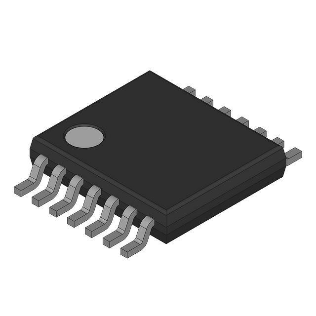
• Available in SSOP and TSSOP packages
IDTCV149 is a 56 pin clock device for AMD advance K8 processors. The
CPU output buffer is designed to support up to 400MHz processor. This device
also implements Band-gap referenced IREF to reduce the impact of VDD variation
on differential outputs, which can provide more robust system performance.
Each CPU/SRC clock has its own Spread Spectrum selection, which allows
for isolated changes instead of affecting other clock groups.
KEY SPECIFICATION:
• CPU CLK cycle to cycle jitter < 85ps
• SRC CLK cycle to cycle jitter < 100ps
• Static PLL frequency divide error = 0 ppm
FUNCTIONAL BLOCK DIAGRAM
SRC
SSC
N Programming
SRC[7:3], 0
SRC
PCI0
PCI/
SRC PLL
SSC
N Programming
14.318MHz
Osc
SRC/
CLKREQ0#
CLKREQ1#
CPU PLL
SSC
N Programming
Host/
Fixed PLL
No SSC
48MHz/
SRC[2:1]
CPU[1:0]
HTT66
TURBO1#
USB48
24_48MHz
REF[2:0]
Reset#
OUTPUT TABLE
CPU
CLKREQ
SRC
HTT66
PCI
TURBO
USB48
24_48
REF
RESET#
2
2
8
1
1
1
1
1
3
1
The IDT logo is a registered trademark of Integrated Device Technology, Inc.
COMMERCIAL TEMPERATURE RANGE
MAY 2004
1
© 2004 Integrated Device Technology, Inc.
DSC - 6497/2
�IDTCV149
PROGRAMMABLE FLEXPC™ CLOCK FOR AMD K8 PROCESSOR ATI RS480
CPU AND SRC SPREAD SPECTRUM
MAGNITUDE CONTROL
PIN CONFIGURATION
(1)
(1)
XIN
1
56
VDD_REF
XOUT
2
55
VSS_REF
VDD_48
3
54
REF0
USB_48
4
53
REF1
VSS_48
5
52
REF2
CLK_STOP
6
51
VDD_PC1
SCL
7
50
PCI0
SDA
8
49
VSS_PCI
SEL24/24_48#
CLKREQ0#
9
48
VDD_HTT
10
47
HTT66
CLKREQ1#
11
46
VSS_HTT
SRCT7
12
45
CPUT0
SRCC7
13
44
CPUC0
VDD_SRC
14
43
VDD_CPU
RESET#
15
42
VSS_CPU
SRCT6
16
41
CPUT1
SRCC6
17
40
CPUC1
SRCT5
18
39
VDDA
SRCC5
19
38
VSSA
VSS_SRC
20
37
IREF
VDD_SRC
21
36
VSS_SRC
SRCT4
22
35
VDD_SRC
SRCC4
23
34
SRCT0
SRCT3
24
33
SRCC0
SRCC3
25
32
VDD_SRC
TURBO1
26
31
VSS_SRC
SRCT2
27
30
SRCT1
SRCC2
28
29
SRCC1
(2)
(2)
COMMERCIAL TEMPERATURE RANGE
SMC[2:0]
000
001
010
011
100
101
110
111
%
OFF
- 0.25
- 0.5
- 0.75
±0.125
±0.25
±0.375
±0.5
SE SIGNAL STRENGTH SELECTION
Str[1:0]
00
01
10
11
Strength
0.6x
0.8x
1x
1.2x
PCI (BASED ON SRC = 100MHz)
PCIS[1:0]
00
01
10
11
NOTES:
1. Internal 130KΩ pull-down resistor.
2. Tristate at power on to be compatible with ATI pin definition.
SSOP/ TSSOP
TOP VIEW
2
PCI
33.33
36.36
40
30.77
�IDTCV149
PROGRAMMABLE FLEXPC™ CLOCK FOR AMD K8 PROCESSOR ATI RS480
COMMERCIAL TEMPERATURE RANGE
PIN DESCRIPTION
Pin Name
XIN
XOUT
PCI0
HTT66
USB48
Turbo1
CPUC[1:0]
CPUT[1:0]
SRCC[7:0]
SRCT[7:0]
Type
IN
OUT
OUT
OUT
OUT
IN
OUT
Pin #
1
2
50
47
4
26
40, 41, 44, 45
OUT
IREF
REF[1:0]
REF2
CLKREQ0#
CLKREQ1#
SDA
SCL
SEL24/24_48#
CLK_STOP
RESET#
OUT
OUT
OUT
IN
IN
I/O
IN
IN
IN
OUT,
OD
12, 13, 16, 17, 18, 19,
22, 23, 24, 25, 27, 28,
29, 30, 33, 34
37
53, 54
52
10
11
8
7
9
6
15
Description
XTAL in
XTAL out
PCI clock
66.66 MHz
48MHz
Turbo frequency select
Differential clock
Differential clock
Differential clock reference current
14.318MHz
14.318MHz
SRC OE control, see bytes 3, 4
SRC OE control, see bytes 3, 4
SMBus data
SMBus clock
Latched select input for 24 or 48MHz output. 1 = 24MHz, 0 = 48MHz.
Active HIGH, drives all clocks to LOW (except CPU clocks)
Reset output signal, Open Drain
3
�IDTCV149
PROGRAMMABLE FLEXPC™ CLOCK FOR AMD K8 PROCESSOR ATI RS480
COMMERCIAL TEMPERATURE RANGE
SM PROTOCOL
INDEX BLOCK WRITE PROTOCOL
Bit
1
2-9
10
11-18
19
20-27
28
29-36
37
38-45
46
# of bits
1
8
1
8
1
8
1
8
1
8
1
From
Master
Master
Slave
Master
Slave
Master
Slave
Master
Slave
Master
Slave
Master
Slave
Master
INDEX BLOCK READ PROTOCOL
Master can stop reading any time by issuing the stop bit without waiting
until Nth byte (byte count bit30-37).
Description
Start
D2h
Ack (Acknowledge)
Register offset byte (starting byte)
Ack (Acknowledge)
Byte count, N (0 is not valid)
Ack (Acknowledge)
first data byte (Offset data byte)
Ack (Acknowledge)
2nd data byte
Ack (Acknowledge)
:
Nth data byte
Acknowledge
Stop
Bit
1
2-9
10
11-18
19
20
21-28
29
30-37
# of bits
1
8
1
8
1
1
8
1
8
From
Master
Master
Slave
Master
Slave
Master
Master
Slave
Slave
38
39-46
47
48-55
1
8
1
8
Master
Slave
Master
Slave
Master
Slave
Master
INDEX BYTE READ
INDEX BYTE WRITE
Description
Start
D2h
Ack (Acknowledge)
Register offset byte (starting byte)
Ack (Acknowledge)
Repeated Start
D3h
Ack (Acknowledge)
Byte count, N (block read back of N
bytes), power on is 8
Ack (Acknowledge)
first data byte (Offset data byte)
Ack (Acknowledge)
2nd data byte
Ack (Acknowledge)
:
Ack (Acknowledge)
Nth data byte
Not acknowledge
Stop
Setting bit[11:18] = starting address. After reading back the first data byte,
master issues Stop bit.
Setting bit[11:18] = starting address, bit[20:27] = 01h.
4
�IDTCV149
PROGRAMMABLE FLEXPC™ CLOCK FOR AMD K8 PROCESSOR ATI RS480
COMMERCIAL TEMPERATURE RANGE
BYTE 0
Bit
Output(s) Affected
Description/Function
0
1
Type
Power On
7
6
5
4
3
2
1
0
SRCT7, SRCC7
SRCT6, SRCC6
SRCT5, SRCC5
SRCT4, SRCC4
SRCT3, SRCC3
SRCT2, SRCC2
SRCT1, SRCC1
SRCT0, SRCT0
Output enable
Output enable
Output enable
Output enable
Output enable
Output enable
Output enable
Output enable
Tristate
Tristate
Tristate
Tristate
Tristate
Tristate
Tristate
Tristate
Enable
Enable
Enable
Enable
Enable
Enable
Enable
Enable
RW
RW
RW
RW
RW
RW
RW
RW
1
1
1
1
1
1
1
1
Bit
Output(s) Affected
Description/Function
0
1
Type
Power On
7
6
5
4
3
2
1
0
USB48
REF2
REF1
REF0
24_48MHz
CPUT1, CPUC1
CPUT0, CPUC0
HTT66
Output enable
Output enable
Output enable
Output enable
Output enable
Output enable
Output enable
Output enable
Tristate
Tristate
Tristate
Tristate
Tristate
Tristate
Tristate
Tristate
Enable
Enable
Enable
Enable
Enable
Enable
Enable
Enable
RW
RW
RW
RW
RW
RW
RW
RW
1
1
1
1
1
1
1
1
BYTE 1
BYTE 2
Bit
Output(s) Affected
Description / Function
0
1
Type
Power On
7
6
5
4
3
2
1
0
PCI0
Reserved
PCI0 SEL1
PCI0 SEL0
Reserved
SRCs
CPUT1
CPUT0
Output enable
Tristate
Enable
SRCT PWRDWN drive mode
CPUT1 PWRDWN drive mode
CPUT0 PWRDWN drive mode
Driven in power down
Driven in power down
Driven in power down
Tristate in power down
Tristate in power down
Tristate in power down
RW
RW
RW
RW
RW
RW
RW
RW
1
0
0
0
0
0
0
0
Bit
Output(s) Affected
Description / Function
7
6
5
4
3
2
1
0
SRC7
SRC6
SRC5
SRC4
SRC3
Reserved
Reserved
SRC0
see PCI select table
BYTE 3
Controlled by CLKREQB#
or CLKREQA#
Controlled by CLKREQB#
or CLKREQA#
5
0
1
Type
Power On
CLKREQ0#
CLKREQ0#
CLKREQ0#
CLKREQ0#
CLKREQ0#
CLKREQ1#
CLKREQ1#
CLKREQ1#
CLKREQ1#
CLKREQ1#
CLKREQ0#
CLKREQ1#
RW
RW
RW
RW
RW
RW
RW
RW
0
0
0
0
0
0
0
0
�IDTCV149
PROGRAMMABLE FLEXPC™ CLOCK FOR AMD K8 PROCESSOR ATI RS480
COMMERCIAL TEMPERATURE RANGE
BYTE 4
Bit
Output(s) Affected
7
6
5
4
3
2
1
0
SRC7
SRC6
SRC5
SRC4
SRC3
Reserved
Reserved
SRC0
Description / Function
When CLKREQ is HIGH,
Output is Hi-Z
When CLKREQ is HIGH,
Output is Hi-Z
0
1
Type
Power On
Not Controlled
Not Controlled
Not Controlled
Not Controlled
Not Controlled
Controlled
Controlled
Controlled
Controlled
Controlled
Not Controlled
Controlled
RW
RW
RW
RW
RW
RW
RW
RW
0
0
0
0
0
0
0
0
BYTE 5
Bit
Output(s) Affected
Description / Function
7
6
5
4
3
2
1
0
HTT66
HTT66
PCIStrC1
PCIStrC0
REFStr1
REFStr0
48MHStr1
48MHzStr0
HTT66 strength selection
0
1
PCI strength selection
REF strength selection
USB48MHz strength selection
Type
Power On
RW
RW
RW
RW
RW
RW
RW
RW
1
0
1
0
1
0
1
0
BYTE 6
Bit
Output(s) Affected
7
6
5
4
3
2
1
0
Reserve
SRC0, SR[7:3], SMC2
SRC0, SR[7:3], SMC1
SRC0, SR[7:3], SMC0
Reserved
SRC[2:1], SMC2
SRC[2:1], SMC1
SRC[2:1], SMC0
Description / Function
0
1
SRC0, SRC[7:3] SSC control
(see SMC table)
SRC[2:1] control (see SMC table)
Type
Power On
RW
RW
RW
RW
RW
RW
RW
RW
0
0
0
0
0
0
0
0
Type
Power On
R
R
R
R
R
R
R
R
0
0
0
0
0
1
0
1
BYTE 7
Bit
7
6
5
4
3
2
1
0
Output(s) Affected
Description / Function
0
Revision ID
Revision ID
Revision ID
Revision ID
Vendor ID
Vendor ID
Vendor ID
Vendor ID
6
1
�IDTCV149
PROGRAMMABLE FLEXPC™ CLOCK FOR AMD K8 PROCESSOR ATI RS480
COMMERCIAL TEMPERATURE RANGE
BYTE 8 (INDEX BLOCK READ BYTE COUNT)
Bit
Output(s) Affected
Description / Function
0
1
7
6
5
4
3
2
1
0
Type
Power On
RW
RW
RW
RW
RW
RW
RW
RW
0
0
0
1
0
1
1
0
Type
Power On
RW
RW
RW
RW
RW
RW
RW
RW
0
0
0
0
0
0
0
0
Type
Power On
RW
RW
RW
RW
RW
RW
RW
RW
0
0
0
0
1
0
1
1
BYTE 9
Bit
Output(s) Affected
7
6
5
4
3
2
1
0
Reserved
Reserved
Reserved
Reserved
Reserved
CPU SMC2
CPU SMC1
CPU SMC0
Description / Function
0
1
CPU PLL SSC control
(see SMC table)
BYTE 10
Bit
Output(s) Affected
7
6
5
4
3
2
1
0
WD_1_ Timer 7
WD_1_ Timer 6
WD_1_ Timer 5
WD_1_ Timer 4
WD_1_ Timer 3
WD_1_ Timer 2
WD_1_ Timer 1
WD_1_ Timer 0
Description / Function
0
1
WatchDog_1_Alarm timer
Default is 11*290ms
BYTE 11
Bit
Output(s) Affected
7
6
5
4
3
CPU_N8
Reserved
Reserved
Reserved
WDRB
2
1
0
RESET#(1)
Reserved
Watch Dog Enable
Description / Function
0
1
Type
Power On
Alarm
RW
RW
RW
RW
R
0
0
0
0
0
RW
RW
RW
0
0
0
Alarm read back,
reset by WD disable
Reset Enable
Disable
Reset Enable
Watch Dog Enable
Disable
Enable
7
�IDTCV149
PROGRAMMABLE FLEXPC™ CLOCK FOR AMD K8 PROCESSOR ATI RS480
COMMERCIAL TEMPERATURE RANGE
BYTE 12
Bit
Output(s) Affected
7
6
5
4
3
2
1
0
CPU_N7
CPU_N6
CPU_N5
CPU_N4
CPU_N3
CPU_N2
CPU_N1
CPU_N0, LSB
Description / Function
CPU CLK = N*Resolution
Resolution = 1.3333
Bit
Output(s) Affected
Description / Function
7
6
5
4
3
2
1
0
SRC1_N7, MSB
SRC1_N6
SRC1_N5
SRC1_N4
SRC1_N3
SRC1_N2
SRC1_N1
SRC1_N0, LSB
0
1
Type
Power On
RW
RW
RW
RW
RW
RW
RW
RW
1
0
0
1
0
1
1
0
Type
Power On
RW
RW
RW
RW
RW
RW
RW
RW
1
0
0
1
0
1
1
0
Type
Power On
RW
RW
RW
RW
RW
RW
RW
RW
1
0
0
1
0
1
1
0
BYTE 13
0
1
SRC2, SRC1
SRC CLK = N*Resolution
Resolution = 0.66667
BYTE 14
Bit
Output(s) Affected
7
6
5
4
3
2
1
0
SRC0_N7, MSB
SRC0_N6
SRC0_N5
SRC0_N4
SRC0_N3
SRC0_N2
SRC0_N1
SRC0_N0, LSB
Description / Function
0
1
SRC[7:3], SRC0
SRC CLK = N*Resolution
Resolution = 0.66667
BYTE 15
Bit
Output(s) Affected
7
6
5
4
3
2
1
0
CPU N programming enable
SRC1, SRC2 N Programming enable
SRC0, SRC[7:3] N Programming enable
Turbo1 enable
Turbo
Reserved
T1CN8
Description / Function
0
1
Type
Power On
Turbo Active Selection
Disable
Disable
Disable
Disable
Disable
Active HIGH
Enable
Enable
Enable
Enable
Enable
Active LOW
RW
RW
RW
RW
RW
RW
RW
RW
0
0
0
0
0
0
0
0
8
�IDTCV149
PROGRAMMABLE FLEXPC™ CLOCK FOR AMD K8 PROCESSOR ATI RS480
COMMERCIAL TEMPERATURE RANGE
BYTE 16
Bit
Output(s) Affected
7
6
5
4
3
2
1
0
T1CN7
T1CN6
T1CN5
T1CN4
T1CN3
T1CN2
T1CN1
T1CN0
Description / Function
0
1
Turbo1 CPU PLL N setting
CLK = N*Resolution
Resolution = 1.3333
Type
Power On
RW
RW
RW
RW
RW
RW
RW
RW
1
0
0
1
0
1
1
0
Type
Power On
RW
RW
RW
RW
RW
RW
RW
RW
1
0
0
1
0
1
1
0
Type
Power On
RW
RW
RW
RW
RW
RW
RW
RW
0
0
0
0
0
0
0
0
Type
Power On
RW
RW
RW
RW
RW
RW
RW
RW
0
0
0
0
0
0
0
0
BYTE 17
Bit
Output(s) Affected
7
6
5
4
3
2
1
0
TSRC1_N7, MSB
TSRC1_N6
TSRC1_N5
TSRC1_N4
TSRC1_N3
TSRC1_N2
TSRC1_N1
TSRC1_N0, LSB
Description / Function
0
1
Turbo1
SRC2, SRC1
SRC CLK = N*Resolution
Resolution = 0.66667
BYTE 18 (RESERVED FOR USER)
Bit
Output(s) Affected
Description / Function
0
1
7
6
5
4
3
2
1
0
BYTE 19 (RESERVED FOR USER)
Bit
Output(s) Affected
Description / Function
0
7
6
5
4
3
2
1
0
9
1
�IDTCV149
PROGRAMMABLE FLEXPC™ CLOCK FOR AMD K8 PROCESSOR ATI RS480
COMMERCIAL TEMPERATURE RANGE
BYTE 20 (RESERVED FOR USER)
Bit
Output(s) Affected
Description / Function
0
1
7
6
5
4
3
2
1
0
Type
Power On
RW
RW
RW
RW
RW
RW
RW
RW
0
0
0
0
0
0
0
0
Type
Power On
RW
RW
RW
RW
RW
RW
RW
0
0
0
0
0
0
0
RW
0
BYTE 21
Bit
Output(s) Affected
Description / Function
0
7
6
5
4
3
2
1
Reserved
Reserved
Reserved
Reserved
Reserved
Reserved
Test_scl
On chip test mode enable
Normal
0
Test_hiz
CLK outputs enable
Normal
BYTE 62 = 70h
BYTE 63 = 13h
ABSOLUTE MAXIMUM RATINGS(1)
Symbol
Description
Min
Max
Unit
VDDA
3.3V Core Supply Voltage
4.6
V
VDD
3.3V I/O Supply Voltage
4.6
V
VIH
3.3V Input HIGH
4.6
V
VID
3.3V Input LOW
–0.5
TS
Storage Temperature
–65
ESD Prot
Input ESD Protection
2000
V
+150
°C
V
Human Body Model
NOTE:
1. Stresses greater than those listed under ABSOLUTE MAXIMUM RATINGS may cause
permanent damage to the device. This is a stress rating only and functional operation
of the device at these or any other conditions above those indicated in the operational
sections of this specification is not implied. Exposure to absolute maximum rating
conditions for extended periods may affect reliability.
10
1
SCLK = 1, CLK outputs = 1
SCLK = 0, CLK outputs = 0
CLK outputs = Tristate
�IDTCV149
PROGRAMMABLE FLEXPC™ CLOCK FOR AMD K8 PROCESSOR ATI RS480
COMMERCIAL TEMPERATURE RANGE
ELECTRICAL CHARACTERISTICS - INPUT / SUPPLY / COMMON OUTPUT
PARAMETERS
Following Conditions Apply Unless Otherwise Specified:
Operating Condition: TA = 0°C to +70°C, Supply Voltage: VDD = 3.3V ± 5%
Symbol
Parameter
Test Conditions
Min.
Typ.
Max.
Unit
VIH
Input HIGH Voltage
3.3V ± 5%
2
—
VDD + 0.3
V
VIL
Input LOW Voltage
3.3V ± 5%
VSS - 0.3
—
0.8
V
VIH_FS
3.3V Input HIGH Voltage
VDD
0.7
—
VDD + 0.3
V
VIL_FS
3.3V Input LOW Voltage
VSS - 0.3
—
0.35
V
IIH
Input HIGH Current
VIN = VDD
–5
—
5
µA
IIL1
Input LOW Current
VIN = 0V, inputs with no pull-up resistors
–5
—
—
µA
IIL2
Input LOW Current
VIN = 0V, inputs with pull-up resistors
–200
—
—
µA
Operating Supply Current
Full active, CL = full load
—
—
400
mA
FI
Input Frequency(1)
VDD = 3.3V
—
14.31818
—
MHz
LPIN
Pin Inductance(2)
—
—
7
nH
IDD3.3OP
CIN
COUT
Input Capacitance(2)
CINX
TSTAB
Logic inputs
—
—
5
Output pin capacitance
—
—
6
pF
X1 and X2 pins
—
—
5
Clock Stabilization(2,3)
From VDD power-up
—
—
1.8
ms
Modulation Frequency(2)
Triangular modulation
30
—
33
KHz
NOTES:
1. Input frequency should be measured at the REF output pin and tuned to ideal 14.31818MHz to meet ppm frequency accuracy on PLL outputs.
2. This parameter is guaranteed by design, but not 100% production tested.
3. See TIMING DIAGRAMS for timing requirements.
11
�IDTCV149
PROGRAMMABLE FLEXPC™ CLOCK FOR AMD K8 PROCESSOR ATI RS480
COMMERCIAL TEMPERATURE RANGE
ELECTRICAL CHARACTERISTICS - SRC 0.7 CURRENT MODE DIFFERENTIAL PAIR
Following Conditions Apply Unless Otherwise Specified:
Operating Condition: TA = 0°C to +70°C, Supply Voltage: VDD = 3.3V ± 5%; CL = 2pF
Symbol
Parameter
Min.
Typ.
Max.
Unit
VO = VX
3000
—
—
Ω
Output HIGH Voltage
IOH = -1mA
2.4
—
—
V
VOL3
Output LOW Voltage
IOL = 1mA
—
—
0.4
V
VHIGH
Voltage HIGH(1)
Statistical measurement on single-ended signal using
660
—
1150
mV
VLOW
Voltage LOW(1)
oscilloscope math function
–300
—
150
VOVS
Max Voltage(1)
Measurement on single-ended signal using absolute value
—
—
1150
VUDS
Min Voltage(1)
–300
—
—
VCROSS(ABS)
Crossing Voltage (abs)(1)
250
—
550
mV
d - VCROSS
Crossing Voltage (var)(1)
Variation of crossing over all edges
—
—
140
mV
ppm
Long Accuracy(1,2)
See TPERIOD Min. - Max. values
–300
—
300
ppm
TPERIOD
Average Period(2)
100MHz nominal
9.997
—
10.003
ns
TABSMIN
Absolute Min Period(1,2)
100MHz nominal
9.912
—
—
ns
tR
Rise Time(1)
VOL = 0.175V, VOH = 0.525V
175
—
700
ps
tF
Fall Time(1)
VOL = 0.175V, VOH = 0.525V
175
—
700
ps
Current Source Output Impedance(1)
VOH3
ZO
Test Conditions
mV
d-tR
Rise Time Variation(1)
—
—
125
ps
d-tF
Fall Time Variation(1)
—
—
125
ps
dT3
Cycle(1)
Measurement from differential waveform
45
—
55
%
Measurement from differential waveform
—
—
125
ps
tJCYC-CYC
SKEW
Duty
Jitter, Cycle to
Cycle(1)
Pin-to-Pin Skew(1)
VT = 50%
—
—
250
ps
TSU_SRC(1,3)
SRC STOP response to CLKREQ#
—
—
60
ns
TDRIVE_SRC(1,3)
SRC START response to CLKREQ#
—
—
60
ns
NOTES:
1. This parameter is guaranteed by design, but not 100% production tested.
2. All long term accuracy and clock period specifications are guaranteed with the assumption that the REF output is at 14.31818MHz.
3. See TIMING DIAGRAMS for timing requirements.
12
�IDTCV149
PROGRAMMABLE FLEXPC™ CLOCK FOR AMD K8 PROCESSOR ATI RS480
COMMERCIAL TEMPERATURE RANGE
ELECTRICAL CHARACTERISTICS - CPU DIFFERENTIAL PAIR (SSC ENABLE AND
DISABLE)
Following Conditions Apply Unless Otherwise Specified:
Operating Condition: TA = 0°C to +70°C, Supply Voltage: VDD = 3.3V ± 5%; CL = 2pF
Symbol
Parameter(1)
Test Conditions
Min.
Typ.
Max.
Unit
tR
Rise Edge Rate
2
—
10
V/ns
tF
Fall Edge Rate
2
—
10
V/ns
VDIFF
Differential Voltage (single end)
0.4
1.25
2.3
V
∆VDIFF
Change in VDIFF_DC Magnitude
–150
—
+150
mV
VCM
Common Mode Voltage
1.05
1.25
1.45
V
∆VCM
Change in Common Mode Voltage
–200
—
+200
mV
—
—
200
ps
–1000
—
—
—
+1000
3
ps
ms
tCCJITTER
Jitter, Cycle to Cycle
tJA
tFS
Jitter Accumulated
Frequency Stabilization from
Power-Up
RON
Output Impedance
15
35
55
Ω
Duty Cycle
47
50
53
%
–300
—
+300
ppm
ns
Duty Cycle
ppm
Long Accuracy(2)
See TPERIOD Min. - Max. values
TPERIOD
Average Period(2)
200MHz nominal
4.9985
—
5.0015
250MHz nominal
3.9988
—
4.0012
NOTES:
1. Parameters guaranteed by design, but not 100% production tested.
2. All long term accuracy and clock period specifications are guaranteed with the assumption that the REF output is at 14.31818MHz.
13
�IDTCV149
PROGRAMMABLE FLEXPC™ CLOCK FOR AMD K8 PROCESSOR ATI RS480
COMMERCIAL TEMPERATURE RANGE
ELECTRICAL CHARACTERISTICS - PCICLK / PCICLK_F, HTT66
Following Conditions Apply Unless Otherwise Specified:
Operating Condition: TA = 0°C to +70°C, Supply Voltage: VDD = 3.3V ± 5%; CL = 10 - 30pF
Symbol
ppm
TPERIOD
Parameter
Test Conditions
Min.
Typ.
Max.
Unit
Long Accuracy(1,2)
See Tperiod Min. - Max. values
—
—
300
ppm
Clock Period(2)
33.33MHz output nominal
29.991
—
30.009
ns
33.33MHz output spread
29.991
—
30.1598
VOH
Output HIGH Voltage
IOH = -1mA
2.4
—
—
V
VOL
Output LOW Voltage
IOL = 1mA
—
—
0.55
V
IOH
Output HIGH Current
VOH at Min. = 1V
-33
—
—
mA
VOH at Max. = 3.135V
—
—
-33
VOL at Min. = 1.95V
30
—
—
IOL
Output LOW Current
mA
VOL at Max. = 0.4V
—
—
38
Edge Rate(1)
Rising edge rate
1
—
4
V/ns
Edge Rate(1)
Falling edge rate
1
—
4
V/ns
tR1
Rise Time(1)
VOL = 0.8V, VOH = 2V
0.3
—
1.2
ns
tF1
Fall Time(1)
VOL = 0.8V, VOH = 2V
0.3
—
1.2
ns
dT1
Duty Cycle(1)
VT = 1.5V
45
—
55
%
VT = 1.5V
—
—
500
ps
Min.
Typ.
Max.
Unit
—
—
300
ppm
20.8257
—
20.834
ns
tJCYC-CYC
Jitter, Cycle to
Cycle(1)
NOTES:
1. This parameter is guaranteed by design, but not 100% production tested.
2. All long term accuracy and clock period specifications are guaranteed with the assumption that the REF output is at 14.31818MHz.
ELECTRICAL CHARACTERISTICS - 24_48MHZ, 48MHZ, USB
Following Conditions Apply Unless Otherwise Specified:
Operating Condition: TA = 0°C to +70°C, Supply Voltage: VDD = 3.3V ± 5%; CL = 10 - 20pF
Symbol
Parameter
Test Conditions
Long Accuracy(1,2)
See Tperiod Min. - Max. values
Clock Period(2)
48MHz output nominal
VOH
Output HIGH Voltage
IOH = -1mA
2.4
—
—
V
VOL
Output LOW Voltage
IOL = 1mA
—
—
0.55
V
IOH
Output HIGH Current
VOH at Min. = 1V
-29
—
—
mA
VOH at Max. = 3.135V
—
—
-23
VOL at Min. = 1.95V
29
—
—
ppm
TPERIOD
IOL
Output LOW Current
mA
VOL at Max. = 0.4V
—
—
27
Edge Rate(1)
Rising edge rate
1
—
2
V/ns
Edge Rate(1)
Falling edge rate
1
—
2
V/ns
tR1
Rise Time(1)
VOL = 0.8V, VOH = 2V
0.5
—
1.2
ns
tF1
Fall Time(1)
VOL = 0.8V, VOH = 2V
0.5
—
1.2
ns
dT1
Duty Cycle(1)
VT = 1.5V
45
—
55
%
Jitter, Cycle to Cycle(1)
VT = 1.5V
—
—
350
ps
tJCYC-CYC
NOTES:
1. This parameter is guaranteed by design, but not 100% production tested.
2. All long term accuracy and clock period specifications are guaranteed with the assumption that the REF output is at 14.31818MHz.
14
�IDTCV149
PROGRAMMABLE FLEXPC™ CLOCK FOR AMD K8 PROCESSOR ATI RS480
COMMERCIAL TEMPERATURE RANGE
ELECTRICAL CHARACTERISTICS - REF-14.318MHZ
Following Conditions Apply Unless Otherwise Specified:
Operating Condition: TA = 0°C to +70°C, Supply Voltage: VDD = 3.3V ± 5%; CL = 10 - 20pF
Symbol
Parameter
Test Conditions
Long Accuracy(1)
See Tperiod Min. - Max. values
Clock Period
14.318MHz output nominal
VOH
Output HIGH Voltage(1)
VOL
Output LOW Voltage(1)
IOH
Output HIGH Current
ppm
TPERIOD
IOL
Output LOW Current
Min.
Typ.
Max.
Unit
—
—
0
ppm
69.827
—
69.855
ns
IOH = -1mA
2.4
—
—
V
IOL = 1mA
—
—
0.4
V
VOH at Min. = 1V
-33
—
—
mA
VOH at Max. = 3.135V
—
—
-33
VOL at Min. = 1.95V
30
—
—
mA
VOL at Max. = 0.4V
—
—
38
Edge Rate(1)
Rising edge rate
1
—
4
V/ns
Edge Rate(1)
Falling edge rate
1
—
4
V/ns
tR1
Rise Time(1)
VOL = 0.8V, VOH = 2V
0.3
—
1.2
ns
tF1
Fall Time(1)
VOL = 0.8V, VOH = 2V
0.3
—
1.2
ns
VT = 1.5V
45
—
55
%
VT = 1.5V
—
—
1000
ps
dT1
tJCYC-CYC
Duty
Cycle(1)
Jitter, Cycle to
Cycle(1)
NOTE:
1. This parameter is guaranteed by design, but not 100% production tested.
15
�IDTCV149
PROGRAMMABLE FLEXPC™ CLOCK FOR AMD K8 PROCESSOR ATI RS480
COMMERCIAL TEMPERATURE RANGE
CLKREQ# ASSERTION
The clock samples the CLKREQ# signal on a rising edge of SRC clock. After detecting the CLKREQ# assertion low, all controlled SRC clocks will be tristate
on their next high to low transition.
tSU_SRC
CLKREQ#
SRC
SRC#
CLKREQ# - DE-ASSERTION
The de-assertion of the CLKREQ# signal is to be sampled on the rising edge of the SRC free running clock domain. After detecting CLKREQ# de-assertion,
all controlled SRC clocks will resume in a glitch free manner.
tDRIVE_SRC
CLKREQ#
SRC
SRC#
16
�IDTCV149
PROGRAMMABLE FLEXPC™ CLOCK FOR AMD K8 PROCESSOR ATI RS480
COMMERCIAL TEMPERATURE RANGE
ORDERING INFORMATION
IDTCV XXX
Device Type
XX
Package
X
Grade
Blank
Commercial Temperature Range
(0°C to +70°C)
PV
PA
PAG
Small Shrink Outline Package
Thin Shrink Small Outline Package
TSSOP - Green
149
Programmable FlexPC™ Clock for AMD K8
Processor ATI RS480
17
�IMPORTANT NOTICE AND DISCLAIMER
RENESAS ELECTRONICS CORPORATION AND ITS SUBSIDIARIES (“RENESAS”) PROVIDES TECHNICAL
SPECIFICATIONS AND RELIABILITY DATA (INCLUDING DATASHEETS), DESIGN RESOURCES (INCLUDING
REFERENCE DESIGNS), APPLICATION OR OTHER DESIGN ADVICE, WEB TOOLS, SAFETY INFORMATION, AND
OTHER RESOURCES “AS IS” AND WITH ALL FAULTS, AND DISCLAIMS ALL WARRANTIES, EXPRESS OR IMPLIED,
INCLUDING, WITHOUT LIMITATION, ANY IMPLIED WARRANTIES OF MERCHANTABILITY, FITNESS FOR A
PARTICULAR PURPOSE, OR NON-INFRINGEMENT OF THIRD PARTY INTELLECTUAL PROPERTY RIGHTS.
These resources are intended for developers skilled in the art designing with Renesas products. You are solely responsible
for (1) selecting the appropriate products for your application, (2) designing, validating, and testing your application, and (3)
ensuring your application meets applicable standards, and any other safety, security, or other requirements. These
resources are subject to change without notice. Renesas grants you permission to use these resources only for
development of an application that uses Renesas products. Other reproduction or use of these resources is strictly
prohibited. No license is granted to any other Renesas intellectual property or to any third party intellectual property.
Renesas disclaims responsibility for, and you will fully indemnify Renesas and its representatives against, any claims,
damages, costs, losses, or liabilities arising out of your use of these resources. Renesas' products are provided only subject
to Renesas' Terms and Conditions of Sale or other applicable terms agreed to in writing. No use of any Renesas resources
expands or otherwise alters any applicable warranties or warranty disclaimers for these products.
(Rev.1.0 Mar 2020)
Corporate Headquarters
Contact Information
TOYOSU FORESIA, 3-2-24 Toyosu,
Koto-ku, Tokyo 135-0061, Japan
www.renesas.com
For further information on a product, technology, the most
up-to-date version of a document, or your nearest sales
office, please visit:
www.renesas.com/contact/
Trademarks
Renesas and the Renesas logo are trademarks of Renesas
Electronics Corporation. All trademarks and registered
trademarks are the property of their respective owners.
© 2020 Renesas Electronics Corporation. All rights reserved.
�


 工商网监
湘ICP备2023018690号
工商网监
湘ICP备2023018690号
