DATASHEET
ISL15100
FN8577
Rev 0.00
September 19, 2013
Single Port, PLC Differential Line Driver
The ISL15100 is a single port differential line driver developed
for Power Line Communication (PLC) applications. The device
is designed to drive heavy line loads while maintaining the
high level of linearity required in OFDM PLC modem links. With
15.5dBm of total transmit signal power into 100 line load,
the driver achieves -43dB average MTPR distortion across the
output spectrum up to 86MHz.
Features
The ISL15100 has two bias current control pins (C0, C1) to
allow for four power settings (disable, low, medium, high). In
disable mode, the line driver outputs maintain a high
impedance in the presence of high receive signal amplitude,
so it doesn’t affect TDM receive signal integrity.
• -43dBc average MTPR distortion at full line power
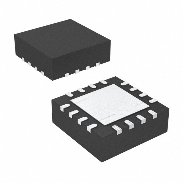
The ISL15100 is available in the thermally-enhanced 16 Ld
QFN and is specified for operation over the full -40°C to +85°C
ambient temperature range.
• Power Line Communication differential driver
• Single differential driver
• 100MHz Broadband PLC G.hn, EOC, HomePlug AV2
• Control pins for enable/disable and supply current selection
• High output impedance when disabled for TDM operation
• Single +12V or bipolar ±6V nominal supplies
• High surge current handling capability
Applications
• Pin compatible upgrade to ISL1571IRZ
Related Literature
• AN1325 “Choosing and Using Bypass Capacitors”
TABLE 1. ALTERNATE SOLUTIONS
PART #
NOMINAL ±VS
(V)
BANDWIDTH
(MHz)
APPLICATIONS
ISL1571
±6, +12
200
HomePlug AV1
+12V
100n
+
500
SUPPLY
DECOUPLING
NOT SHOW N
½ ISL15100
-30
3.9
-40
-
Vcm
Rg
133
-60
100
NOMINAL
LINE
Rf
1k
2.2n
½ ISL15100
500
100n
-50
1:2
3.9
+
POWER (dBM)
AFE
Rf
1k
-70
-80
-90
-100
-110
-120
-130
TYPICAL DIFFERENTIAL I/O LINE DRIVER
FIGURE 1. TYPICAL APPLICATION CIRCUIT
FN8577 Rev 0.00
September 19, 2013
2
7
12
17
22
27
32
37
42
47
FREQUENCY (MHz)
FIGURE 2. 50MHz PLC SPECTRUM
Page 1 of 9
�ISL15100
Connection Diagram
+12V
+
+
PLINE = 16dBm
CF = 15.4dB
Av = 1 + 2 x 1000 = 16(V/V)
133
140DIFFERENTIAL RECEIVER
PATH LOAD AT TXMN INPUT
INA+
+
OUTA
½ ISL15100
3.9
500
-
1k
1:2
INA-
500mVp +6V
133
11.8Vp
INTO PLINE
100
8.0Vp
INB-
½ ISL15100
500
INB+
Txmn
1k
OUTB
+
BIAS
CURRENT
CONTROL
3.9
C0
C1
FIGURE 3. TYPICAL DIFFERENTIAL AMPLIFIER I/O
Ordering Information
PART
NUMBER
(Notes 2, 3)
PART
MARKING
TEMP RANGE
(°C)
PACKAGE
(Pb-free)
PKG.
DWG. #
ISL15100IRZ
151 00IRZ
-40 to +85
16 Ld QFN
L16.4x4H
ISL15100IRZ-T7 (Note 1)
151 00IRZ
-40 to +85
16 Ld QFN
L16.4x4H
ISL15100IRZ-T13 (Note 1)
151 00IRZ
-40 to +85
16 Ld QFN
L16.4x4H
ISL15100EVAL1Z
Evaluation Board
NOTES:
1. Please refer to TB347 for details on reel specifications.
2. These Intersil Pb-free plastic packaged products employ special Pb-free material sets, molding compounds/die attach materials, and 100% matte
tin plate plus anneal (e3 termination finish, which is RoHS compliant and compatible with both SnPb and Pb-free soldering operations). Intersil
Pb-free products are MSL classified at Pb-free peak reflow temperatures that meet or exceed the Pb-free requirements of IPC/JEDEC J STD-020.
3. For Moisture Sensitivity Level (MSL), please see device information page for ISL15100. For more information on MSL please see tech brief TB363.
FN8577 Rev 0.00
September 19, 2013
Page 2 of 9
�ISL15100
Pin Configuration
OUTA
NC
VS+
OUTB
ISL15100
(16 LD QFN)
TOP VIEW
16
15
14
13
NC 1
12 NC
INA- 2
11 INBEP*
INA+ 3
10 INB+
5
6
7
8
NC
VS-
C0
9
NC
GND 4
C1
*EXPOSED THERMAL PAD CONNECTS TO MOST NEGATIVE SUPPLY
Pin Descriptions
PIN NUMBER
PIN NAME
EP
THERMAL PAD
1
NC
No Internal Connection
2
INA-
Amplifier A Inverting Input
3
INA+
Amplifier A Non-Inverting Input
4
GND
5
NC
No Internal Connection
6
NC
No Internal Connection
7
VS-
Negative Supply Voltage (-6V for split supplies, GND for single supply operation)
8
C0
Digital Control Pin
9
C1
Digital Control Pin
10
INB+
Amplifier B Non-Inverting Input
11
INB-
Amplifier B Inverting Input
12
NC
13
OUTB
FUNCTION
Connect to the Most Negative Supply
Ground
No Internal Connection
Amplifier B Output
14
VS+
Positive Supply Voltage (+6V for split supplies, +12V for single supply operation)
15
NC
No Internal Connection
16
OUTA
Amplifier A Output
C0, C1 Truth Table
C1
C0
0
0
High Bias Setting
0
1
Medium Bias Setting
1
0
Low Bias Setting
1
1
Outputs Disabled (Power Down)
FN8577 Rev 0.00
September 19, 2013
FUNCTION
Page 3 of 9
�ISL15100
Absolute Maximum Ratings (TA = +25°C)
Thermal Information
VS+ Voltage to VS- or GND . . . . . . . . . . . . . . . . . . . . . . . . . . . -0.3V to +13.3V
INA+, INB+ Voltage. . . . . . . . . . . . . . . . . . . . . . . . . . . . . . . . . . . . GND to VS+
C0, C1 Voltage to GND . . . . . . . . . . . . . . . . . . . . . . . . . . . . . . . . . -0.3V to VS+
Current into any Input . . . . . . . . . . . . . . . . . . . . . . . . . . . . . . . . . . . . . . . 8mA
Continuous Output Current for Long Term Reliability. . . . . . . . . . . . . . . . 50mA
Latch-up (Tested per JESD78D, Class II) . . . . . . . . . . . . . . . . . . . . . . 100mA
ESD Rating
Human Body Model (Tested per JESD22-A114F). . . . . . . . . . . . . . . . . . 4kV
Charge Device Model (Tested per JESD22-C101E). . . . . . . . . . . . . 1.5kV
Machine Model (Tested per JESD22-A115C) . . . . . . . . . . . . . . . . . 300V
Thermal Resistance (Typical)
JA (°C/W) JC (°C/W)
16 Ld QFN Package (Notes 4, 5) . . . . . . . .
53
16.5
Maximum Junction Temperature (Plastic Package) . . . . . . . . . . . +150°C
Storage Temperature Range. . . . . . . . . . . . . . . . . . . . . . . -40°C to +150°C
Pb-Free Reflow Profile . . . . . . . . . . . . . . . . . . . . . . . . . . . . . . . see link below
http://www.intersil.com/pbfree/Pb-FreeReflow.asp
Operating Conditions
Ambient Temperature Range . . . . . . . . . . . . . . . . . . . . . . . -40°C to +85°C
Junction Temperature Range . . . . . . . . . . . . . . . . . . . . . . - 40°C to +150°C
CAUTION: Do not operate at or near the maximum ratings listed for extended periods of time. Exposure to such conditions may adversely impact product
reliability and result in failures not covered by warranty.
NOTES:
4. JA is measured in free air with the component mounted on a high effective thermal conductivity test board with “direct attach” features. See Tech
Brief TB379.
5. For JC, the “case temp” location is the center of the exposed metal pad on the package underside.
Electrical Specifications
VS+ = +12V, VS- = GND = 0V, see Figure 3, Full Bias (C0 = C1 = 0V), TA = +25°C, unless otherwise specified.
PARAMETER
DESCRIPTION
CONDITIONS
MIN
(Note 6)
TYP
MAX
(Note 6)
UNIT
DYNAMIC PERFORMANCE
-3dB Bandwidth
BW
Figure 3, 2VP-P differential output at pins
180
MHz
Slew Rate
SR
Differential VOUT (VOUTA - VOUTB) from -5V
to +5V (10VP-P)
1200
V/µs
Total Harmonic Distortion
THD, Low Frequency, 200kHz, differential 12VP-P, across ≥350Ω
Light Load
differential load
-88
-67
dBc
THD, Low Frequency, 200kHz, differential 12VP-P, across 29Ω
differential load
Heavy Load
-72
-68
dBc
THD, High Frequency, 4MHz, differential 12VP-P, across ≥350Ω
Light Load
differential load
-64
-58
dBc
THD, High Frequency, 4MHz, differential 12VP-P, across 29Ω
Heavy Load
differential load
-51
-48
dBc
Avg. Multi-Tone Power Ratio
MTPR
2MHz to 50MHz, 25kHz tone spacing,
PLINE = 15.5dBm, CF = 15dB
-43
dBc
Off State Multi-Tone Power Ratio
MTPR-OFF
2MHz to 50MHz, 25kHz tone spacing,
PLINE = 15.5dBm, CF = 15dB
-55
dBc
Non-inverting Input Spot Voltage Noise
Eni
F > 1MHz, spot noise voltage on INA+ and
INB+ inputs separately
6
nV/√Hz
Non-inverting Input Spot Current Noise
Ini+
F > 1MHz, spot noise current on INA+ and
INB+ inputs separately
13
pA/√Hz
Inverting Input Spot Current Noise
Ini-
F > 1MHz, spot noise current on INA- and
INB- inputs separately
50
pA/√Hz
Non-Inverting Input Bias Current
IB+
Non-inverting inputs, INA+ and INB+, at
mid-supply voltage (Note 7)
-7
2
7
µA
Non-Inverting Input Bias Current
Mismatch
IB+DM
Difference between the INA+ and INB+
bias currents
-0.5
0
0.5
µA
Inverting Input Bias Current
IB-
Inverting inputs, INA- and INB-, at mid
supply voltage (Note 7)
-90
-30
55
µA
DC AND INPUT CHARACTERISTICS
FN8577 Rev 0.00
September 19, 2013
Page 4 of 9
�ISL15100
Electrical Specifications
VS+ = +12V, VS- = GND = 0V, see Figure 3, Full Bias (C0 = C1 = 0V), TA = +25°C, unless otherwise specified.
PARAMETER
DESCRIPTION
CONDITIONS
MIN
(Note 6)
TYP
MAX
(Note 6)
UNIT
Inverting Input Bias Current Mismatch
IB-DM
Difference between the INA- and INB- input
bias currents
-35
0
35
µA
Inverting Input Bias Current Common
Mode
IB-CM
Average inverting input bias currents
(Note 7)
-90
-30
55
µA
Input Offset Voltage
VIOA, VIOB
Voltage difference from INA+ to INA- and
from INB+ to INB-
-85
0
85
mV
Input Offset Voltage Mismatch
VIODM
VIOA - VIOB
-5
0
5
mV
Input Offset Voltage Common Mode
VIOCM
Average offset voltage across the two
inputs
-80
20
80
mV
Differential Mode Output Offset Voltage
VOSDM
Output referred total effect of all
differential DC error terms
-7.8
0
7.8
mV
Common Mode Output Offset Voltage
VOSCM
Output referred total effect of all common
mode DC errors
-105
40
145
mV
Input Headroom to Positive Supply
(VS+) - VIN(MAX)
INA+ and INB+ required margin to VS+
supply
3
V
Input Headroom to Negative Supply
VIN(MIN) - (VS-)
INA+ and INB+ required margin to VSsupply
3
V
VO-OPEN
VS = ±6V, Differential RLOAD ≥ 1kΩ, each
output pin voltage range
±5.0
V
VO-LOADED
VS = ±6V, VO in linear region, Differential
RLOAD = 29Ω, each output pin voltage
range.
±4.6
V
OUTPUT CHARACTERISTICS
Output Swing
±4.85
VS = ±6V, VO driven into the rail, differential
RLOAD = 29Ω, each output pin voltage
range.
±4.2
±4.7
V
IO
Linear output current (not short circuit)
±300
±400
mA
Bipolar Supply Range
±VS
Symmetric supply, pin 4 at GND for logic
reference
±4
±6
±6.6
V
Single Supply Range
VS+
Single supply with VS- and pin 4 at GND
8
12
13.2
V
Positive Supply Currents
IS+ (Full bias)
VO(DIFF) = 0V, C0 = C1 = 0V
27
32
37
mA
IS+ (Medium bias)
VO(DIFF) = 0V, C0 = 3.3V, C1 = 0V
19
23
26
mA
IS+ (Low bias)
VO(DIFF) = 0V, C0 = 0V, C1 = 3.3V
12
15
18
mA
IS+ (Power down)
C0 = C1 = 3.3V
5.5
7
8.5
mA
C0, C1 Input High Current
IINH, C0 or C1
C0 = C1 = 3.3V (Note 7)
-150
-90
-30
µA
C0, C1 Input Low Current
IINL, C0 or C1
C0 = C1 = 0V (Note 7)
-1.5
1
1.5
µA
C0, C1 Logic High Voltage
VINH
Pin 4 at GND, logic reference pin
2
3.3
5.5
V
C0, C1 Logic Low Voltage
VINL
Pin 4 at GND, logic reference pin
-0.3
0
0.8
V
Output Current
POWER SUPPLY
NOTES:
6. Compliance to data sheet limits is assured by one or more methods: production test, characterization and/or design.
7. Positive currents flow out of the pin.
FN8577 Rev 0.00
September 19, 2013
Page 5 of 9
�ISL15100
Applications Information
Multi-Tone Power Ratio (MTPR)
Product Description
G.hn PLC uses OFDM modulation to digitally encode data for
communication. A carrier spacing of 24.41kHz is used in power
lines, and 48.82kHz is used in phone lines.
Feedback Resistor Values
The ISL15100 has been designed and specified with RF = 1kΩ
for AV = +16. As is the case with all current feedback amplifiers,
wider bandwidth at the expense of slight peaking, can be
obtained by reducing the value of the feedback resistor.
Inversely, larger values of the feedback resistor will cause rolloff
to occur at a lower frequency.
Quiescent Current vs Temperature
The ISL15100 was designed to have the quiescent current
increase with temperature, which maintains good distortion
performance at high temperatures.
Supply Voltage Range
The ISL15100 operates with bipolar supply voltages from ±4.0V
to ±6.6V (±6.65V maximum). Optimum bandwidth, slew rate,
and video characteristics are obtained at higher supply voltages.
Single Supply Operation
If a single supply is desired, values from +8.0V to +13.2V (+13.3V
maximum) can be used as long as the input common mode
range is not exceeded. When using a single supply, be sure to
either:
1. DC bias the inputs at an appropriate common mode voltage
and AC-couple the signal.
2. Ensure the driving signal is within the common mode range of
the ISL15100.
In multi-tone signaling, linearity is shown in the MTPR
measurement. MTPR measures the difference in power of a
carrier tone vs. a missing tone.
-30
-40
TONE POWER (dBm)
The ISL15100 is a differential operational amplifier designed for
line driving in power line communications (PLC). It is a low
distortion, current mode feedback amplifier that draws
moderately low supply current. Due to the current feedback
architecture, the ISL15100 closed-loop -3dB bandwidth is
dependent on the value of the feedback resistor. The desired
bandwidth is selected by choosing the feedback resistor, RF, and
then the gain is set by picking the gain resistor, RG.
-50
-60
MTPR
-70
-80
-90
-100
1.50
1.52
1.54
1.56
FREQUENCY (MHz)
1.58
1.60
FIGURE 4. PLC SIGNAL TONES WITH 25kHz SPACING
Figure 4 shows ISL15100's MTPR performance for a narrow
frequency span.
Disable Linearity
Unlike DSL, communication in PLC systems is half duplex
meaning only one device can transmit at a time. When the line
driver is not transmitting, it is disabled and the receiver is
enabled. Figure 5 shows the shared transmit and receive signal
path of two ends. When Txa is transmitting, optimal MTPR is
achieved if Txb is removed. Since Txb cannot be removed, the
best MTPR occurs if the line driver is a very high impedance
when disabled.
RBM are resistors to limit fault currents, and to provide a driving
impedance to the transformer, thus setting its frequency span.
RBM is typically low in value (