DATASHEET
ISL15102
FN8823
Rev.1.00
May 3, 2018
Single Port, PLC Differential Line Driver
Features
The ISL15102 is a single port differential line driver
developed for Power Line Communication (PLC)
applications. The device is designed to drive heavy line
loads while maintaining a high level of linearity required
in Orthogonal Frequency Division Multiplexing (OFDM)
PLC modem links.
• Single differential driver
• Internal VCM
• 90MHz signal bandwidth
• 900V/µs slew rate
The ISL15102 has a disable control pin (DIS). In Disable
mode, the line driver goes into Low Power mode and the
outputs maintain a high impedance in the presence of
high receive signal amplitude, improving TDM receive
signal integrity.
• Single +8V to +28V supply, absolute maximum 30V
• Supports narrowband and broadband DMT PLC
• -86dB THD at 200kHz in to 50Ω line load
• -70dB THD at 3MHz in to 50Ω line load
The ISL15102 has built-in thermal protection. When the
internal temperature reaches +150°C (typical) the driver
shuts down to prevent damage to the device.
• Control pin for enable/disable for TDM operation
• Thermal shutdown
An internal input CM buffer maximizes the dynamic
range and reduces the number of external components in
the application circuit.
Applications
• Power line communication differential driver
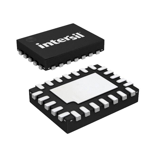
The ISL15102 is supplied in a thermally-enhanced small
footprint (4mmx5mm) 24 Ld QFN package. The
ISL15102 is specified for operation across the -40°C to
+85°C operating ambient temperature range.
Table 1. Alternate Solutions
Part #
Nominal ±VS
(V)
Bandwidth
(MHz)
ISL15100
±6, +12
180
Broadband PLC
Related Literature
ISL1571
±6, +12
250
Broadband PLC
For a full list of related documents, visit our website
ISL15110
±6, +12
120
MIMO PLC
Applications
• ISL15102 product page
+12V
ISL15102
INA
VOUTA
CM Buffer
Vs
3k
RS
2.49
100nF
-
50
VINA-
100k
RF
4.22k
1:1
100
VCM
AFE
+12V
A = 10
VINA+
+
100nF
VS+
50
RG
931
100nF
3k
RL
Line
VINB-
100k
+12V
100nF
-
VOUTB
RF
4.22k
100nF
VINB+
INB
+
RS
2.49
50
Bias Current
Control
DIS
Thermal
Shutdown
GND
Figure 1. Typical Application Circuit
FN8823 Rev.1.00
May 3, 2018
Page 1 of 16
�ISL15102
1.
1. Overview
Overview
1.1
Ordering Information
Part Number
(Notes 2, 3)
Part
Marking
Operating Ambient
Temp Range (°C)
Tape and Reel
(Units) (Note 1)
Package
(RoHS Compliant)
Pkg.
Dwg. #
ISL15102IRZ
15102IRZ
-40 to +85
-
24 Ld QFN
L24.4x5F
ISL15102IRZ-T13
15102IRZ
-40 to +85
2.5k
24 Ld QFN
L24.4x5F
ISL15102IRZ-EVALZ
Notes:
1. Refer to TB347 for details about reel specifications.
2. These Pb-free plastic packaged products employ special Pb-free material sets, molding compounds/die attach materials, and
100% matte tin plate plus anneal (e3 termination finish, which is RoHS compliant and compatible with both SnPb and Pb-free
soldering operations). Pb-free products are MSL classified at Pb-free peak reflow temperatures that meet or exceed the Pb-free
requirements of IPC/JEDEC J STD-020.
3. For Moisture Sensitivity Level (MSL), see the ISL15102 product information page. For more information about MSL, refer to
TB363.
Pin Configuration
ISL15102
(24 Ld QFN)
VINA+ 1
+
-
VINB+ 2
20 VOUTA
21 VS+
22 GND
24 NC
23 DIS
Top View
20 VOUTA
21 VS+
22 GND
23 DIS
24 NC
Internal View
19 VINA-
VINA+ 1
19 VINA-
18 VINB-
VINB+ 2
18 VINB-
17 VOUTB
NC 3
16 NC
NC 4
VCM 5
15 NC
VCM 5
15 NC
NC 6
14 NC
NC 6
14 NC
NC 7
13 NC
NC 7
13 NC
FN8823 Rev.1.00
May 3, 2018
17 VOUTB
16 NC
NC 12
VS+ 11
GND 10
THERMAL
PAD
NC 9
NC 12
VS+ 11
NC 9
NC 8
NC 4
GND 10
+
8
NC 3
NC
1.2
Page 2 of 16
�ISL15102
1. Overview
1.3
Pin Descriptions
Pin Number
Pin Name
1
VINA+
Amplifier A non-inverting input
Function
Refer to Circuit 1
Circuit
2
VINB+
Amplifier B non-inverting input
Refer to Circuit 1
3, 4, 6, 7, 8, 9, 12, 13,
14, 15, 16, 24
NC
10, 22
GND
Ground connection
5
VCM
Output common-mode bias
11, 21
VS+
Positive supply voltage
17
VOUTB
18
No internal connection
Amplifier B output
Refer to Circuit 2
VINB-
Amplifier B inverting input
Refer to Circuit 3
19
VINA-
Amplifier A inverting input
Refer to Circuit 3
20
VOUTA
Amplifier A output
Refer to Circuit 2
23
DIS
Disable control pin
-
Thermal Pad
Connects to GND
VS+
VS+
VS+
GND
GND
GND
VS+
GND
Circuit 1
FN8823 Rev.1.00
May 3, 2018
Circuit 2
Circuit 3
Page 3 of 16
�ISL15102
2.
2. Specifications
Specifications
2.1
Absolute Maximum Ratings
TA = +25°C
Parameter
Minimum
Maximum
Unit
VS+ Voltage to GND
-0.3
30
V
Driver VIN+ Voltage
GND
VS+
V
DIS Voltage to GND
-0.3
6
V
VCM Voltage to GND
GND
VS+
ESD Rating
Human Body Model (Tested per JS-001-2014)
Charged Device Model (Tested per JS-002-2014)
Value
Unit
2
kV
750
V
CAUTION: Do not operate at or near the maximum ratings listed for extended periods of time. Exposure to such conditions may
adversely impact product reliability and result in failures not covered by warranty.
2.2
Thermal Information
Thermal Resistance (Typical)
24 Ld QFN Package (Notes 4, 5)
JA (°C/W)
JC (°C/W)
38
4
Notes:
4. JA is measured in free air with the component mounted on a high-effective thermal conductivity test board with “direct attach”
features. See TB379.
5. For JC, the “case temp” location is the center of the exposed metal pad on the package underside.
Parameter
Storage Temperature Range
Minimum
Maximum
Unit
-65
+150
°C
Power Dissipation
See Figure 14 on page 9
Pb-Free Reflow Profile
2.3
Refer to TB493
Recommended Operation Conditions
Parameter
Minimum
Maximum
Unit
Temperature Range
-40
+85
°C
Junction Temperature
-40
+150
°C
FN8823 Rev.1.00
May 3, 2018
Page 4 of 16
�ISL15102
2.4
2. Specifications
Electrical Specifications
Unless otherwise noted, all tests are at the specified temperature TA = +25°C, VS+ = +12V, AV = 10V/V, RF = 4.22kΩ, RL = 50Ω
differential, DIS = 0V.
Min
Typ
Max
(Note 6) (Note 7) (Note 6)
Unit
90
MHz
VO = 10VP-P-DIFF
60
MHz
VO = 10VP-P-DIFF
900
V/µs
2nd
Harmonic
VOUT = 2VP-P-DIFF
-88
dBc
3rd Harmonic
VOUT = 2VP-P-DIFF
-92
dBc
THD
VOUT = 2VP-P-DIFF
-86
dBc
2nd
Harmonic
VOUT = 2VP-P-DIFF
-83
dBc
3rd Harmonic
VOUT = 2VP-P-DIFF
-70
dBc
THD
VOUT = 2VP-P-DIFF
-70
dBc
2nd
Harmonic
VOUT = 2VP-P-DIFF
-76
dBc
3rd Harmonic
VOUT = 2VP-P-DIFF
-66
dBc
Parameter
Symbol
Test Conditions
AC Performance
-3dB Small Signal Bandwidth
BW
-3dB Large Signal Bandwidth
20% to 80%
200kHz Harmonic Distortion
3MHz Harmonic Distortion
6MHz Harmonic Distortion
SR
VO < 2VP-P-DIFF
VOUT = 2VP-P-DIFF
-65
dBc
Non-Inverting Input Voltage Noise at each of
the Two Inputs
eN
f = 1MHz
8.5
nV/Hz
Non-Inverting Input Current Noise at each of
the Two Inputs
+iN
f = 1MHz
1.5
pA/Hz
Inverting Input Current Noise at each of the
Two Inputs
-iN
f = 1MHz
38
pA/Hz
eN-CM
f = 1MHz
128
nV/Hz
THD
Common-Mode Output Noise
Power Control Features
Logic High Voltage
VIH
DIS input
Logic Low Voltage
VIL
DIS input
2.0
V
Logic High Current for DIS
IIH
DIS = 3.3V
0.3
µA
Logic Low Current for DIS
IIL
DIS = 0V
-0.4
µA
Maximum Operating Supply Voltage
28
V
Minimum Operating Supply Voltage
8
V
All outputs at 0V, DIS = 3.3V
0.4
mA
All outputs at VS+/2, DIS = 0V
VO-Diff = 0V
21
mA
0.4
mA
20
VP-P
0.8
V
Supply Characteristics
GND Pin Current
Positive Supply Current
Positive Supply Current
IGND
IS+
(full power)
All outputs at VS+/2,
IS+
(power-down) DIS = 3.3V, VO-Diff = 0V
Output Characteristics
VOUT
RL-DIFF = no load
Input Offset Voltage - Differential Mode
VIOS-DM
(VINA+ - VINB+)
-17
-0.3
17
mV
Input Offset Voltage - Common-Mode
VIOS-CM
Delta to VS+/2
-17
4
17
mV
Unloaded Output Differential Swing
Input Characteristics
FN8823 Rev.1.00
May 3, 2018
Page 5 of 16
�ISL15102
2. Specifications
Unless otherwise noted, all tests are at the specified temperature TA = +25°C, VS+ = +12V, AV = 10V/V, RF = 4.22kΩ, RL = 50Ω
differential, DIS = 0V. (Continued)
Parameter
Input VOS Drift
Non-Inverting Input Bias Current - Differential
Mode
Inverting Input Bias Current - Differential Mode
Symbol
VOS, DRIFT
Test Conditions
Min
Typ
Max
(Note 6) (Note 7) (Note 6)
Unit
±2
µV/°C
-25°C to +125°C TJ
+IBDM
(+IBA - +IBB)
-3
0.2
3
-IBDM
(-IBA - -IBB)
-20
-0.6
20
µA
µA
Non-Inverting IB+ Drift
IB+, DRIFT
-25°C to +85°C TJ
±6
nA/°C
Inverting IB- Drift
IB-, DRIFT
-25°C to +85°C TJ
±6
nA/°C
PSRR
VS+ = +8V to +28V
68
dB
VS+ = +8V to +28V
22
dB
6
kΩ
+160
°C
Power Supply Rejections to Differential Output
(Input Referred)
Power Supply Rejections to Common-Mode
Output (Output Referred)
Differential Input Resistance
ZIN
Thermal Protection
Thermal Shutdown
+125
Notes:
6. Compliance to datasheet limits is assured by one or more methods: production test, characterization, and/or design.
7. Typical values are for information purposes only.
FN8823 Rev.1.00
May 3, 2018
Page 6 of 16
�ISL15102
3.
3. Typical Performance Curves
Typical Performance Curves
VS+ = +12V, RF = 4.22kΩ, AV = 10V/V differential, RL = 50Ω differential, TA = +25°C, DIS = 0V, unless otherwise noted.
5
20
VL = 2VP-P
RF = 4.22k:
-10
-15
-20
-25
-30
0
-10
-20
A = 10
A = 40
-35
1M
10M
Frequency (Hz)
VOUT = 0.5VP-P
VOUT = 10VP-P
A = 20
100M
1M
300M
10M
300M
100M
Frequency (Hz)
Figure 2. Small Signal Frequency Response vs Gain
Figure 3. Large Signal Frequency Response
-55
-70
-75
Harmonic Distortion (dBc)
RL = 50k:
-80
-85
-90
-95
HD2
-100
HD3
-105
RL = 50k:
-60
-65
-70
-75
-80
-85
HD2
-90
HD3
-95
0.1
1.0
10.0
0.1
20.0
Differential Output Voltage (VP-P)
1.0
10.0
20.0
Differential Output Voltage (VP-P)
Figure 4. 1MHz Harmonic Distortion vs Output Swing
Figure 5. 4MHz Harmonic Distortion vs Output Swing
-30
-30
VL = 1VP-P
-40
Harmonic Distortion (dBc)
Harmonic Distortion (dBc)
VOUT = 5VP-P
-30
-40
Harmonic Distortion (dBc)
RF = 4.22k:
A = 10
10
Gain (dB)
Normalized Gain (dB)
0
-5
-50
-60
-70
-80
-90
-100
HD2
HD3
VL = 1VP-P
-40
-50
-60
-70
-80
-90
-100
HD2
HD3
-110
-110
1
10
100
Differential Load (Ω)
Figure 6. 1MHz Harmonic Distortion vs Load
FN8823 Rev.1.00
May 3, 2018
200
1
10
100
200
Differential Load (Ω)
Figure 7. 4MHz Harmonic Distortion vs Load
Page 7 of 16
�ISL15102
3. Typical Performance Curves
VS+ = +12V, RF = 4.22kΩ, AV = 10V/V differential, RL = 50Ω differential, TA = +25°C, DIS = 0V, unless otherwise noted. (Continued)
30
30
A = 10
VL = 2VP-P
25
20
Gain (dB)
Gain (dB)
20
15
10
15
10
5
5
RF = 2800:
0
RF = 3480:
RF = 4220:
0
CL = 0pF
CL = 10pF
CL = 22pF
CL = 33pF
CL = 47pF
RF = 6340:
-5
-5
1M
10M
Frequency (Hz)
100M
1M
300M
10M
100M
300M
Frequency (Hz)
Figure 8. Small Signal Frequency Response vs RF
Figure 9. Small Signal Frequency Response vs CLOAD
30
0
A = 10
VL = 2VP-P
-10
Harmonic Distortion (dBc)
25
20
Gain (dB)
A = 10
VL = 2VP-P
25
15
10
RS = 1 : , CL = 47pF
RS = 2.5 : , CL = 47pF
RS = 10 : , CL = 47pF
RS = 25 : , CL = 47pF
5
0
10M
Frequency (Hz)
HD2
HD3
-20
-30
-40
-50
-60
-70
-80
-90
100k
0M
-5
1M
A = 10
VL = 0.75VP-P
100M
300M
1M
10M
50M
Frequency (Hz)
Figure 10. Small Signal Frequency Response vs RS
and CLOAD
Figure 11. Harmonic Distortion vs Frequency
5
25
20
0
-5
Gain (dB)
Gain (dB)
15
-10
-15
A = 10
VL = 2VP-P
10
5
0
CL = 0pF
CL = 10pF
-5
CL = 22pF
CL = 33pF
-10
VS = 8V
CL = 47pF
-20
VS = 18V
VS = 28V
-15
1M
10M
100M
300M
Frequency (Hz)
Figure 12. Common-Mode Small Signal Frequency
Response vs CLOAD
FN8823 Rev.1.00
May 3, 2018
1M
10M
Frequency (Hz)
100M
300M
Figure 13. Small Signal Frequency Response vs Supply
Voltage
Page 8 of 16
�ISL15102
3. Typical Performance Curves
VS+ = +12V, RF = 4.22kΩ, AV = 10V/V differential, RL = 50Ω differential, TA = +25°C, DIS = 0V, unless otherwise noted. (Continued)
4.0
3.38W
Power Discipation (W)
3.5
3.0
4JA = +39°C/W
2.5
2.0
1.5
1.0
0.5
0.0
0
25
50
75
100
Ambient Temperature (°C)
125
150
Figure 14. Package Power Dissipation vs Ambient Temperature
FN8823 Rev.1.00
May 3, 2018
Page 9 of 16
�ISL15102
4.
4. Test Circuit
Test Circuit
A
R
Network
Analyzer
+12
S
DC
Splitter
50Ω
487Ω
DUT
180°
Splitter
RL
1:1
50Ω
Load
53Ω
487Ω
50Ω
Figure 15. Frequency Response Characterization Circuit
FN8823 Rev.1.00
May 3, 2018
Page 10 of 16
�ISL15102
5.
5. Applications Information
Applications Information
5.1
Applying Wideband Current Feedback Op Amps as Differential Drivers
A Current Feedback Amplifier (CFA) such as the ISL15102 is particularly suited to the requirements of high output
power, high bandwidth, and differential drivers. This topology offers a high slew rate on low quiescent power and
the ability to hold AC characteristics relatively constant over a wide range of gains. The AC characteristics are
principally set by the feedback resistor (RF) value in simple differential gain circuits as shown in Figure 16.
+12V
+
-
50
RS, 2.49
ISL15102
RF, 4.22k
RG, 931
VI
Load
VO
RF, 4.22k
RS, 2.49
ISL15102
+
50
VO/VI = 10V/V
Figure 16. Passive Termination Circuit
In this differential gain of 10V/V circuit, the 4.22k feedback resistors (RF) set the bandwidth, and the 931 gain
resistor (RG) controls the gain. The VO/VI gain for this circuit is set by Equation 1:
VO
R
4.22kΩ
-------- = 1 + 2 -------F- = 1 + 2 ------------------- = 10.06
VI
931Ω
R G
(EQ. 1)
The effect of increasing or decreasing the feedback resistor value is shown in Figure 8 on page 8. Increasing RF
will tend to roll off the response, while decreasing it will peak the frequency response up, extending the bandwidth.
RG was adjusted in each of these plots to hold a constant gain of 10 (or 20dB). This shows the flexibility offered by
the CFA topology; the frequency response can be controlled with the value of the feedback resistor, RF, with
resistor RG setting the desired gain.
The ISL15102 provides two very power efficient, high output current CFAs. These are intended to be connected as
one differential driver. The “Pin Configuration” on page 2 show that Channels A and B are intended to operate as a
pair. Power-down control is provided through control pin DIS, which sets the power for Channels A and B together.
Very low output distortion at low power can be provided by the differential configuration. The high slew rate
intrinsic to the CFA topology also contributes to the exceptional performance shown in Figure 11 on page 8. This
swept frequency distortion plot shows low distortion at 200kHz holding to very low levels up through 10MHz.
5.2
Input Biasing and Input Impedance
The ISL15102 has internal resistors at the non-inverting inputs for mid-rail biasing, so only external AC coupling
capacitors are required for input biasing, shown in Figure 1 on page 1. With a 100nF coupling capacitor and an
input differential impedance of 6kΩ typical, the first order high-pass cut-off frequency is 530Hz.
FN8823 Rev.1.00
May 3, 2018
Page 11 of 16
�ISL15102
5.3
5. Applications Information
Power Control Function
DIS controls the quiescent current for the port constructed from Amplifiers A and B. Taking DIS high (>2V), will
put the device in Power-Down mode, reducing the supply current to typical 0.4mA. Taking DIS low (


 工商网监
湘ICP备2023018690号
工商网监
湘ICP备2023018690号
