DATASHEET
ISL1591
FN7625
Rev 1.00
October 31, 2012
Fixed Gain, Dual Port, VDSL2 Line Driver
The ISL1591 provides 4 internal wideband op amps intended
to be used as two pairs of fixed gain differential line drivers.
The ISL1591’s high bandwidth, and ultra low distortion
enables the support of VDSL2 8b, 17a, and 30a in central
office modem applications. This highly versatile line driver
allows for operation from +14V to +24V nominal power
supplies, while delivering exceptional MTPR distortion
performance.
Features
Using a single +24V supply, the ISL1591 MBPR distortion is
below -62dBc in VDSL2 8b, -63dBc in VDSL2 17a, and -60dBc
in VDSL2 30a profiles. Using a single +14V supply, ISL1591
supports 14.5dBm VDSL2 17a and 30a profiles at only a
power consumption of 425mW. This capability is ideal for
short loop, high bit rate VDSL2 applications where 14.5dBm
transmit power is all that is required. For full power VDSL2 8b
profile with 20dBm of transmit power, the line driver will
require +24V single supply.
• -64dBc US1, -62dBc US2, -60dBc US3 MBPR (VDSL 30a
Profile)
Each of the 4 internal op amps is a wideband current feedback
amplifier offering very high slew rate intrinsic to that design
using low quiescent current levels. Each of the two pair of
amplifiers (ports) can also be power optimized to the
application using two external quiescent control logic pins. Full
power is nominally 14mA/port with options of medium power
cutback to 9.7mA/port, a low power condition at 7.4mA/port,
and an off state at 360mA peak output current. Driving differentially, this gives
>42.4VP-P swing to as low as 58 differential load. The four
amplifiers in ISL1591 are intended to be used as differential
pairs and not as individual amplifiers.
• Internal Fixed Gain of 11.6V/V at RLOAD
• ±360mA Output Drive Capability
• 42.4VP-P Differential Output Drive into 82.6
• -62dBc MBPR (VDSL 8b Profile)
• -65dBc US1, -63dBc US2 MBPR (VDSL2 17a Profile)
• High Slew Rate of 2000V/µs Differential
• Bandwidth (170MHz)
• Supply Current Control Pins
• K.20, GR-1089 Surge Robustness Validated
• Pb-Free (RoHS Compliant)
• ADSL2+
• VDSL2 Profiles: 8MHz, 17MHz, and 30MHz
Related Literature
• AN1325 “Choosing and Using Bypass Capacitors”
TABLE 1. ALTERNATE SOLUTIONS
PART #
±6,+12
200
VDSL2
±12,+24
50
ADSL2+
ISL1539A
±12,+24
240
VDSL2
10
0
1:N
1/2
Vo
ISL1591
Rb
Rb = 100 x 0.2 x 0.5
N2
Vo
= 11.6 V V
Vi
FIGURE 1. FIXED GAIN LINE DRIVER CIRCUIT
FN7625 Rev 1.00
October 31, 2012
PAR = 5.4
20.2dBm
Avg. US1 MTBR = -65dBc
-20
100
LINE
MBPR (dB)
Rb
VCM
APPLICATIONS
ISL1557
-10
Vi
BANDWIDTH
(MHz)
ISL1536
+24V
AFE
NOMINAL ±VCC
(V)
-30
-40
-50
-60
-70
-80
-90
3.75M
4.15M
4.55M
FREQUENCY (Hz)
4.95M
5.35M
FIGURE 2. MBPR VDSL2 8b PERFORMANCE
Page 1 of 18
�ISL1591
+VS
+
Connection Diagram
VIN
+
Rt
3k
VOUT
¼
ISL1591
Rb
8.25
+VS
AFE
VCM
Rf
1.31k
Rc
100k
1:n
Rp
1.78k
Rg
Rc 736
100k
Rp
1.78k
Rf
1.31k
FB
Line
FB
-
¼
ISL1591
VOUT
Rb
8.25
Rt
3k
+
VIN
BIAS
CURRENT
CONTROL
C0
C1
GND
FIGURE 3. TYPICAL DIFFERENTIAL I/O LINE DRIVER (1 OF 2 PORTS)
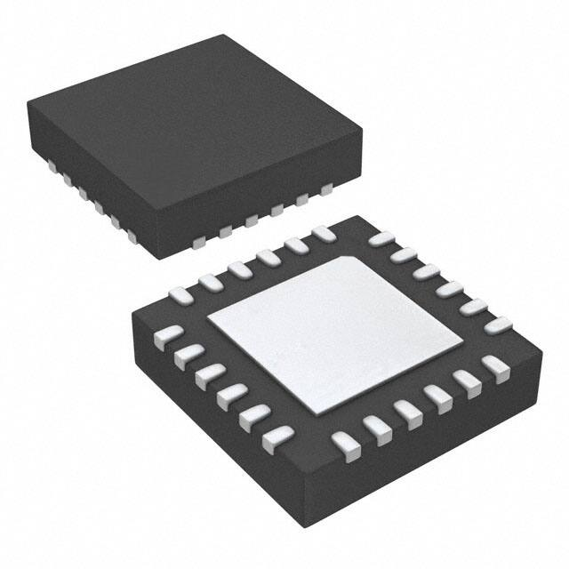
Pin Configuration
19 FBB
20 VOUTB
21 VOUTA
22 FBA
23 C0AB
24 C1AB
ISL1591
(24 LD TQFN)
TOP VIEW
VINA+ 1
18 +VS
VINB+ 2
17 DNC
VCMAB 3
16 DNC
THERMAL
PAD
VCMCD 4
15 DNC
FBC 12
VOUTC 11
VOUTD 10
FBD 9
13 GND
C0CD 8
14 DNC
C1CD 7
VINC+ 5
VIND+ 6
THERMAL PAD CONNECTS TO GND
FN7625 Rev 1.00
October 31, 2012
Page 2 of 18
�ISL1591
Pin Descriptions
PIN NUMBER
PIN NAME
1
VINA+
Amplifier A non-inverting input
FUNCTION
2
VINB+
Amplifier B non-inverting input
3
VCMAB
Input common mode bias for port AB(#1)
4
VCMCD
Input common mode bias for port CD(#2)
5
VINC+
Amplifier C non-inverting input
6
VIND+
Amplifier D non-inverting input
7
C1CD
DSL Port #2 current control pin
8
C0CD
9
FBD
10
VOUTD
Amplifier D output
11
VOUTC
Amplifier C output
DSL Port #2 current control pin
Feedback pin for amplifier D
12
FBC
Feedback pin for amplifier C
13
GND
Ground
14, 15, 16, 17
DNC
Do not connect
18
+VS
Positive supply voltage
19
FBB
Feedback pin for amplifier B
20
VOUTB
21
VOUTA
22
FBA
Amplifier B output
Amplifier A output
Feedback pin for amplifier A
23
C0AB
DSL Port #1 current control pin
24
C1AB
DSL Port #1 current control pin
-
THERMAL PAD
Connects to GND
Ordering Information
PART
NUMBER
(Notes 2, 3)
PART
MARKING
TEMP RANGE
(°C)
PACKAGE
(Pb-free)
PKG.
DWG. #
ISL1591IRTZ
15 91IRTZ
-40 to +85
24 Ld TQFN
L24.4x4F
ISL1591IRTZ-T7 (Note 1)
15 91IRTZ
-40 to +85
24 Ld TQFN
L24.4x4F
ISL1591IRTZ-T13 (Note 1)
15 91IRTZ
-40 to +85
24 Ld TQFN
L24.4x4F
ISL1591IRTZ-EVALZ
Evaluation Board
NOTES:
1. Please refer to TB347 for details on reel specifications.
2. These Intersil Pb-free plastic packaged products employ special Pb-free material sets, molding compounds/die attach materials, and 100% matte
tin plate plus anneal (e3 termination finish, which is RoHS compliant and compatible with both SnPb and Pb-free soldering operations). Intersil
Pb-free products are MSL classified at Pb-free peak reflow temperatures that meet or exceed the Pb-free requirements of IPC/JEDEC J STD-020.
3. For Moisture Sensitivity Level (MSL), please see device information page for ISL1591. For more information on MSL please see tech brief TB363.
FN7625 Rev 1.00
October 31, 2012
Page 3 of 18
�ISL1591
Absolute Maximum Ratings (TA = +25°C)
Thermal Information
VS+ Voltage to GND . . . . . . . . . . . . . . . . . . . . . . . . . . . . . . . . -0.3V to +26.4V
Driver VIN+ Voltage. . . . . . . . . . . . . . . . . . . . . . . . . . . . . . . . . . . . .GND to VS+
C0, C1 Voltage to GND . . . . . . . . . . . . . . . . . . . . . . . . . . . . . . . . . -0.3V to +6V
VCM Voltage to GND . . . . . . . . . . . . . . . . . . . . . . . . . . . . . . . . . . . .GND to VS+
Current into any Input . . . . . . . . . . . . . . . . . . . . . . . . . . . . . . . . . . . . . . . 8mA
Continuous Output Current for Long Term Reliability. . . . . . . . . . . . . . . . .50mA
ESD Rating
Human Body Model (Tested per JESD22-A114F). . . . . . . . . . . . . . . . . . 3kV
Machine Model (Tested per JESD22-A115C) . . . . . . . . . . . . . . . . . . 300V
Charge Device Model (Tested per JESD22-C101E). . . . . . . . . . . . . .1.5kV
Thermal Resistance (Typical)
JA (°C/W) JC (°C/W)
24 Ld TQFN Package (Notes 4, 5) . . . . . . .
43
5.5
Maximum Junction Temperature (Plastic Package) . . . . . . . . . . . .+150°C
Power Dissipation . . . . . . . . . . . . . . . . . . . . . . . . . . . . . . . . . . . . . . . . See Figure 47
Storage Temperature Range. . . . . . . . . . . . . . . . . . . . . . . .-40°C to +150°C
Pb-Free Reflow Profile . . . . . . . . . . . . . . . . . . . . . . . . . . . . . . . see link below
http://www.intersil.com/pbfree/Pb-FreeReflow.asp
Operating Conditions
Ambient Temperature Range . . . . . . . . . . . . . . . . . . . . . . . . -40°C to +85°C
Junction Temperature Range . . . . . . . . . . . . . . . . . . . . . . .-40°C to +150°C
CAUTION: Do not operate at or near the maximum ratings listed for extended periods of time. Exposure to such conditions may adversely impact product
reliability and result in failures not covered by warranty.
NOTES:
4. JA is measured in free air with the component mounted on a high effective thermal conductivity test board with “direct attach” features. See Tech
Brief TB379.
5. For JC, the “case temp” location is the center of the exposed metal pad on the package underside.
IMPORTANT NOTE: All parameters having Min/Max specifications are guaranteed. Typ values are for information purposes only. Unless otherwise noted,
all tests are at the specified temperature and are pulsed tests, therefore: TJ = TC = TA
Electrical Specifications
unless otherwise indicated.
PARAMETER
VS = +24V, RL= 82.6differential, C0 = C1 = 0V, TA = +25°C. Amplifier pairs tested separately,
DESCRIPTION
CONDITIONS
MIN
(Note 6)
TYP
MAX
(Note 6)
UNIT
11.1
11.6
12.1
V/V
AC PERFORMANCE
Av
Internal Gain Across RLOAD
RB = 8.25
BW
-3dB Small Signal Bandwidth
VO < 2VP-P-DIFF
-3dB Large Signal Bandwidth
VO = 10VP-P-DIFF
SR
20% to 80%
VO = 32VP-P-DIFF
200kHz Harmonic
Distortion
2nd Harmonic
VOUT = 2VP-P-DIFF
-90
-80
dBc
VOUT = 10VP-P-DIFF
-87
-78
dBc
VOUT = 2VP-P-DIFF
-90
-78
dBc
VOUT = 10VP-P-DIFF
-87
-80
dBc
VOUT = 2VP-P-DIFF
-87
-76
dBc
VOUT = 10VP-P-DIFF
-84
-76
dBc
3rd Harmonic
THD
170
1800
MHz
60
MHz
2000
V/µs
2nd Harmonic
VOUT = 10VP-P-DIFF
-83
dBc
3rd Harmonic
VOUT = 10VP-P-DIFF
-75
dBc
THD
VOUT = 10VP-P-DIFF
-74
dBc
2nd Harmonic
VOUT = 2VP-P-DIFF
-73
dBc
3rd Harmonic
VOUT = 2VP-P-DIFF
-65
dBc
THD
VOUT = 2VP-P-DIFF
-65
dBc
MBPR
Missing-Band Power Ratio: US1
Band
26kHz to 8MHz, 4kHz Tone Spacing,
PLINE = 19dBm, VDSL2+ 8b
-65
eO
Output Voltage Noise
f = 1MHZ
90
nV/Hz
eN-CM
Common Mode Output Noise at
each Port Pair
f = 1MHZ
90
nV/Hz
4MHz Harmonic
Distortion
8MHz Harmonic
Distortion
-62
dBc
POWER CONTROL FEATURES
VIH
FN7625 Rev 1.00
October 31, 2012
Logic High Voltage
C0 and C1 inputs
2.0
V
Page 4 of 18
�ISL1591
Electrical Specifications
unless otherwise indicated. (Continued)
PARAMETER
VS = +24V, RL= 82.6differential, C0 = C1 = 0V, TA = +25°C. Amplifier pairs tested separately,
DESCRIPTION
CONDITIONS
MIN
(Note 6)
TYP
MAX
(Note 6)
UNIT
0.8
V
VIL
Logic Low Voltage
C0 and C1 inputs
IIH0 , IIH1
Logic High Current for C0, C1
C0 = 3.3V, C1 = 3.3V
-7.5
1
+7.5
µA
IIL0, IIL1
Logic Low Current for C0, C1
C0 = 0V, C1 = 0V
-17
-13
-10
µA
SUPPLY CHARACTERISTICS
Maximum Operating Supply
Voltage
+25.2
V
Minimum Operating Supply
Voltage
+14
V
IS+ (Full Power)
Positive Supply Current per Port
IS+ (Medium)
Positive Supply Current per Port
14.9
mA
10.8
12
mA
9.7
10.5
mA
6.7
7.2
8.0
mA
All outputs at VCM, C0 = 0V, C1 = 3.3V,
+VS = 24V
6.8
7.4
8.1
mA
+VS = 14V
5.0
5.4
6.1
mA
All outputs at VCM, C0 = C1 = 3.3V,
+VS = 24V
0.4
0.5
0.65
mA
+VS = 14V
0.3
0.4
0.5
mA
Output Swing
RL-DIFF = No Load
+22
+22.4
V
Lightly Loaded Output Swing
RL-DIFF = 100
+20.2
+21.2
V
IOL
Linear Output Current
RL = 25, f = 100kHz, THD = -60dBc
±360
mA
IOUT
Peak Output Current
VOUT = ±1V, RL = 1
±600
mA
VOS-OUT
Differential Output Offset Voltage
-150
25
+150
mV
VOS-CM
Common Mode Output Offset
Voltage
-50
-20
+50
mV
+19.5
V
IS+ (Low)
IS+ (Power-down)
Positive Supply Current per Port
Positive Supply Current per Port
All outputs at VCM, C0 = C1 = 0V, +VS = 24V
13
14
+VS = 14V
9.7
All outputs at VCM, C0 = 3.3V, C1 = 0V,
+VS = 24V
9.1
+VS = 14V
OUTPUT CHARACTERISTICS
VOUT
INPUT CHARACTERISTICS
+4.5
CMIR
Common Mode Input Range at
each of the 4 Non-Inverting Input
Pins
CMRR
Common Mode Rejections for
VCM to Differential Mode Output (Input
each Port. VCM = +4.5V to +19.5V Referred), DC
66
dB
VCM to Commonl Mode Output (Output
Referred), DC
55
dB
Power Supply Rejections for each +VS = +15V to +24V, GND = 0V, DC
Port to Differential Output (Input
Referred)
66
dB
Power Supply Rejections for each +VS = +15V to +24V, GND = 0V, DC
Port to Common Mode Output
(Output Referred)
58
dB
Input Resistance
6.0
k
PSRR
RIN
Differential
NOTE:
6. Compliance to datasheet limits is assured by one or more methods: production test, characterization and/or design.
FN7625 Rev 1.00
October 31, 2012
Page 5 of 18
�ISL1591
Typical Performance Curves
VCC = +24V, Rb = 8.25, GND at the Load = 11.6V/V (differential),
RLOAD = 82.5, TA +25°C, C0 = C1 = 0V (full power) unless otherwise noted.
27
30
27
Rb = 6.2
21
18
Rb = 15
15
1VP-P
24
Rb = 8.25
GAIN (dB)
GAIN (dB)
24
12
21
2VP-P
18
5VP-P
10VP-P
20VP-P
15
9
6
100k
1M
10M
FREQUENCY (Hz)
100M
12
1G
-30
-40
-40
-50
-50
DISTORTION (dBc)
DISTORTION (dBc)
-30
3rd HD dBc
-70
THD dBc
-80
-90
-100
5
10
15
20
25
30
OUTPUT AMPLITUDE AT LOAD (VP-P(-d))
100M
1G
THD dBc
-80
2nd HD dBc
3rd HD dBc
0
5
10
15
20
25
VOP-P(-d) AT THE LOAD
30
35
FIGURE 7. 4MHz HARMONIC DISTORTION vs OUTPUT AMPLITUDE
-30
-30
HARMONIC DISTORTION (dBc)
-40
DISTORTION (dBc)
10M
FREQUENCY (Hz)
-70
-100
35
FIGURE 6. 1MHz HARMONIC DISTORTION vs OUTPUT AMPLITUDE
-50
THD dBc
-60
-70
-80
2nd HD dBc
3rd HD dBc
-90
-100
-60
-90
2nd HD dBc
0
1M
FIGURE 5. LARGE SIGNAL FREQUENCY RESPONSE
FIGURE 4. SMALL SIGNAL FREQUENCY RESPONSE vs GAIN AT
THE LOAD
-60
100k
0
5
10
15
20
25
30
OUTPUT AMPLITUDE AT LOAD (VOP-P(-d))
35
FIGURE 8. 8MHz HARMONIC DISTORTION vs OUTPUT AMPLITUDE
FN7625 Rev 1.00
October 31, 2012
5VOP-P
-40
3rd HD dBc
-50
THD dBc
-60
-70
2nd HD dBc
-80
-90
-100
0
2M
4M
6M
8M 10M 12M 14M 16M 18M 20M
FREQUENCY (Hz)
FIGURE 9. HARMONIC DISTORTION vs FREQUENCY
Page 6 of 18
�ISL1591
Typical Performance Curves
VCC = +24V, Rb = 8.25, GND at the Load = 11.6V/V (differential),
RLOAD = 82.5, TA +25°C, C0 = 3.3V, C1 = 0V (85% power) unless otherwise noted.
27
30
1VP-P
27
Rb = 6.2
Rb = 8.25
21
GAIN (dB)
GAIN (dB)
24
24
18
Rb = 15
15
2VP-P
21
5VP-P
10VP-P
18
20VP-P
12
15
9
6
100k
1M
10M
FREQUENCY (Hz)
100M
12
1G
-30
-30
-40
-40
-50
-50
-60
-70
THD dBc
3rd HD dBc
-80
-90
-100
5
10
15
20
25
30
OUTPUT AMPLITUDE AT LOAD (VP-P(-d))
2nd HD dBc
-80
3rd HD dBc
0
5
10
15
20
25
VOP-P(-d) AT THE LOAD
30
35
HARMONIC DISTORTION (dBc)
-30
-40
DISTORTION (dBc)
1G
FIGURE 13. 4MHz HARMONIC DISTORTION vs OUTPUT AMPLITUDE
-30
-50
THD dBc
-60
2nd HD dBc
-70
3rd HD dBc
-80
-90
-100
100M
-70
-100
35
FIGURE 12. 1MHz HARMONIC DISTORTION vs OUTPUT AMPLITUDE
10M
FREQUENCY (Hz)
THD dBc
-60
-90
2nd HD dBc
0
1M
FIGURE 11. LARGE SIGNAL FREQUENCY RESPONSE
DISTORTION (dBc)
DISTORTION (dBc)
FIGURE 10. SMALL SIGNAL FREQUENCY RESPONSE vs GAIN AT
THE LOAD
100k
0
5
10
15
20
25
30
OUTPUT AMPLITUDE AT LOAD (VP-P(-d))
35
FIGURE 14. 8MHz HARMONIC DISTORTION vs OUTPUT AMPLITUDE
FN7625 Rev 1.00
October 31, 2012
5Vopp
-40
3rd HD dBc
-50
THD dBc
-60
-70
2nd HD dBc
-80
-90
-100
0
2M
4M
6M
8M 10M 12M 14M 16M 18M 20M
FREQUENCY (Hz)
FIGURE 15. HARMONIC DISTORTION vs FREQUENCY
Page 7 of 18
�ISL1591
Typical Performance Curves
VCC = +24V, Rb = 8.25, GND at the Load = 11.6V/V (differential),
RLOAD = 82.5, TA +25°C, C1 = 3.3V, C0 = 0V (50% power) unless otherwise noted.
27
30
1VP-P
27
Rb = 6.2
24
Rb = 8.25
21
18
Rb = 15
15
2VP-P
21
GAIN (dB)
GAIN (dB)
24
10VP-P
18
12
5VP-P
20VP-P
15
9
6
100k
1M
10M
FREQUENCY (Hz)
100M
12
1G
-30
-30
-40
-40
-50
-50
-60
THD dBc
-70
3rd HD dBc
-80
1M
10M
FREQUENCY (Hz)
100M
1G
FIGURE 17. LARGE SIGNAL FREQUENCY RESPONSE
DISTORTION (dBc)
DISTORTION (dBc)
FIGURE 16. SMALL SIGNAL FREQUENCY RESPONSE vs GAIN AT
THE LOAD
100k
THD dBc
-60
-70
2nd HD dBc
-80
3rd HD dBc
2nd HD dBc
-90
-100
0
5
10
15
20
25
30
OUTPUT AMPLITUDE AT LOAD (VP-P(-d))
-90
-100
35
FIGURE 18. 1MHz HARMONIC DISTORTION vs OUTPUT AMPLITUDE
10
15
20
25
VOP-P(-d) AT THE LOAD
30
35
-30
HARMONIC DISTORTION (dBc)
-40
DISTORTION (dBc)
5
FIGURE 19. 4MHz HARMONIC DISTORTION vs OUTPUT AMPLITUDE
-30
THD dBc
-50
2nd HD dBc
-60
-70
3rd HD dBc
-80
-90
-100
0
0
5
10
15
20
25
30
OUTPUT AMPLITUDE AT LOAD (VP-P(-d))
35
FIGURE 20. 8MHz HARMONIC DISTORTION vs OUTPUT AMPLITUDE
FN7625 Rev 1.00
October 31, 2012
5VO(P-P)
-40
3rd HD dBc
-50
THD dBc
-60
-70
2nd HD dBc
-80
-90
-100
0
2M
4M
6M
8M 10M 12M 14M 16M 18M 20M
FREQUENCY (Hz)
FIGURE 21. HARMONIC DISTORTION vs FREQUENCY
Page 8 of 18
�ISL1591
Typical Performance Curves
VCC = +24V, Rb = 8.25, GND at the Load = 11.6V/V (differential),
RLOAD = 82.5, TA +25°C, C0 = C1, C0 = 0V (Full power) unless otherwise noted.
30
6
CL = 22pF
27
24V
0
12V
-3
CL = 1pF
24
20V
GAIN (dB)
GAIN (dB)
3
14V
CL = 5pF
21
18
10V
15
-6
100k
1M
10M
FREQUENCY (Hz)
100M
FIGURE 22. SMALL SIGNAL BW vs SUPPLY VOLTAGE
GAIN (dB)
3
Rb = 8.25 with RLOAD = 82.5
100k
1M
10M
FREQUENCY (Hz)
100M
1G
FIGURE 23. SMALL SIGNAL FREQUENCY RESPONSE vs CLOAD
(AFTER RB)
900
82.5 RLOAD
800
Rb = 5.1 with RLOAD = 51
DIFFERENTIAL EO AT
82.5ohm LOAD (nV/√Hz)
6
12
1G
0
51 RLOAD
-3
-6
ALL POWER MODES
700
600
500
400
300
200
100
-9
100k
1M
10M
FREQUENCY (Hz)
100M
0
1k
1G
FIGURE 24. SMALL SIGNAL FREQUENCY RESPONSE vs RLOAD
10k
100k
1M
FREQUENCY (Hz)
10M
100M
FIGURE 25. OUTPUT VOLTAGE NOISE
10
PAR = 6.33
14.5dBm, RL = 51VS = +14V
AVG. US2 MTBR = -63dBc
0
MTBR (dB)
-10
-20
-30
-40
-50
-60
-70
-80
8.4M
8.9M
9.4M
9.9M
10.4M 10.9M
FREQUENCY (Hz)
11.4M
11.9M
FIGURE 26. VDSL2 17a PROFILE MTBR US2
FN7625 Rev 1.00
October 31, 2012
Page 9 of 18
�ISL1591
Typical Performance Curves
VCC = +24V, Rb = 8.25, GND at the Load = 11.6V/V (differential),
RLOAD = 82.5, TA +25°C, C0 = 3.3V, C1 = 0V (85%power) unless otherwise noted.
6
30
24V
27
CL = 22pF
CL = 47pF
0
12V
-3
CL = 1pF
24
20V
GAIN (dB)
GAIN (dB)
3
14V
CL = 5pF
21
18
10V
15
-6
100k
1M
10M
FREQUENCY (Hz)
100M
12
100k
1G
FIGURE 27. SMALL SIGNAL BW vs SUPPLY VOLTAGE
10M
FREQUENCY (Hz)
100M
1G
FIGURE 28. SMALL SIGNAL FREQUENCY RESPONSE vs CLOAD
(AFTER RB)
10
6
Rb = 8.25 with RLOAD = 82.5
Rb = 5.1 with RLOAD = 51
14.5dBm, PAR = 6.08
FULL POWER MODE
Avg US1 MTBR = -64dBc
0
82.5 RLOAD
-10
3
-20
MTBR (dB)
GAIN (dB)
1M
0
51 RLOAD
-30
-40
-50
-60
-3
-70
-80
-6
100k
1M
10M
FREQUENCY (Hz)
100M
-90
37M
1G
FIGURE 29. SMALL SIGNAL FREQUENCY RESPONSE vs R LOAD
43M 45M 47M
FREQUENCY (Hz)
49M
51M
10
14.5dBm, PAR = 6.08
FULL POWER MODE
Avg US2 MTBR = -62dBc
0
-10
-10
-20
-20
-30
-30
-40
-50
-40
-50
-60
-60
-70
-70
-80
-80
83M
93M
103M
113M
123M
FREQUENCY (Hz)
FIGURE 31. VDSL2 30a PROFILE MTBR US2
FN7625 Rev 1.00
October 31, 2012
133M
14.5dBm, PAR = 6.08
FULL POWER MODE
Avg US3 MTBR = -60dBc
0
MTBR (dB)
MTBR (dB)
41M
FIGURE 30. VDSL2 30a PROFILE MTBR US1
10
-90
39M
-90
21M
22M
23M
24M
FREQUENCY (Hz)
25M
FIGURE 32. VDSL2 30a PROFILE MTBR US3
Page 10 of 18
�ISL1591
Typical Performance Curves
VCC = +24V, Rb = 8.25, GND at the Load = 11.6V/V (differential),
RLOAD = 82.5, TA +25°C, C1 = 3.3V, C0 = 0V (50%power) unless otherwise noted.
30
6
24V
27
CL = 22pF
0
12V
CL = 47pF
24
20V
GAIN (dB)
GAIN (dB)
3
14V
CL = 1pF
21
CL = 5pF
18
10V
-3
15
-6
100k
1M
10M
FREQUENCY (Hz)
100M
12
1G
FIGURE 33. SMALL SIGNAL BW vs SUPPLY VOLTAGE
1M
10M
FREQUENCY (Hz)
100M
1G
FIGURE 34. SMALL SIGNAL FREQUENCY RESPONSE vs CLOAD
10
6
Rb = 8.25 with RLOAD = 82.5
82.5 RLOAD
0
Rb = 5.1 with RLOAD = 51
-10
3
PAR = 5.4
20.2dBm
Avg. US1 MTBR = -65dBc
-20
MTBR (dB)
GAIN (dB)
100k
0
51 RLOAD
-30
-40
-50
-60
-3
-70
-80
-6
100k
1M
10M
FREQUENCY (Hz)
100M
1G
FIGURE 35. SMALL SIGNAL FREQUENCY RESPONSE vs R LOAD
FN7625 Rev 1.00
October 31, 2012
-90
3.75M
4.15M
4.55M
FREQUENCY (Hz)
4.95M
5.35M
FIGURE 36. VDSL2+ 8b PROFILE MTBR
Page 11 of 18
�ISL1591
Typical Performance Curves
VCC = +24V, Rb = 8.25, GND at the Load = 11.6V/V (differential),
RLOAD = 82.5, TA +25°C, C0 and C1 Parametric unless otherwise noted.
9
0
-10
6
LOW POWER MODE
-20
FULL POWER MODE
-30
-40
0
GAIN (dB)
GAIN (dB)
3
MEDIUM POWER MODE
-50
-60
-70
-3
-80
-6
-100
-90
-110
-9
100k
1M
10M
FREQUENCY (Hz)
100M
1G
-120
100M
1M
10M
FREQUENCY (Hz)
100M
1G
FIGURE 38. CHANNEL-TO-CHANNEL X-TALK
FIGURE 37. COMMON MODE SMALL SIGNAL FREQUENCY
RESPONSE
2V/DIV
2V/DIV
5V/DIV
5V/DIV
100ns/DIV
500ns/DIV
FIGURE 39. POWER-UP TIME
FIGURE 40. POWER-DOWN TIME
0
-10
-20
-30
GAIN (dB)
-40
-50
-60
-70
-80
-90
-100
-110
-120
100M
1M
10M
FREQUENCY (Hz)
100M
1G
FIGURE 41. OFF-ISOLATION
FN7625 Rev 1.00
October 31, 2012
Page 12 of 18
�ISL1591
Typical Performance Curves
VCC = +24V, Rb = 8.25, GND at the Load = 11.6V/V (differential),
RLOAD = 82.5, TA +25°C, C0 and C1 Varied unless otherwise noted.
11.75
16
14
11.70
FULL POWER MODE
12
Iq (mA/PORT)
AV (V/V)
11.65
11.60
11.55
10
MEDIUM POWER MODE
8
6
LOW POWER MODE
4
11.50
11.45
2
-50 -40 -30 -20 -10 0
0
-50 -40 -30 -20 -10 0
10 20 30 40 50 60 70 80 90 100
TEMPERATURE (°C)
FIGURE 43. QUIESCENT CURRENT vs TEMPERATURE
-62
42.4
-63
42.3
MBPR (dBc)
DIFFERENTIAL OUTPUT SWING (VP-P)
FIGURE 42. GAIN AT THE LOAD vs TEMPERATURE
42.2
42.1
42.0
41.9
-65
-66
-67
-50 -40 -30 -20 -10 0
-68
-50 -40 -30 -20 -10 0
10 20 30 40 50 60 70 80 90 100
10 20 30 40 50 60 70 80 90 100
TEMPERATURE (°C)
FIGURE 44. DIFFERENTIAL OUTPUT SWING vs TEMPERATURE
FIGURE 45. 8b MBPR vs TEMPERATURE
10
5000
4500
5
SLEW RATE (V/µs)
DIFFERENTIAL OUTPUT (VOS)
FULL POWER MODE
8b VDSL2 SIGNAL
-64
TEMPERATURE (°C)
0
-5
-10
-15
-20
10 20 30 40 50 60 70 80 90 100
TEMPERATURE (°C)
4000
3500
3000
2500
2000
1500
-50 -40 -30 -20 -10 0
10 20 30 40 50 60 70 80 90 100
TEMPERATURE (°C)
FIGURE 46. OUTPUT OFFSET vs TEMPERATURE
FN7625 Rev 1.00
October 31, 2012
1000
-50 -40 -30 -20 -10 0
10 20 30 40 50 60 70 80 90 100
TEMPERATURE (°C)
FIGURE 47. SLEW RATE vs TEMPERATURE
Page 13 of 18
�ISL1591
Test Circuit
A
R
NETWORK
ANALYZER
+12
S
DC
SPLITTER
50
243
DUT
180°
SPLITTER
RL
50
LOAD
1:1
56
243
50
-12
FIGURE 48. FREQUENCY RESPONSE CHARACTERIZATION CIRCUIT
Applications Information
Applying Wideband Current Feedback Op
Amps as Differential Drivers
A current feedback amplifier (CFA) like the ISL1591 is
particularly suited to the requirements of high output power, full
power bandwidth, differential drivers. This topology offers a very
high slew rate on low quiescent power. The ISL1591 is a fixed
gain amplifier set to an optimized gain of 11.6V/V given
RL = 82.6 and Rb = 8.25, as shown in Figure 49.
The ISL1591 provides 4 very power efficient, high output current,
CFA's. These are intended to be connected as two pairs of
differential drivers. The “Connection Diagram” on page 2 shows
that Channels A and B are intended to operate as a pair while
Channels C and D comprise the other pair. Power control is also
provided through two pairs of control pins, which separately set
the power for Channels A and B together and then the other pair
controls Channels C and D together.
Advanced Configurations - Active
Termination
Where the best power efficiency is required in a full duplex DSL
line interface application, it is common to apply the circuit shown
in Figure 49 to reduce the power loss in the matching loads, Rb,
while retaining a higher impedance for the upstream signal
coming into this output stage. This circuit acts to provide a higher
apparent output impedance (through its cross-coupled positive
feedback through the Rp resistors integrated internally) while
physically taking a smaller IR drop through the Rb resistors for
the output signal.
Very low output distortion can be provided by the differential
configuration. The high slew rate intrinsic to the CFA topology
also contributes to the exceptional performance shown in
Figures 9, 15 and 21. These swept frequency distortion plots
show extremely low distortion at 200kHz holding to very low
levels up through 20MHz. At the full operating power, (Figure 9,
7mA per amplifier or 14mA/port) we still see < -70dBc through
5MHz for a 5VP-P differential output swing.
FN7625 Rev 1.00
October 31, 2012
Page 14 of 18
�ISL1591
1 PORT OF 2
DRAWN
I = 14mA
+
SF = 3.93
¼
ISL1591
50
-
Vi
POWER
SPLITTER
The internal resistors and external Rb resistors shown in
Figure 49 were configured to achieve the following results.
+24V
Rf*
Vdiff
ZO = 66
Putting these together into the gain to an 82.6 load gives the
following test condition as shown by Equation 5.
Rb
Rp*
Rg*
AOC = 20.9V/V
0V
C0
0V
C1
Rp*
RL 82.6
Rf*
Vo
Rb
RL = 100 /(1.1)2 = 82.6
-
Vo
RL
82.6
V
11.6
Aoc
20.9
82.6 66
RL Z o
Vi
V
(EQ. 5)
Vo/Vdiff = 11.6 V/V (21.3dB)
¼
ISL1591
+
0V
50
*Integrated internally
FIGURE 49. ACTIVE TERMINATION TEST CIRCUIT
Figure 49 shows one of two ports configured in an active
termination circuit used for all characterization tests. This is
showing the device operating in the full power mode, but data
has been shown at the other power settings as well.
The 82.6 differential load is intended to emulate a 100line
load reflected through a 1:1.1 turns ratio transformer
(100/(1.12) = 82.6 load). The gain and output impedance for
this circuit can be described by the following equations.
(EQ. 1)
The goal of the positive feedback resistor, Rp, is to provide some
“gain” in the apparent output impedance over just the 2*Rb. It
also will act to increase the AOC over the simple differential gain
equation if a synthesis factor (SF) is defined, as shown in
Equation 2:
1
SF
1
R f Rb
(EQ. 2)
Rp
We can see this "gain" is achieved by letting RP be > RF. The
closer Rp is to Rf - Rb, the more "gain" is achieved but at the risk
of instability. Keeping a synthesis factor of < 4 is desirable. With
SF defined in Equation 2, the exact AOC and ZO will be as shown
in Equations 3 and 4:
Aoc SF (1 2
Rf
Rg
Z o SF (2 Rb )
FN7625 Rev 1.00
October 31, 2012
R f Rm
Rp
)
RL 2 Rb
RL
(EQ. 6)
This was a factor of 1.36 for the test circuit shown in Figure 49.
Hence a ±10V swing at each output in Figure 49 will produce a
40VP-P differential swing which will drop to the load divided by
1.36 or a 29.41VP-P differential swing at the load.
Distortion and MTPR/MBPR
The ideal transfer function is set by the open circuit gain
(RL = infinite) and an equivalent output impedance ZO.
Vo
RL
Aoc
Vi
RL Z o
The advantage offered by this technique is that for any swing
desired at the load, there is less voltage drop through the
physical output matching resistor than if we simply inserted two
33 Rb resistors to achieve the 66 output impedance achieved
in this test circuit. Any load current required in RL will rise to the
output pins through 2*Rb. The voltage rise from the load swing to
the output pin swing is given by Equation 6:
(EQ. 3)
The ISL1591 is intended to provide very low distortion levels
under the demanding conditions required by the discrete
multi-tone (DMT) characteristic of modern DSL modulations. The
standard test for linearity is the Multi-Tone Power Ratio (MTPR)
test where a specified PSD profile is loaded up with discrete
carriers over the specified frequencies in such a way as to
produce the maximum rated line power and Peak to Average
Ratio (PAR) with some tones missing. The measure of linearity is
the delta between the active tones vs a missing tone. To the
extent that the amplifier is slightly non-linear, it will fold a small
amount of power into the missing tones through intermodulation
products for the active tones. Missing band power ratio (MBPR) is
a similar measurement test comparing the added non-linearity in
the missing frequency bands to the nearest tone. Any
non-linearity in the missing band will affect the receive path
performance in a DSL system. Figure 36 shows the circuit
operating at the low power setting used to test 8b VDSL2
frequency plan and power. For this test, the carriers are spaced
at 5kHz.
This -62dBc average MBPR is exceptional for the very low 7mA
total quiescent current used in this configuration. Operating at
reduced power targets on the line will improve MBPR.
When operating in full power mode of 14mA of total quiescent
current, ISL1591 can deliver better than -60dBc average MBPR
for 30a VDSL2 upstream band (US3), as shown in Figure 32.
(EQ. 4)
Page 15 of 18
�ISL1591
Power Control Function
+VS
+3.3V
+3.3V
+3.3V
+
–
VP
50k
50k 50k
50k
RP
+VCC IBIAS IBIAS +VCC
+VCC IBIAS IBIAS +VCC
+3.3V
±VO
+1.4V
CO
C1
+1.4V
CO
C1
RL
+1V
+
–
VN
50k
RN
FIGURE 50. BIAS CONTROL CIRCUIT
C0AB and C1AB control the quiescent current for the port
constructed from amplifiers A and B. If both control lines are
unconnected externally, the internal 50k pull-up will switch the
differential pairs to divert the 100µA tail currents into the supply
turning off the amplifiers. Taking both control pins low will pass
both IBIAS lines on into scaling current sources. When C0 and C1
are low, the typical 14mA total quiescent current for a port is
shown in the “Electrical Specification” tables on page 4. Taking
C0 high (>2V) while leaving C1 low (


 工商网监
湘ICP备2023018690号
工商网监
湘ICP备2023018690号
