DATASHEET
ISL2110, ISL2111
FN6295
Rev.7.00
Mar 16, 2017
100V, 3A/4A Peak, High Frequency Half-Bridge Drivers
The ISL2110, ISL2111 are 100V, high frequency, half-bridge
N-Channel power MOSFET driver ICs. They are based on the
popular HIP2100, HIP2101 half-bridge drivers, but offer
several performance improvements. Peak output
pull-up/pull-down current has been increased to 3A/4A, which
significantly reduces switching power losses and eliminates
the need for external totem-pole buffers in many applications.
Also, the low end of the VDD operational supply range has
been extended to 8VDC. The ISL2110 has additional input
hysteresis for superior operation in noisy environments and the
inputs of the ISL2111, like those of the ISL2110, can now
safely swing to the VDD supply rail.
Features
Related Literature
• Drives 1nF load with typical rise/fall times of 9ns/7.5ns
• For a full list of related documents, visit our website
- ISL2110, ISL2111 product pages
• 3.3V/TTL compatible input thresholds (ISL2111)
• Drives N-Channel MOSFET half-bridge
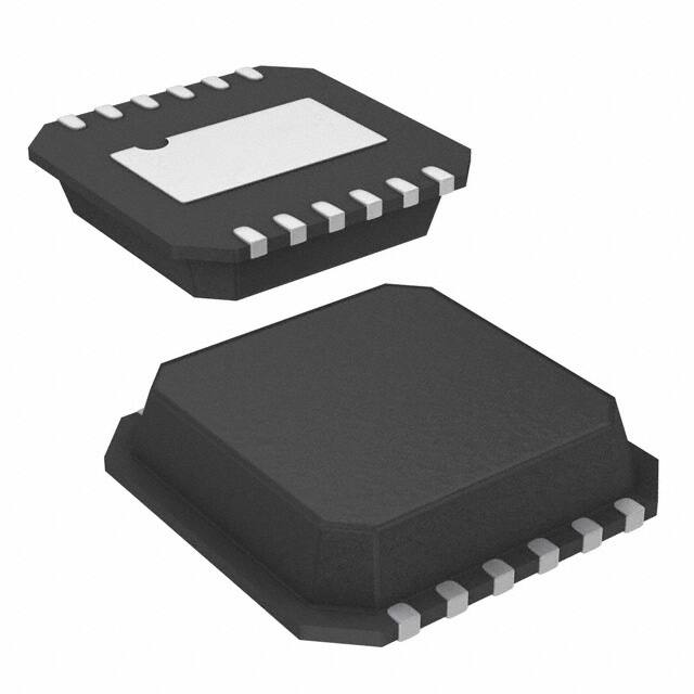
• SOIC, DFN, and TDFN package options
• SOIC, DFN, and TDFN packages compliant with 100V
conductor spacing guidelines per IPC-2221
• Pb-free (RoHS compliant)
• Bootstrap supply max voltage to 114VDC
• On-chip 1W bootstrap diode
• Fast propagation times for multi-MHz circuits
• CMOS compatible input thresholds (ISL2110)
• Independent inputs provide flexibility
Applications
• No start-up problems
• Telecom half-bridge DC/DC converters
• Telecom full-bridge DC/DC converters
• Outputs unaffected by supply glitches, HS ringing below
ground or HS slewing at high dv/dt
• Two-switch forward converters
• Low power consumption
• Active-clamp forward converters
• Wide supply voltage range (8V to 14V)
• Class-D audio amplifiers
• Supply undervoltage protection
• 1.6W/1W typical output pull-up/pull-down resistance
+12V
+100V
SECONDARY
CIRCUIT
VDD
HB
DRIVE
HI
PWM
CONTROLLER
LI
CONTROL
HI
HO
HS
DRIVE
LO
ISL2110
ISL2111
VSS
LO
REFERENCE
AND
ISOLATION
FIGURE 1. APPLICATION BLOCK DIAGRAM
FN6295 Rev.7.00
Mar 16, 2017
Page 1 of 15
�ISL2110, ISL2111
Functional Block Diagram
HB
VDD
UNDER
VOLTAGE
HO
LEVEL SHIFT
DRIVER
HS
HI
ISL2111
ISL2111
UNDER
VOLTAGE
LO
DRIVER
LI
VSS
EPAD (DFN Package Only)
*EPAD = Exposed Pad. The EPAD is electrically isolated from all other pins. For best
thermal performance, connect the EPAD to the PCB power ground plane.
FIGURE 2. FUNCTIONAL BLOCK DIAGRAM
FN6295 Rev.7.00
Mar 16, 2017
Page 2 of 15
�ISL2110, ISL2111
Application Diagrams
+48V
+12V
SECONDARY
CIRCUIT
ISL2110
ISL2111
PWM
ISOLATION
FIGURE 3. TWO-SWITCH FORWARD CONVERTER
+48V
SECONDARY
CIRCUIT
+12V
PWM
ISL2110
ISL2111
ISOLATION
FIGURE 4. FORWARD CONVERTER WITH AN ACTIVE-CLAMP
Ordering Information
PART NUMBER
(Notes 3, 4)
PART
MARKING
TEMP
RANGE
(°C)
PACKAGE
(RoHS COMPLIANT)
PKG.
DWG. #
ISL2110ABZ (Note 1)
2110 ABZ
-40 to +125
8 Ld SOIC
M8.15
ISL2110AR4Z (Note 2)
211 0AR4Z
-40 to +125
12 Ld 4x4 DFN
L12.4x4A
ISL2111ABZ (Note 1)
2111 ABZ
-40 to +125
8 Ld SOIC
M8.15
ISL2111AR4Z (Note 2)
211 1AR4Z
-40 to +125
12 Ld 4x4 DFN
L12.4x4A
ISL2111ARTZ (Note 2)
211 1ARTZ
-40 to +125
10 Ld 4x4 TDFN
L10.4x4
ISL2111BR4Z (Note 2)
211 1BR4Z
-40 to +125
8 Ld 4x4 DFN
L8.4x4
NOTES:
1. Add “-T” for 2.5k unit tape and reel options. Refer to TB347 for details on reel specifications.
2. Add “-T” suffix for 6k unit tape and reel options. Refer to TB347 for details on reel specifications.
3. These Intersil Pb-free plastic packaged products employ special Pb-free material sets, molding compounds/die attach materials, and 100% matte
tin plate plus anneal (e3 termination finish, which is RoHS compliant and compatible with both SnPb and Pb-free soldering operations). Intersil Pbfree products are MSL classified at Pb-free peak reflow temperatures that meet or exceed the Pb-free requirements of IPC/JEDEC J STD-020.
4. For Moisture Sensitivity Level (MSL), please see device information page for ISL2110, ISL2111. For more information on MSL, see Tech Brief TB363.
FN6295 Rev.7.00
Mar 16, 2017
Page 3 of 15
�ISL2110, ISL2111
Pin Configurations
ISL2111ARTZ
(10 LD 4x4 TDFN)
ISL2110AR4Z, ISL2111AR4Z
(12 LD 4x4 DFN)
TOP VIEW
TOP VIEW
VDD
1
10 LO
VDD
1
12 LO
HB
2
9 VSS
NC
2
11 VSS
HO
3
8 LI
NC
3
HS
4
7 HI
HB
4
NC
5
6 NC
HO
5
8
LI
HS
6
7
HI
EPAD*
10 NC
9
NC
*EPAD = EXPOSED PAD
ISL2110ABZ, ISL2111ABZ
(8 LD SOIC)
ISL2111BR4Z
(8 LD 4x4 DFN)
TOP VIEW
TOP VIEW
VDD
1
8
LO
HB
2
7
VSS
HO
3
6
LI
4
5
HI
HS
VDD
1
8
LO
HB
2
7
VSS
HO
3
6
LI
5
HI
HS
4
EPAD*
*EPAD = EXPOSED PAD
Pin Descriptions
SYMBOL
VDD
DESCRIPTION
Positive supply to lower gate driver. Bypass this pin to VSS.
HB
High-side bootstrap supply. External bootstrap capacitor is required. Connect positive side of bootstrap capacitor to this pin. Bootstrap
diode is on-chip.
HO
High-side output. Connect to gate of high-side power MOSFET.
HS
High-side source connection. Connect to source of high-side power MOSFET. Connect negative side of bootstrap capacitor to this pin.
HI
High-side input
LI
Low-side input
VSS
Chip negative supply, which will generally be ground.
LO
Low-side output. Connect to gate of low-side power MOSFET.
NC
No connect
EPAD
Exposed pad. Connect to ground or float. The EPAD is electrically isolated from all other pins.
FN6295 Rev.7.00
Mar 16, 2017
Page 4 of 15
�ISL2110, ISL2111
Absolute Maximum Ratings
Thermal Information
Supply Voltage, VDD, VHB - VHS (Notes 5, 6) . . . . . . . . . . . . . . . 0.3V to 18V
LI and HI Voltages (Note 6) . . . . . . . . . . . . . . . . . . . . . . . -0.3V to VDD + 0.3V
Voltage on LO (Note 6) . . . . . . . . . . . . . . . . . . . . . . . . . . . -0.3V to VDD + 0.3V
Voltage on HO (Note 6) . . . . . . . . . . . . . . . . . . . . . .VHS - 0.3V to VHB + 0.3V
Voltage on HS (Continuous) (Note 6) . . . . . . . . . . . . . . . . . . . . . -1V to 110V
Voltage on HB (Note 6). . . . . . . . . . . . . . . . . . . . . . . . . . . . . . . . . . . . . . . 118V
Average Current in VDD to HB Diode . . . . . . . . . . . . . . . . . . . . . . . . . 100mA
Thermal Resistance (Typical)
JA (°C/W) JC (°C/W)
8 Ld SOIC (Notes 7, 10) . . . . . . . . . . . . . . . .
95
46
10 Ld TDFN (Notes 8, 9) . . . . . . . . . . . . . . .
40
2.5
12 Ld DFN (Notes 8, 9) . . . . . . . . . . . . . . . .
39
2.5
8 Ld DFN (Notes 8, 9). . . . . . . . . . . . . . . . . .
40
4.0
Max Power Dissipation at +25°C in Free Air
8 Ld SOIC (Notes 7, 10) . . . . . . . . . . . . . . . . . . . . . . . . . . . . . . . . . . . . . . 1.3W
10 Ld TDFN (Notes 8, 9) . . . . . . . . . . . . . . . . . . . . . . . . . . . . . . . . . . . . . 3.0W
12 Ld DFN (Notes 8, 9) . . . . . . . . . . . . . . . . . . . . . . . . . . . . . . . . . . . . . . 3.1W
8 Ld DFN (Notes 8, 9) . . . . . . . . . . . . . . . . . . . . . . . . . . . . . . . . . . . . . . 3.1W
Storage Temperature Range. . . . . . . . . . . . . . . . . . . . . . . .-65°C to +150°C
Junction Temperature Range . . . . . . . . . . . . . . . . . . . . . . .-55°C to +150°C
Pb-Free Reflow Profile . . . . . . . . . . . . . . . . . . . . . . . . . . . . . . . . . . see TB493
Maximum Recommended Operating
Conditions
Supply Voltage, VDD . . . . . . . . . . . . . . . . . . . . . . . . . . . . . . . . . . . . . 8V to 14V
Voltage on HS . . . . . . . . . . . . . . . . . . . . . . . . . . . . . . . . . . . . . . . . -1V to 100V
Voltage on HS . . . . . . . . . . . . . . . . . . . . . .(Repetitive Transient) -5V to 105V
Voltage on HB . . . . . . . . . . .VHS + 7V to VHS + 14V and VDD - 1V to VDD + 100V
HS Slew Rate. . . . . . . . . . . . . . . . . . . . . . . . . . . . . . . . . . . . . . . . . . . .


 工商网监
湘ICP备2023018690号
工商网监
湘ICP备2023018690号
