IGNS
NOT RECOMMENDED FOR NEW DES
NT
EME
LAC
REP
NO RECOMMENDED
ter at
contact our Technical Support Cen
/tsc
com
rsil.
.inte
www
or
1-888-INTERSIL
ISL28617
DATASHEET
FN6562
Rev 3.00
May 27, 2015
40V Precision Instrumentation Amplifier with Differential ADC Driver
Features
The ISL28617 is a high performance, differential input,
differential output instrumentation amplifier designed for
precision analog-to-digital applications. It can operate over a
supply range of 8V (±4V) to 40V (±20V) and features a
differential input voltage range up to ±34V. The output stage
has rail-to-rail output drive capability optimized for differential
ADC driver applications. Its versatility and small package
makes it suitable for a variety of general purpose applications.
Additional features not found in other instrumentation
amplifiers enable high levels of DC precision and excellent AC
performance.
• Rail-to-rail differential output ADC driver
• High voltage interface to low voltage circuits
• Wide operating voltage range . . . . . . . . . . . . . . . ±4V to ±20V
• Low input offset . . . . . . . . . . . . . . . . . . . . . . . . . . . . . . . . . 30µV
• Excellent CMRR and PSRR . . . . . . . . . . . . . . . . . . . . . . . 120dB
• Closed loop -3dB BW . . .0.3MHz (AV = 1k) to 5MHz (AV = 0.1)
• Operating temperature range. . . . . . . . . . . .-40°C to +125°C
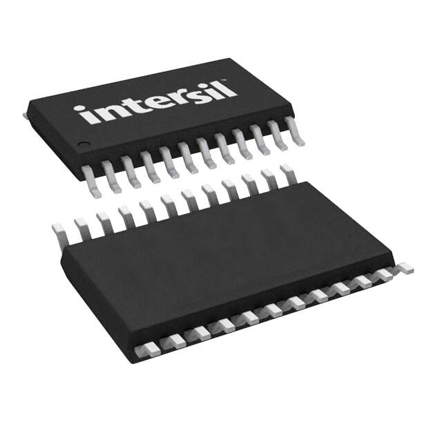
• Package . . . . . . . . . . . . . . . . . . . . . . . . . . . . . . . . 24 Ld TSSOP
The gain of the ISL28617 can be programmed from 0.1 to
10,000 via two external resistors, RIN and RFB. The gain
accuracy is determined by the matching of RIN and RFB. The
gain resistors have Kelvin sensing, which removes gain error
due to PC trace resistance. The input and output stages have
individual power supply pins, which enable input signals riding
on a high common mode voltage to be level shifted to a low
voltage device, such as an A/D converter. The rail-to-rail output
stage can be powered from the same supplies as the ADC,
which preserves the ADC maximum input dynamic range and
eliminates ADC input overdrive.
Applications
• Precision test and measurement
• High voltage industrial process control
• Signal conditioning amplifier for remote powered sensors
• Weigh scales
• ECG and biomedical sense amplifiers
140
AV = 1000
120
Related Literature
AV = 100
CMRR (dB)
100
• AN1753, “ISL28617VYXXEV1Z User’s Guide” Evaluation
board with bulk metal foil resistors for high precision.
• AN1748, “ISL28617SMXXEV1Z User’s Guide” Evaluation
board with standard resistors for low cost, medium
precision.
AV = 10
80
60
AV = 1
40
20
AV = 0.1
0
1
10
100
1k
10k
100k
1M
FREQUENCY (Hz)
FIGURE 1. CMRR RF = 121k
FULL BRIDGE STRAIN GAUGE AMPLIFIER AND DIFFERENTIAL ADC DRIVER
+5V
TO
+20V
RIN
-RIN
-RIN SENSE
BRIDGE
EXCITATION
-5V
TO
-20V
IN+
VCC
+RIN
+RIN SENSE
RFB
VCO
+VFB
ISL28617
+RFB
+RFB SENSE
-RFB
SENSE GND
-RFB
V
EE
IN-
VEO
VCMO
R
+VOUT
VDD
A-D
CONVERTER
+IN
C
-VOUT
-VFB
ISL26132
-IN
R
VREF GND
+5V
VREF
ISL21090
AV = RFB/RIN RANGE FROM 0.1 TO 10,000
FIGURE 2. BASIC APPLICATION CIRCUIT
FN6562 Rev 3.00
May 27, 2015
Page 1 of 20
�ISL28617
Pin Descriptions
ISL28617
(24 LD TSSOP)
TOP VIEW
PIN
NAME
PIN NUMBER
NC
1
DESCRIPTION
NC 1
24 IN+
DNC 2
23 IN-
DNC
2, 3, 22
DNC 3
22 DNC
+RFB
4
Feedback Resistor, RFB+ pin
+RFB 4
21 +RIN
+RFB SENSE
5
+RFB, Positive Sense pin connects to the
resistor RFB+ terminal to form the RFB+
Kelvin connection.
-RFB SENSE
6
-RFB, Negative Sense pin connects to the
resistor RFB- terminal to form the RFBKelvin connection.
+RFB SENSE 5
20 +RIN SENSE
-RFB SENSE 6
19 -RIN SENSE
-RFB 7
18 -RIN
GND 8
17 VCMO
VCC 9
16 VEE
VCO 10
15 VEO
+VFB 11
14 -VFB
+VOUT 12
13 -VOUT
No Internal Connection
For internal use; Do Not Connect.
-RFB
7
Feedback Resistor, Negative Terminal.
GND
8
Ground Pin is capacitively coupled to the
internal ESD circuit and should be
connected to power supply common or
signal GND.
VCC
9
Positive Supply for Input Stage and
Feedback Amp.
VCO
10
Positive Supply for Output Stage.
+VFB
11
Positive Output Feedback
+VOUT
12
Positive Output
-VOUT
13
Negative Output
-VFB
14
Negative Output Feedback
VEO
15
Negative Supply for Output Stage.
VEE
16
Negative Supply for Input Stage and
Feedback Amp.
VCMO
17
Output Common Mode Reference input.
-RIN
18
Input Resistor, Negative Terminal.
-RIN SENSE
19
-RIN, Negative Sense pin connects to the
resistor RIN- terminal to form the RINKelvin connection.
+RIN SENSE
20
+RIN, Positive Sense pin connects to the
resistor RIN+ terminal to form the RIN+
Kelvin connection.
+RIN
21
Input Resistor, Positive Terminal.
IN-
23
Negative Input
IN+
24
Positive Input
Ordering Information
PART NUMBER
(Notes 1, 2, 3)
ISL28617FVZ
PART
MARKING
28617 FVZ
TEMP RANGE
(°C)
-40 to +125
PACKAGE
(RoHS Compliant)
24 Ld TSSOP
PKG.
DWG. #
M24.173
NOTES:
1. Add “-T*” suffix for tape and reel. Please refer to TB347 for details on reel specifications.
2. These Intersil Pb-free plastic packaged products employ special Pb-free material sets, molding compounds/die attach materials, and 100% matte
tin plate plus anneal (e3 termination finish, which is RoHS compliant and compatible with both SnPb and Pb-free soldering operations). Intersil Pbfree products are MSL classified at Pb-free peak reflow temperatures that meet or exceed the Pb-free requirements of IPC/JEDEC J STD-020.
3. For Moisture Sensitivity Level (MSL), please see device information page for ISL28617. For more information on MSL please see tech brief TB363.
FN6562 Rev 3.00
May 27, 2015
Page 2 of 20
�ISL28617
Simplified Block Diagram
+15V
IN+
IN+
ISL28617
VCC
+RINSENSE
VCO
VCC
+RIN
RIN
-RIN
-RINSENSE
IN-
VEE
+VOUT
IN-
-VOUT
+VFB
+RFBSENSE
+OUT
RL
-OUT
VCMO
VCC
+RFB
RFB
-RFB
-RFBSENSE
-VFB
VEE
VEE
GND
-15V
VEO
GND
FIGURE 3. SIMPLIFIED BLOCK DIAGRAM
FN6562 Rev 3.00
May 27, 2015
Page 3 of 20
�ISL28617
Absolute Maximum Ratings
Thermal Information
Maximum Supply Voltage (VCC to VEE or GND) . . . . . . . . . . . . . . . . . . . . 42V
Maximum Supply Voltage (VCO to VEO or GND) . . . . . . . . . . . . . . . . . . . . 42V
Maximum Voltage (VCO to VCC) . . . . . . . . . . . . . . . . . . . . . . . . . . .+0.5V, -40V
Maximum Voltage (VEO to V-) . . . . . . . . . . . . . . . . . . . . . . . . . . . .-0.5V, +40V
Maximum Differential Input Current . . . . . . . . . . . . . . . . . . . . . . . . . . . ±10mA
Max/Min Input Current for Input Voltage >VCC or 100dB and remove CMRR sensitivity to gain
resistor tolerance.
• Provide a level shift interface from bipolar analog input signal
sources to unipolar and bipolar ADC output terminations.
Functional Description
Figure 32 shows the functional block diagram for the ISL28617.
Input GM Amplifier
The input stage consists of high performance, wide band
amplifiers A1, A2, GM drive transistors Q1, Q2 and input gain
resistor RIN. Current drive for Q1 and Q2 emitters are provided by
matched pair of 100µA current sinks. A unity gain buffer from
each input (IN+, IN-) to the terminals of the input resistor, RIN, is
formed by the connection of the Kelvin resistor sense pins and
drive pins to the terminals of the input resistor, as shown in
Figure 32. In this configuration, the voltage across the input
resistor RIN is equal to the input differential voltage across IN+
and IN-.
The input GM stage operates by creating a current difference in
the collector currents Q1 and Q2 in response to the voltage
difference between the IN+ and IN- pins. When the input voltage
applied to the IN+ and IN- pins is zero, the voltage across the
terminals of the gain resistor RIN, is also zero. Since there is no
current flow through the gain resistor, transistors Q1 and Q2
collector currents I1 and I2 are equal.
Error Amplifier A5, Output Amplifier A6
(Figure 32)
Amplifiers A5 and A6 act together to form a high gain,
differential I/O trans impedance amplifier. Differential current
amplifier A5 sums the differential currents (I1 + I3 and I2 + I4)
from the input and feedback GM amplifiers. From that
summation, a differential error voltage is sent to A6, which
generates the rail-to-rail differential output drive to the +VOUT and
-VOUT pins.
The external connection of the output pins to the feedback
amplifier closes a servo loop where a change in the differential
input voltage is converted into differential current imbalances at
I1 and I2 (Equations 1 and 2) at the summing node inputs to A5.
Current I1 sums with current I3 from the feedback stage and I2
sums with I4. A5 senses the difference between current pairs I1,
I3 and I2, I4. A difference voltage is generated, amplified and fed
back to the feedback amplifier, which creates correction currents
at I3 and I4 to match the currents at I1 and I2 (Equations 3 and 4).
Therefore, at equilibrium:
(EQ. 5)
I 1 = I 3 and I 2 = I 4
Combining Equations 1 and 3, (and their complements I2 and I4)
and solving for VOUT as a function of VIN, RIN and RFB, yields
Equation 6:
V OUT = V IN R FB R IN
Where V
= +V
– -V
OUT
OUT
(EQ. 6)
OUT and V IN = IN+ – IN-
Equation 6 can be rearranged to form the gain, see Equation 7:
Gain = V OUT V IN = R FB R IN
(EQ. 7)
Which is general form of the gain equation for the ISL28617.
FN6562 Rev 3.00
May 27, 2015
Page 13 of 20
�ISL28617
Designing with the ISL28617
Setting the Input Gain Resistor RIN
(Figures 32, 33)
To complete a working design, the following procedure is
recommended:
The input gain resistor RIN is scaled to the feedback resistor
according to the gain shown by Equation 9:
1. Define the output voltage swing
3. Set the input gain resistor value, RIN
4. Set the VCO, VEO power supply voltages
5. Set the VCC and VEE supply voltages
The gain of the instrumentation amplifier is set by the resistor
ratio RFB/RIN (Equation 7) and the maximum output swing is set
by the absolute value of the feedback resistor RFB (Equation 8).
VCO and VEO supply power to the rail-to-rail output stage and
define the maximum output voltage swing at the ±VOUT
differential output pins. Power supply pins VCC and VEE power the
feedback amplifiers, which require an additional ±3V beyond the
VCO and VEO voltages to maintain linear operation of the
feedback GM stage.
Setting the Feedback Gain Resistor RFB
(Figures 32, 33)
Resistor RFB defines the maximum differential voltage at output
terminals +VOUT to -VOUT. External resistor RFB and the differential
100µA current sources define the maximum dynamic range of
the feedback stage, which defines the maximum differential
output swing of the output stage. Overload circuitry allows
>100µA to flow through RFB to maintain feedback, but linearity is
degraded. Therefore, it is a good practice to keep the maximum
linear dynamic range to within ±80% of the maximum I*R across
the resistor.
The input GM stage uses the same differential current source
arrangement as the feedback stage. Therefore, the amount of
overdrive margin (50%, 80%) included in the calculation for RFB
is also included in the calculation for RIN.
Input Stage Overdrive Considerations
(Figure 34)
There are a few cases where the input stage can be overdriven,
which must be considered in the application. An input signal that
exceeds the maximum dynamic range of the gain resistor RIN,
calculated previously, can cause the ESD diodes to conduct.
When this occurs, a low impedance path from the inputs to the
input gain resistor RIN will result in signal distortion.
High-speed input signals that remain within the maximum
dynamic range of the input stage can cause distortion if the input
slew rate exceeds the input stage slew rate (~4V/µs). When the
input slews at a faster rate than the GM stage can follow, the
voltage difference appears across the input ESD diodes from
each input and resistor RIN. When the voltage difference is large
enough to cause the diodes to conduct, the input terminals are
shunted to RIN through the 500Ωinput protection resistors,
causing distortion during the rise and fall times of the transient
pulse. The distortion will last until the resistor voltage catches up
to the input voltage.
(EQ. 8)
V OUT DIFF = ±80 A R FB
In cases where large pulse overshoot is expected, the maximum
current in Equation 8 could be reduced to 50% for additional
margin (see “AC Performance Considerations” on page 16). The
penalty for increasing the feedback resistor value is higher DC
offset voltage and noise.
Output voltages that exceed the maximum dynamic range of the
feedback amplifier can degrade phase margin and cause
instability. The plot in Figure 33 shows the maximum differential
output voltage swing vs resistor value for RFB and RIN using the
80% and 50% current source levels.
DYNAMIC VOLTAGE RANGE (±V)
(EQ. 9)
R IN = R FB Gain
2. Set the feedback resistor value, RFB
IN-
500Ω
VCC
IN+
500Ω
+
A1
-
Q1
RIN
Q2
+
A2
ESD
PROTECTION
ESD
PROTECTION
100µA
100µA
35
VEE
30
FIGURE 34. INPUT STAGE ESD PROTECTION DIODES
25
VOUT (V) AT 80%
20
Setting the Power Supply Voltages
15
10
VOUT (V) AT 50%
5
0
0
50
100
150
200
250
300
RFB, RIN VALUE (kΩ)
FIGURE 33. RFB, RIN vs DYNAMIC RANGE
FN6562 Rev 3.00
May 27, 2015
350
400
The ISL28617 power supplies are partitioned so that the input stage
and feedback stages are powered from a separate pair of supply
pins (VCC, VEE) than the differential output stage (VCO, VEO). This
partitioning provides the user with the ability to adapt the ISL28617
to a wide variety of input signal power sources that would not be
possible if the supplies were strapped together internally (VCC = VCO
and VEE = VEO). However, powering the input and output supplies
from unequal supplies has restrictions that are described in the next
section.
Page 14 of 20
�ISL28617
Powering the Input and Feedback Stages
(VCC, VEE)
The input pins IN+, IN- cannot swing rail-to-rail, but have a
maximum input voltage range given by Equation 10:
V EE + 3V V CMIR IN + V IN V CC – 3V
(EQ. 10)
Where VIN = maximum differential voltage IN+ to IN-
This requires the sum of the common mode input voltage and
the differential input voltage to remain within 3V of either the VCC
or VEE rail, otherwise distortion will result.
The feedback pins VFB+ and VFB- have the same input common
mode voltage constraint as the input pins IN+ and IN-. The
maximum input voltage range of the feedback pins is given by
Equation 11:
V EE + 3V V CMIR FB V CC – 3V
(EQ. 11)
Where V CMIR FB = +V OUT – -V OUT + V CMO
To maintain stability, it is critical to respect the ±3V requirement
in Equation 11.
Powering the Rail-to-rail Output Stage
(VCO, VEO)
Power Supply Voltages by Application
The ISL28617 can be adapted to a wide variety of
instrumentation amplifier applications where the signal source is
powered from supply voltages that are different from the supply
voltages powering downstream circuits. The following examples
are included as a guide to the proper connection and voltages
applied to the supply pins VCC, VEE, VCO and VEO.
There are a common set of requirements across all power
applications:
1. A common ground connection from the input supplies, (VCC,
VEE) to the output supplies (VCO, VEO) is required for all
powering options.
2. The signal input pins IN+ and IN- cannot float and must have
a DC return path to ground.
3. The input and output supplies cannot both be operated in
single supply mode due to the 3V feedback amplifier
common mode headroom requirement in Equation 11.
The following are typical power examples:
EXAMPLE 1: BIPOLAR INPUT TO SINGLE SUPPLY
OUTPUT
The ISL28617 is configured as a 5V ADC driver in a high-gain
sensor bridge amplifier powered from a ±10V excitation source.
The sensor signal output is at a much lower voltage level. In this
application, the ISL28617 must extract the low-level bipolar
sensor signal and shift the level to the 0V to +5V differential
rail-to-rail signal needed by the ADC. The following powering
option is recommended:
The output stage (A6) is of rail-to-rail design and is powered by the
VCO and VEO pins. The differential output pins +VOUT and -VOUT
connect to the VFB+ and VFB- pins to close the output feedback
loop. The feedback stage is powered from VCC and VEE pins. The
VFB+ and VFB- have a common mode input range 3V below the VCC
rail and 3V above the and VEE rail. If the output voltage exceeds the
feedback common mode input voltage, loop instability will result.
Therefore, the voltages at the ±VOUT pins should always be 3V
away from either rail, as shown in Equation 12:
• VCO = +5V, VEO = GND
V EE + 3V V OUT V CC – 3V
• VCMO = +2.5V
Where V OUT = +V OUT or -V OUT
(EQ. 12)
Rail-to-rail Differential ADC Driver
The differential output stage of ISL28617 is designed to drive the
differential input stage of an ADC. In this configuration, the VCO
and VEO power supply pins connect directly to the ADC power
supply pins. This output swing arrangement is ideal for driving
rail-to-rail ADC drive without the possibility of overdriving the ADC
input.
The output stage is capable of rail-to-rail operation when VCO and
VEO are powered from a single supply or from split supplies. It
has a single supply voltage range (VCO) from 3V to 15V (with VEO
at GND) and a ±1.5V to ±15V split supply voltage range. Under all
power supply conditions, VCC must be greater than VCO by 3V and
VEE must be less than VEO by 3V to maintain the rail-to-rail output
drive capability.
The VCMO pin is an input to a very low bias current terminal and
sets the output common mode reference voltage when driving a
differential input ADC, such that the output would have a ± input
signal span centered around an external DC reference voltage
applied to the VCMO pin.
FN6562 Rev 3.00
May 27, 2015
• VCC = +10V, VEE = -10V
• VCC and VEE power supply common connects to GND
EXAMPLE 2: HIGH VOLTAGE BIPOLAR I/O BUFFER
The ISL28617 is configured as a high impedance buffer
instrumentation amplifier in a ±15V industrial sensor application. In
this application, the ISL28617 must extract and amplify the high
impedance sensor signal and send it downstream to a differential
ADC operating from ±15V supplies. The following powering options
are recommended:
1. Input and output supplies are strapped to the same supplies and
rail-to-rail input to the ADC is not required.
-
VCC = VCO = +15V
VEE = VEO = -15V
VCMO = GND
VCC, VEE power supply common connects to GND
and VOUT = ±12V
2. ±15V Rail-to-rail output is required, then:
-
VCC = +18V, VEE = -18V
VCO = +15V, VEO = -15V
VCMO = GND
VCC and VEE power supply common connects to GND
Page 15 of 20
�ISL28617
The VCO and VEO power supply pins connect to the ADC (±15V) power
supply pins. Rail-to-rail output swing requires that VCC = VCO +3V and
VEE = VEO -3V, or ±18V.
EXAMPLE 3: GAINS LESS THAN 1
The ISL28617 is configured to a gain of 0.2V/V driving a
rail-to-rail 3V ADC. In this application, the maximum input
dynamic range is ±15V.
- VCC = +18V, VEE = -18V
- VCO = +3V, VEO = GND
- VCMO = +1.5V
- VCC, VEE power supply common connects to GND
In this attenuator configuration, the input signal range is ±15V,
which requires an additional ±3V of input overhead from the
input supplies. Thus, VCC and VEE = ±18V.
AC Performance Considerations
The ISL28617 closed loop frequency response is formed by the
feedback GM amplifier and gain resistor RFB and has the
characteristics of a current feedback amplifier. Therefore, the
-3dB gain does not significantly decrease at high gains as is the
case with the constant gain-bandwidth response of the classic
voltage feedback amplifier.
There are four behaviors of current feedback amplifiers that
must be considered:
• Frequency response increases with decreasing values of RFB.
A comparison of the G = 100, -3db response (Figures 19, 20)
RFB at 30.1kΩvs 121kΩshows almost a 4x decrease from
2MHz to 0.5MHz.
• Gain peaking tends to increase with decreasing values of RFB.
• Wide band applications at gains less than 1 (Figures 19, 20)
can have high gain peaking resulting in high levels of
overshoot with pulsed input signals.
• Parasitic capacitance at the feedback resistor terminals
(+RFB, -RFB) and the Kelvin sense terminals (+RFBSENSE,
-RFBSENSE) will result in increasing levels of peaking and
transient response overshoot.
To minimize peaking external PC parasitic capacitance should be
minimized as much as possible. The ISL28617 is designed to be
stable with PC board parasitic capacitance up to 20pF and
feedback resistor values down to 30.1kΩ. At gains less than 1,
the maximum parasitic capacitance may have to be limited
further to avoid additional compensation.
Uncorrected gain peaking and high overshoot in the feedback
stage can cause loss of feedback loop stability if the transient
causes the feedback voltage to exceed the common mode input
range of the feedback amplifier or the maximum linear range of
the feedback resistor RFB. Corrective actions include increasing
the size of the feedback resistor (see Figure 33) and rescaling
the input gain resistor RIN, or adding input frequency
compensation described in the next section.
The penalty of increasing the RFB (and RIN rescaling) is increased
noise, so this is generally not the corrective action of choice.
FN6562 Rev 3.00
May 27, 2015
AC Compensation Techniques
The input compensation with a low pass filter (Figure 35) can be
an effective way to block high frequency signals from the
differential amplifier inputs. It does not change the gain peaking
behavior of the feedback loop, but it does block signals from
creating overdrive instability. This method is useful after other
corrective measures have been implemented and when there is
little control over the input signal frequency content.
R/2
DIFFERENTIAL
INPUT SIGNAL
IN-
500Ω
IN+
500Ω
C
R/2
COMMON
MODE ERROR
TRACE
CAPACITANCE
GND
FIGURE 35. INPUT DIFFERENTIAL LOW PASS FILTER AND
PARASITIC CAPACITANCE
Input Common Mode Rejection
Considerations
The ISL28617 is capable of a very high level (120dB) of CMRR
performance from DC to as high as 1kHz. (Figure 1; CMRR vs
Frequency). This high level of performance over frequency is
made possible by the high common mode input impedance
(80GΩ but requires careful attention to the matching of the
IN+ and IN- external impedances to GND.
A mismatch in the series impedance in conjunction with parasitic
capacitance at the IN+ and IN- terminals (Figure 35) will cause a
common mode amplitude imbalance that will show up as a
differential input signal, rapidly degrading CMRR as the common
mode frequency increases.
Maximum CMRR performance is achieved with attention to
balancing external components and attention to PC layout.
Layout Guidelines
The ISL28617 is a high precision device with wide band AC
performance. Maximizing DC precision requires attention to the
layout of the gain resistors. Achieving good AC response requires
attention to parasitic capacitance at the gain resistor terminals
and CMRR performance over frequency is ensured with
symmetrical component placement and layout of the input
differential signals to the IN+ and IN- terminals.
To ensure the highest DC precision, the location of the gain
resistors and PC trace connections to the Kelvin connections are
most important. Proper Kelvin connections remove trace
resistance errors so that the amplifier gain accuracy and gain
temperature coefficients are determined by the gain resistor
matching tolerance. Interconnect constraints preclude mounting
the gain resistors next to each other, so they should be located on
either side of the ISL28617 and as close to the device as
Page 16 of 20
�ISL28617
possible. The Kelvin connections are formed at the junction of
the sense pins (±RINSENSE, ±RFBSENSE) and the gain resistor
current drive terminals (±RIN, ±RFB) terminals. This junction
should be made at the terminal pads directly under the ends of
each resistor.
Reduced trace lengths that maintain DC accuracy are also
important for minimizing the capacitance that can degrade AC
stability. This is especially true at gains less than 1. Layout
techniques for precision applications using larger size precision
gain resistors at very low gains (G = 0.1V/V) include removing a
section of the underlying PC ground plane directly under the gain
resistor terminals and body.
Layout guidelines for high CMRR include matching trace lengths
and symmetrical component placement on the circuit that
connects the signal source to the IN+ and IN- pins. This ensures
matching of the IN+ and IN- input impedances (Figure 35).
Power Supply Decoupling
Standard power supply decoupling consists of a single 0.1µF
50V ceramic capacitor at the power supply terminals located as
close to the device as possible. In applications where the input
and output supplies are strapped to the same voltage (VEE = VEO,
VCC = VCO) the connection point should be as close to the device
as possible, with a single 0.1µF 50V ceramic capacitor at the
junction. Applications using separate supplies require 0.1µF 50V
ceramic decoupling capacitors at each power supply terminal.
Estimating Amplifier DC and
Noise Performance
The gain resistor ohmic values and ratios are all that is required
to estimate DC offset and noise. The following sections illustrate
methods to calculate DC offset and noise performance. These
estimates are useful for optimizing resistor values for noise and
DC offset.
Equation 15 converts the output offset error range (Equation 13)
to an input referred error range [VOS(RTI)] and enables a
comparison with the DC component of the input signal.
V OS RTI = V OS(I) + V OS(FB) A V + I ERR R FB A V
(EQ. 15)
Similarly, Equation 16 shows the typical DC offset value
(Equation 14) referred to the input.
2
2
2
V OS RTI TYP = √ V OS(I) + V OS(FB) A V + I ERR R FB A V
(EQ. 16)
NOTE: These results are summarized in Table 1.
Calculating Noise Voltage
The calculation of noise spectral density at the output [eN(RTO)]
from all noise sources is given by Equations 17 and 18:
2
2
e N RTO = √ A V e N I + 2 A V i N I 500 +
2
2
2
A V 4kT R IN + 4kT R FB + R FB i N I ERR + e N FB
(EQ. 17)
Then converts the output noise to the input referred value when
evaluating the input signal to noise ratio.
e N RTI = e N RTO A V
(EQ. 18)
Table 2 provides examples of the noise contribution of each
source by circuit gain and output voltage span. In a high-gain
configuration, the input noise is the dominant noise source. In a
low-gain configuration, the noise voltage from the product of the
internal noise current, IN(err) and the feedback resistor, RFB
dominates. The contribution of the internal noise current, IN(err)
increases in proportion to RFB, but the corresponding increase in
output voltage with RFB keeps the ratio of this noise voltage to
output voltage constant.
Calculating DC Offset Voltage
Output offset voltage, like output noise, has several contributors.
Also similar to output noise, the major offset contributor depends
on the gain configuration. In high-gain, VOS(I) dominates, while in
low-gain, offset due to IERR dominates.
The summation of DC offsets to arrive at total DC offset error is
performed in two ways. Equation 13 is a simple addition of the
DC offsets appearing at the output and is useful when defining
the minimum to maximum range of offset that can be expected.
The drawback is that the result defines the corner of the corner
of the error box and not a typical value given that these sources
are uncorrelated.
V OS RTO = A V V OS(I) + V OS(FB) + I ERR R FB
(EQ. 13)
Equation 14 expresses the total DC error as the rms, or square
root of the sum of the squares to provide an estimate of a typical
value.
2
2
2
V OS RTO TYP = √ A V V OS(I) + V OS(FB) + I ERR R FB
(EQ. 14)
FN6562 Rev 3.00
May 27, 2015
Page 17 of 20
�ISL28617
TABLE 1. COMPUTING TYPICAL OUTPUT OFFSET VOLTAGE RANGES
AV
VO(LIN)
RIN
(kΩ)
RFB
(kΩ)
AV x VOS(I)
(µV)
(Note 11)
1
±2.5
30
30
±30
VOS(FB)
(µV)
(Note 11)
±400
TYPICAL
TYPICAL
IERR (5nA) x RFB
VOS(RTO)
VOS(RTI)
VOS(RTO)
VOS(RTI)
(µV)
(µV)
(µV)
(µV)
(µV)
(Equation 13) (Equation 15) (Equation 14) (Equation 16)
(Note 11)
±150
±580
428
1
±10
120
120
±15
±400
±600
100
±2.5
0.3
30
±1500
±400
±150
±2000
±1015
±20
1560
721
15.6
100
±10
1.2
120
±1500
±400
±600
±2500
±25
1669
16.7
RFB x iN(IERR)
(nV/√Hz)
eN(FB)
(nV/√Hz)
eN (RTO)
OUTPUT
REFERRED
NOISE
(nV/√Hz)
NOTE:
11. Chosen for illustration purposes and does not reflect actual device performance.
TABLE 2. 1kHz INPUT NOISE AND THERMAL NOISE CONTRIBUTIONS
eN (RTI)
INPUT
REFERRED
NOISE
(nV/√Hz)
AV
RIN
(kΩ)
RFB
(kΩ)
AV x eN(I)
(nV/√Hz)
2 x AV x iN(I)
x 500
(nV/√Hz)
1
30
30
8.6
0.15
22.3
22.3
78
8.6
86
1
120
120
8.6
0.15
44.6
44.6
300
8.6
307
100
0.3
30
860
15
223
22.3
78
8.6
892
8.9
100
1.2
120
860
15
446
44.6
300
8.6
1015
10.15
AV x √(4kT x RIN) √(4kT x RFB)
(nV/√Hz)
(nV/√Hz)
NOTE:
12. eN and iN values are chosen for illustration purposes and may not reflect actual device performance.
FN6562 Rev 3.00
May 27, 2015
Page 18 of 20
�ISL28617
Revision History
The revision history provided is for informational purposes only and is believed to be accurate, but not warranted. Please go to web to make sure you
have the latest Rev.
DATE
REVISION
CHANGE
May 27, 2015
FN6562.3
The units of the Y axis on Figures 8, 9, 14, 15 changed from "mV" to “µA” and Figure 16 changed from "mA" to
"µA.
On page 15, under EXAMPLE 1, added the following after the first sentence: “The sensor signal output is at a
much lower voltage level”.
November 17, 2014
FN6562.2
Corrected Typo under “Recommended Operating Conditions” on page 4 from “VE+ to VEO”.
Removed Important note (All parameters having Min/Max specifications are guaranteed. Typ values are for
information purposes only. Unless otherwise noted, all tests are at the specified temperature and are pulsed
tests, therefore: TJ = TC = TA) on page 4 as Note 6 covers this.
Updated About Intersil verbiage.
October 17, 2013
FN6562.1
Added a description to the “Related Literature” on page 1.
“Thermal Information” on page 4: Added theta jc (top) = 28C/W.
Added two new graphs for common mode range vs output voltage (Figure 17 and 18).
May 25, 2012
FN6562.0
Initial release.
About Intersil
Intersil Corporation is a leading provider of innovative power management and precision analog solutions. The company's products
address some of the largest markets within the industrial and infrastructure, mobile computing and high-end consumer markets.
For the most updated datasheet, application notes, related documentation and related parts, please see the respective product
information page found at www.intersil.com.
You may report errors or suggestions for improving this datasheet by visiting www.intersil.com/ask.
Reliability reports are also available from our website at www.intersil.com/support
© Copyright Intersil Americas LLC 2012-2015. All Rights Reserved.
All trademarks and registered trademarks are the property of their respective owners.
For additional products, see www.intersil.com/en/products.html
Intersil products are manufactured, assembled and tested utilizing ISO9001 quality systems as noted
in the quality certifications found at www.intersil.com/en/support/qualandreliability.html
Intersil products are sold by description only. Intersil may modify the circuit design and/or specifications of products at any time without notice, provided that such
modification does not, in Intersil's sole judgment, affect the form, fit or function of the product. Accordingly, the reader is cautioned to verify that datasheets are
current before placing orders. Information furnished by Intersil is believed to be accurate and reliable. However, no responsibility is assumed by Intersil or its
subsidiaries for its use; nor for any infringements of patents or other rights of third parties which may result from its use. No license is granted by implication or
otherwise under any patent or patent rights of Intersil or its subsidiaries.
For information regarding Intersil Corporation and its products, see www.intersil.com
FN6562 Rev 3.00
May 27, 2015
Page 19 of 20
�ISL28617
Package Outline Drawing
M24.173
24 LEAD THIN SHRINK SMALL OUTLINE PACKAGE (TSSOP)
Rev 1, 5/10
A
1
3
7.80 ±0.10
SEE DETAIL "X"
13
24
6.40
PIN #1
I.D. MARK
4.40 ±0.10
2
3
0.20 C B A
1
12
0.15 +0.05
-0.06
B
0.65
TOP VIEW
END VIEW
1.00 REF
H
- 0.05
C
0.90 +0.15
-0.10
1.20 MAX
GAUGE
PLANE
SEATING PLANE
0.25 +0.05
-0.06
0.10 M C B A
0.10 C
5
0°-8°
0.05 MIN
0.15 MAX
SIDE VIEW
0.25
0.60± 0.15
DETAIL "X"
(1.45)
NOTES:
1. Dimension does not include mold flash, protrusions or gate burrs.
(5.65)
Mold flash, protrusions or gate burrs shall not exceed 0.15 per side.
2. Dimension does not include interlead flash or protrusion. Interlead
flash or protrusion shall not exceed 0.25 per side.
3. Dimensions are measured at datum plane H.
4. Dimensioning and tolerancing per ASME Y14.5M-1994.
5. Dimension does not include dambar protrusion. Allowable protrusion
shall be 0.08mm total in excess of dimension at maximum material
condition. Minimum space between protrusion and adjacent lead
(0.65 TYP)
(0.35 TYP)
TYPICAL RECOMMENDED LAND PATTERN
is 0.07mm.
6. Dimension in ( ) are for reference only.
7. Conforms to JEDEC MO-153.
FN6562 Rev 3.00
May 27, 2015
Page 20 of 20
�