DATASHEET
ISL54233
FN7918
Rev.1.00
Dec 12, 2018
Wideband Differential 3:1 Multiplexer
The ISL54233 is a single supply differential 3 to 1 multiplexer
that operates from a single supply in the range of 2.7V to 4.6V. It
was designed to multiplex between three different differential
data sources, allowing the multiplexing of USB 2.0 high speed
data signals, UART data signals and digital video through a
common headphone connector in Personal Media Players and
other portable battery powered devices.
The switch channels have low ON capacitance and high
bandwidth (1.6GHz) to pass USB high speed signals (480Mbps)
and digital video signals with minimal edge and phase distortion
and can swing rail-to-rail to pass UART and full-speed USB
signals.
All channels of the multiplexer can be turned OFF (disabled) by
driving the C0 and C1 logic pins to the low state.
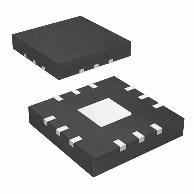
The ISL54233 is available in a tiny 12 Ld 2.2mmx1.4mm
ultra-thin QFN and 12 Ld 3mmx3mm TQFN package. It operates
over a temperature range of -40°C to +85°C.
Features
• High Speed (480Mbps) and Full Speed (12Mbps) Signaling
Capability per USB 2.0 on All Ports
• Digital Video Transmission
• COM Pins Allow Negative Swings to -2V
• All Switches OFF Mode
• Power OFF Protection
• COM Pins Overvoltage Tolerant to 5.5V
• Low ON Capacitance @ 240MHz . . . . . . . . . . . . . . . . . . 2.8pF
• -3dB Frequency. . . . . . . . . . . . . . . . . . . . . . . . . . . . . . . . 1.6GHz
• Single Supply Operation (VDD) . . . . . . . . . . . . . . . . 2.7V to 4.6V
• Available 12 Ld UTQFN and 12 Ld TQFN Packages
• Compliant with USB 2.0 Short Circuit Requirements Without
Additional External Components
• Pb-Free (RoHS Compliant)
Related Literature
Applications
• Technical Brief TB363 “Guidelines for Handling and
Processing Moisture Sensitive Surface Mount Devices
(SMDs)”
• MP4 and Other Personal Media Players
• Mobile Phone/Smart Phone
• Tablets, Readers, GPS and MHL
1
3.3V
VBUS
VDD
C0
0
C1
3DLOGIC
3D+
4MΩ
2D-
DIGITAL
VIDEO
COM -
2D+
COM +
1D-
UART
1D+
GND
USB/DATA JACK
USB
TRANSCEIVER
NORMALIZED GAIN (dB)
µCONTROLLER
-1
-2
-3
-4
RL = 50Ω
VIN = 0dBm, 0.86VDC BIAS
ISL54233
1M
10M
100M
1G
FREQUENCY (Hz)
FIGURE 1. TYPICAL APPLICATION
FN7918 Rev.1.00
Dec 12, 2018
FIGURE 2. BANDWIDTH CHARACTERISTICS CURVE
Page 1 of 19
2G
�ISL54233
Pin Configuration
12 LD 2.2X1.4 UTQFN
TOP VIEW
12 LD 3x3 TQFN
TOP VIEW
VDD
C0
3D-
VDD
C0
12
11
10
12
11
10
LOGIC
CONTROL
1
2
2D+
3
NO
LO
NG
ER
2D-
AV
AI
LA
3D+
BL
E
OR
SU
PP
OR
TE
D
3D-
9
PD
C1
3D+
4MΩ
LOGIC
CONTROL
1
9
C1
4MΩ
8
COM -
7
COM +
2D-
2
8
COM -
2D+
3
7
COM +
4MΩ
4MΩ
4
5
6
1D-
1D+
GND
4
5
6
1D-
1D+
GND
NOTE:
1. ISL54233 switches shown for C1 = Logic “1” and C0 = Logic “0”.
Pin Descriptions
UTQFN
TQFN
NAME
1
1
2
Truth Table
FUNCTION
C1
C0
3D+
USB3/DV Differential Input
0
0
Wired-OR Audio
All switches open
2
2D-
USB2/DV Differential Input
0
1
USB/DV #1
1D- and 1D+ ON
3
3
2D+
USB2/DV Differential Input
1
0
USB/DV #2
2D- and 2D+ ON
4
4
1D-
USB1/DV Differential Input
1
1
USB/DV #3
3D- and 3D+ ON
5
5
1D+
USB1/DV Differential Input
6
6
GND
Ground Connection
7
7
COM+
Data Common Pin
8
8
COM-
Data Common Pin
9
9
C1
Digital Control Input
10
10
C0
Digital Control Input
11
11
VDD
Power Supply
12
12
3D-
USB3/DV Differential Input
-
PAD
PAD
Thermal Pad. Tie to Ground or Float
FN7918 Rev.1.00
Dec 12, 2018
MODE
COMMENTS
C0, C1: Logic “0” when 0.5V or float, Logic “1” when 1.4V with VDD in
range of 2.7V to 3.6V.
Page 2 of 19
�ISL54233
Ordering Information
PART
MARKING
TEMP. RANGE
(°C)
HM
-40 to +85
12 Ld 2.2mmx1.4mm UTQFN (Tape and Reel)
L12.2.2x1.4A
ISL54233IRTZ (Note 4)
4233
-40 to +85
12 Ld 3mmx3mm TQFN
L12.3x3A
ISL54233IRTZ-T (Note 2, 4)
4233
-40 to +85
12 Ld 3mmx3mm TQFN (Tape and Reel)
L12.3x3A
PART NUMBER
ISL54233IRUZ-T (Notes 2, 3) (No
longer available or
supported)
PACKAGE
(Pb-Free)
PKG.
DWG. #
NOTES:
2. Please refer to TB347 for details on reel specifications.
3. These Pb-free plastic packaged products employ special Pb-free material sets; molding compounds/die attach materials and NiPdAu plate - e4
termination finish, which is RoHS compliant and compatible with both SnPb and Pb-free soldering operations. Pb-free products are MSL classified
at Pb-free peak reflow temperatures that meet or exceed the Pb-free requirements of IPC/JEDEC J STD-020.
4. These Pb-free plastic packaged products employ special Pb-free material sets, molding compounds/die attach materials, and 100% matte tin plate
plus anneal (e3 termination finish, which is RoHS compliant and compatible with both SnPb and Pb-free soldering operations). Pb-free products are
MSL classified at Pb-free peak reflow temperatures that meet or exceed the Pb-free requirements of IPC/JEDEC J STD-020.
5. For Moisture Sensitivity Level (MSL), please see device information page for ISL54233. For more information on MSL please see techbrief TB363.
FN7918 Rev.1.00
Dec 12, 2018
Page 3 of 19
�ISL54233
Absolute Maximum Ratings
Thermal Information
VDD to GND . . . . . . . . . . . . . . . . . . . . . . . . . . . . . . . . . . . . . . . . . -0.3V to 5.5V
Input Voltages
1D+, 1D-, 2D+, 2D-, 3D+, 3D- . . . . . . . . . . . . . . . . . . . . . . . . . . -2V to 5.5V
C0, C1 (Note 6) . . . . . . . . . . . . . . . . . . . . . . . . . . . . . . . . . . . . -0.3V to 5.5V
Output Voltages
COM-, COM+ . . . . . . . . . . . . . . . . . . . . . . . . . . . . . . . . . . . . . . . . -2V to 5.5V
Continuous Current (1D-, 1D+, 2D-, 2D+, 3D-, 3D+). . . . . . . . . . . . . . . . . ±40mA
Peak Current (1D-, 1D+, 2D-, 2D+, 3D-, 3D+)
(Pulsed 1ms, 10% Duty Cycle, Max) . . . . . . . . . . . . . . . . . . . . . . ±100mA
ESD Rating:
Human Body Model (Tested per JESD22-A114F) . . . . . . . . . . . . . . . >5kV
Machine Model (Tested per JESD22-A115B) . . . . . . . . . . . . . . . . . >400V
Charged Device Model (Tested per JESD22-C110D) . . . . . . . . . . . . >2kV
Latch-up (Tested per JESD-78B; Class 2, Level A) . . . . . . . . . . . . . . . . . at +85°C
Thermal Resistance (Typical)
JA (°C/W) JC (°C/W)
12 Ld UTQFN Package (Notes 7, 10) . . . . .
155
90
12 Ld TQFN Package (Notes 8, 9) . . . . . . .
58
1.0
Maximum Junction Temperature (Plastic Package) . . . . . . . . . . . +150°C
Maximum Storage Temperature Range. . . . . . . . . . . . . . . . . -65°C to +150°C
Pb-Free Reflow Profile . . . . . . . . . . . . . . . . . . . . . . . . . . . . . . . . . . see TB493
Operating Conditions
Temperature Range . . . . . . . . . . . . . . . . . . . . . . . . . . . . . . . . -40°C to +85°C
Supply Voltage Range . . . . . . . . . . . . . . . . . . . . . . . . . . . . . . . . . 2.7V to 4.6V
CAUTION: Do not operate at or near the maximum ratings listed for extended periods of time. Exposure to such conditions may adversely impact product
reliability and result in failures not covered by warranty.
NOTES:
6. Signals on C1 and C0 exceeding GND by specified amount are clamped. Limit current to maximum current ratings.
7. JA is measured with the component mounted on a high effective thermal conductivity test board in free air. See Tech Brief TB379 for details.
8. JA is measured in free air with the component mounted on a high effective thermal conductivity test board with “direct attach” features. See Tech
Brief TB379.
9. For JC, the “case temp” location is the center of the exposed metal pad on the package underside.
10. For JC, the “case temp” location is taken at the package top center.
Electrical Specifications - 2.7V to 3.6V Supply
Test Conditions: VDD = +3.0V, GND = 0V, VC0H, VC1H = 1.4V, VC0L, VC1L = 0.5V,
(Note 11), Unless Otherwise Specified. Boldface limits apply over the operating temperature range, -40°C to +85°C.
PARAMETER
TEST CONDITIONS
TEMP
(°C)
MIN
(Notes
12, 13)
TYP
MAX
(Notes
12, 13)
UNITS
ANALOG SWITCH CHARACTERISTICS
Analog Signal Range, VANALOG
VDD = 2.7V to 4.6V
Full
-1
-
VDD
V
ON-Resistance, rON
VDD = 2.7V, ICOMx = 17mA, VD+ or VD- = 0V to 400mV
(see Figure 5, Note 15)
25
-
6
8
Ω
rON Matching Between Channels, rON VDD = 2.7V, ICOMx = 17mA, VD+ or VD- = Voltage at max rON,
(Notes 15, 16)
rON Flatness, rFLAT(ON)
VDD = 2.7V, ICOMx = 17mA, VD+ or VD- = 0V to 400mV,
(Notes 14, 15)
ON-Resistance, rON
VDD = 3.3V, ICOMx = 17mA, VD+ or VD- = 3.3V (see Figure 5,
Note 15)
OFF Leakage Current, IXD+(OFF) or
IXD-(OFF), ICOMX(OFF)
VDD = 4.6V, All OFF Mode (C0 = 0.5V, C1 = 0.5V), VCOM- or
VCOM+ = 0.3V, 3.3V, VXD+ or VXD- = 3.3V, 0.3V
ON Leakage Current, IXD+(ON) or
IXD-(ON), ICOMX(ON)
VDD = 4.6V, VXD+ or VXD- = 0.3V, 3.3V, VCOM- or VCOM+ = 0.3V,
3.3V
Full
-
-
10
Ω
25
-
0.07
0.5
Ω
Full
-
-
0.55
Ω
25
-
0.32
0.8
Ω
Full
-
-
1.2
Ω
+25
-
9.5
15
Ω
Full
-
-
20
Ω
25
-15
-
15
nA
Full
-20
-
20
nA
25
-20
-
20
nA
Full
-25
-
25
nA
VDD = 2.7V, RL = 50, CL = 10pF, (see Figure 3)
25
-
125
-
ns
Data Channel to Data Channel Address VDD = 2.7V, RL = 50, CL = 10pF, (see Figure 3)
Transition Time, tTRANS
25
-
125
-
ns
Break-Before-Make Time Delay, tD
VDD = 3.6V, RL = 50, CL = 10pF, (see Figure 4)
25
-
30
-
ns
Skew, (tSKEWOUT - tSKEWIN)
VDD = 3.0V, RL = 45,CL = 10pF,tR = tF = 500ps at 480Mbps,
(Duty Cycle = 50%) (see Figure 8)
25
-
75
-
ps
Total Jitter, tJ
VDD = 3.0V, RL = 50,CL = 10pF,tR = tF = 500ps at 480Mbps
25
-
210
-
ps
DPDT DYNAMIC CHARACTERISTICS
All OFF to ON or ON to All OFF Address
Transition Time, tTRANS
FN7918 Rev.1.00
Dec 12, 2018
Page 4 of 19
�ISL54233
Electrical Specifications - 2.7V to 3.6V Supply
Test Conditions: VDD = +3.0V, GND = 0V, VC0H, VC1H = 1.4V, VC0L, VC1L = 0.5V,
(Note 11), Unless Otherwise Specified. Boldface limits apply over the operating temperature range, -40°C to +85°C. (Continued)
TYP
MAX
(Notes
12, 13)
Rise/Fall Degradation (Propagation
Delay), tPD
VDD = 3.0V, RL = 45,CL = 10pF,see Figure 8)
25
-
250
-
ps
Crosstalk
VDD = 3.0V, RL = 50, f = 240MHz
25
-
-36
-
dB
OFF-Isolation
VDD = 3.0V, RL = 50, f = 240MHz
25
-
-32
-
dB
-3dB Bandwidth
Signal = 0dBm, 0.2VDC offset, RL = 50
25
-
1.6
-
GHz
OFF Capacitance, CXD+OFF, CXD-OFF
f = 1MHz, VDD = 3.0V (see Figure 6)
25
-
3
-
pF
COM ON Capacitance, CCOM-(ON),
CCOM+(ON)
f = 1MHz, VDD = 3.0V (see Figure 6)
25
-
6
-
pF
COM ON Capacitance, CCOM-(ON),
CCOM+(ON)
f = 240MHz, VDD = 3.0V
25
-
2.8
-
pF
Full
2.7
4.6
V
PARAMETER
TEST CONDITIONS
TEMP
(°C)
MIN
(Notes
12, 13)
UNITS
POWER SUPPLY CHARACTERISTICS
Power Supply Range, VDD
Positive Supply Current, IDD
(ALL OFF Mode)
VDD = 3.6V, C1 = GND, C0 = GND
Positive Supply Current, IDD
(USB1 Mode)
VDD = 3.6V, C1 = GND, C0 = VDD
Positive Supply Current, IDD
(USB2 Mode)
VDD = 3.6V, C1 = VDD, C0 = GND
Positive Supply Current, IDD
(USB3 Mode)
VDD = 3.6V, C0 = C1 = VDD
Power OFF COMx Current, ICOMx
VDD = 0V, C0 = C1 = Float, COMx = 5.25V
Power OFF Logic Current, IC0, IC1
VDD = 0V, C0 = C1 = 5.25V
Power OFF D+/D- Current, IXD+, IXD-
VDD = 0V, C0 = C1 = Float, XD- = XD+ = 5.25V
C0, C1 Voltage Low, VC0L, VC1L
VDD = 2.7V to 3.6V
C0, C1 Voltage High, VC0H, VC1H
C0, C1 Input Current, IC0L, IC1L
25
-
6.5
8
µA
Full
-
-
15
µA
25
-
6.5
8
µA
Full
-
-
15
µA
25
-
6.5
8
µA
Full
-
-
15
µA
25
-
6.5
8
µA
Full
-
-
15
µA
25
-
-
1
µA
25
-
11
-
µA
25
-
5
-
µA
Full
-
-
0.5
V
VDD = 2.7V to 3.6V
Full
1.4
-
5.25
V
VDD = 3.6V, C0 = C1 = 0V or Float
Full
-50
6.2
50
nA
C0, C1 Input Current, IC0H, IC1H
VDD = 3.6V, C0 = C1 = 3.6V
Full
-2
1.6
2
µA
C0, C1 Pull-Down Resistor, RCx
VDD = 3.6V, C0 = C1 = 3.6V, Measure current into C0 or C1 pin
and calculate resistance value.
Full
-
4
-
M
DIGITAL INPUT CHARACTERISTICS
NOTES:
11. Vlogic = Input voltage to perform proper function.
12. The algebraic convention, whereby the most negative value is a minimum and the most positive a maximum, is used in this data sheet.
13. Parameters with MIN and/or MAX limits are 100% tested at +25°C, unless otherwise specified. Temperature limits established by characterization
and are not production tested.
14. Flatness is defined as the difference between maximum and minimum value of ON-resistance over the specified analog signal range.
15. Limits established by characterization and are not production tested.
16. rON matching between channels is calculated by subtracting the channel with the highest max rON value from the channel with lowest max rON value,
between 1D+ and 1D- or between 2D+ and 2D- or between 3D+ and 3D-.
FN7918 Rev.1.00
Dec 12, 2018
Page 5 of 19
�ISL54233
Test Circuits and Waveforms
VC0,C1
LOGIC
INPUT
VC0,C1
50%
VINPUT
tOFF
SWITCH
V
INPUT INPUT
VOUT
SWITCH
INPUT
COMx
C0, C1
VOUT
90%
SWITCH
OUTPUT
C
VDD
tr < 20ns
tf < 20ns
90%
LOGIC
INPUT
0V
CL
10pF
RL
50
GND
tON
Logic input waveform is inverted for switches that have the opposite logic
sense.
Repeat test for all switches. CL includes fixture and stray
capacitance.
RL
----------------------V OUT = V
(INPUT) R + r
L
ON
FIGURE 3A. ADDRESS tTRANS MEASUREMENT POINTS
FIGURE 3B. ADDRESS tTRANS TEST CIRCUIT
FIGURE 3. SWITCHING TIMES
VDD
C
3D- OR 3D+
VC0
LOGIC
INPUT
2D- OR 2D+
VINPUT
VC1
VOUT
COMx
1D- OR 1D+
SWITCH
OUTPUT
VOUT
90%
0V
CL
10pF
RL
50
C0, C1
GND
LOGIC
INPUT
tD
Repeat test for all switches. CL includes fixture and stray capacitance.
FIGURE 4B. TEST CIRCUIT
FIGURE 4A. MEASUREMENT POINTS
FIGURE 4. BREAK-BEFORE-MAKE TIME
VDD
C
VDD
rON = V1/17mA
C
CTRL
xD- OR xD+
xD- OR xD+
VD- OR VD+
C0
V1
17mA
C1
0V
VDD
VCx
IMPEDANCE
ANALYZER
COMx
COMx
GND
Repeat test for all switches.
FIGURE 5. rON TEST CIRCUIT
FN7918 Rev.1.00
Dec 12, 2018
VCxL OR
VCxH
GND
Repeat test for all switches.
FIGURE 6. CAPACITANCE TEST CIRCUIT
Page 6 of 19
�ISL54233
Test Circuits and Waveforms (Continued)
VDD
C
CTRL
SIGNAL
GENERATOR
xD-
50Ω
COMx
VCx
0V OR FLOAT
COMx
ANALYZER
50Ω
xD+
N.C.
GND
FIGURE 7. CROSSTALK TEST CIRCUIT
VDD
C
tri
90%
DIN+
DIN-
10%
50%
tskew_i
90%
0V
C0
VDD
C1
15.8Ω
DIN+
50%
COM+
DIN-
15.8Ω
CL
COM-
CL
143Ω
OUT-
10%
50%
tskew_o
50%
90%
45Ω
OUT-
D-
90%
OUT+
OUT+
D+
143Ω
10%
tfi
tro
VDD
45Ω
GND
|tro - tri| Delay Due to Switch for Rising Input and Rising Output Signals
|tfo - tfi| Delay Due to Switch for Falling Input and Falling Output Signals.
tf0
10%
|tskew_0| Change in Skew through the Switch for Output Signals
|tskew_i| Change in Skew through the Switch for Input Signals
FIGURE 8A. MEASUREMENT POINTS
FIGURE 8B. TEST CIRCUIT
FIGURE 8. SKEW TEST
FN7918 Rev.1.00
Dec 12, 2018
Page 7 of 19
�ISL54233
Application Block Diagram
3.3V
µCONTROLLER
100Ω
VDD
3D-
DIGITAL
VIDEO
3D+
C0
LOGIC CONTROL
4MΩ
2D-
C1
COM -
2D+
COM +
1D-
UART
1D+
GND
AUDIO
CODEC
ISL54233
HEAD
PHONE
JACK
ISL54406
Detailed Description
The ISL54233 device consists of dual SP3T (single pole/triple
throw) analog switches. It operates from a single DC power
supply in the range of 2.7V to 4.6V. It was designed to function as
a differential 3 to 1 multiplexer to select between three different
differential data signals. It is offered in tiny UTQFN and TQFN
packages for use in MP3 players, PDAs, cellphones, and other
personal media players.
The device consists of six 6Ω data switches. It was designed to
pass high-speed USB differential data and digital video signals
with minimal edge and phase distortion. It can swing rail-to-rail to
pass UART and full-speed USB signals.
The COM pins can accept signals that swing below ground by as
much as -2V. This allows an audio source to be wired-OR
connected at the COM pins.
The ISL54233 was specifically designed for MP3 players,
personal media players and cellphone applications that need to
combine three differential data channels into a single shared
connector, thereby saving space and component cost. This
functionality is shown in the Typical Application Block Diagram
on page 1.
VBUS
USB/DATA JACK
USB
TRANSCEIVER
These switches can also swing rail-to-rail and pass USB full-speed
(12Mbps) and UART signals with minimal distortion. See
Figure 17 for USB full-speed Eye Pattern taken with the switch in
the signal path.
The maximum normal operating signal range for the USB
switches is from -1V to VDD. The signal voltage at D- and D+
should not be allowed to exceed the VDD voltage rail or go below
ground by more than -1V for normal operation.
Fault Protection and Power-Off Protection
However, in the event that the USB 5.25V VBUS voltage were
shorted to one or both of the COM pins, the ISL54233 has fault
protection circuitry to prevent damage to the ISL54233 part. The
fault circuitry allows the signal pins (COM-, COM+, 1D-, 1D+, 2D-,
2D+, 3D-, 3D+) to be driven up to 5.25V while the VDD supply
voltage is in the range of 0V to 4.6V. This fault condition causes
no stress to the IC.
In addition, when VDD is at 0V (ground) all switches are OFF and
the fault voltage is isolated from the other side of the switch
(Power-Off Protection).
A detailed description of the switches is provided in the following
sections.
When VDD is in the range of 2.7V to 4.6V, the fault voltage will
pass through to the output of an active switch channel.
Note: During the fault condition, normal operation is not
guaranteed until the fault condition is removed.
Data Switches
ISL54233 Operation
The six data switches (1D+, 1D-, 2D+, 2D-, 3D+, 3D-) are 6Ω
bidirectional switches that were specifically designed to pass
high-speed USB differential data signals in the range of 0V to
400mV. The switches have low capacitance and high bandwidth
to pass USB high-speed signals (480Mbps) with minimum edge
and phase distortion to meet USB 2.0 signal quality
specifications. See Figures 15 and 16 for high-speed Eye Pattern
taken with the switch in the signal path.
The discussion that follows will discuss using the ISL54233 in the
“Application Block Diagram” on page 8.
FN7918 Rev.1.00
Dec 12, 2018
Page 8 of 19
�ISL54233
POWER
USB/DV 1 Mode
The power supply connected at VDD (pin 11) provides power to
the ISL54233 part. Its voltage should be kept in the range of
2.7V to 4.6V. In a typical application, VDD will be in the range of
2.7V to 4.3V and will be connected to the battery or LDO of the
MP3 player or cellphone.
If the C1 pin = Logic “0” and C0 pin = Logic “1” the part will go
into USB/DV1 mode. The 1D- and 1D+ switches are ON and the
2D- and 2D+ switches and 3D- and 3D+ will be OFF (high
impedance).
A 0.01µF or 0.1µF decoupling capacitor should be connected
from the VDD pin to ground to filter out any power supply noise
from entering the part. The capacitor should be located as close
to the VDD pin as possible.
If the C1 = Logic “1” and C0 pin = Logic “0” the part will be in the
USB/DV2 mode. The 2D- and 2D+ switches will be ON and the
1D- and 1D+ switches and the 3D- and 3D+ will be OFF (high
impedance).
LOGIC CONTROL
USB/DV 3 Mode
The state of the ISL54233 device is determined by the voltage at
the C1 pin (pin 9) and the C0 pin (pin 10). Refer to the “Truth
Table” on page 2.
If the C1 pin = Logic “1” and C0 pin = Logic “1” the part will be in
the USB/DV3 mode. The 3D- and 3D+ switches are ON, and the
1D- and 1D+ switches and 2D- and 2D+ switches will be OFF
(high impedance).
The C1 pin and C0 pin are internally pulled low through 4M
resistors to ground and can be tri-stated or left floating.
The C1 pin and C0 pin can be driven with a voltage that is higher
than the VDD supply voltage. They can be driven up to 5.25V with
the VDD supply in the range of 2.7V to 4.6V. Driving the logic
higher than the supply rail will cause the logic current to
increase. With VDD = 2.7V and VLOGIC = 5.25V, ILOGIC current is
approximately 5.5µA.
Logic Control Voltage Levels
With VDD in the range of 2.7V to 3.6V the logic levels are: C1,
C0 = Logic “0” (Low) when 0.5V or Floating. C1, C0 = Logic “1”
(High) when 1.4V.
ALL SWITCHES OFF Mode
If the C1 pin = Logic “0” and C0 pin = Logic “0” the part will be in
the ALL SWITCHES OFF mode. In this mode, the 3D- and 3D+
data switches, the 2D- and 2D+ data switches, and the 1D- and
1D+ data switches will be OFF (high impedance).
The COM pins can accommodate signals that swing below
ground by as much as -2V. This allows an audio CODEC to be
connected to the COM pins when the device is in the all off state.
USB/DV 2 Mode
Printed Circuit Board Design for High
Frequency Performance
In 50Ω systems, the ISL54233 has a -3dB bandwidth of 1.6GHz
(see Figure 19).
To achieve this high bandwidth requires careful design and layout
of the PCB board. Signal traces must be designed to minimize
reflections and reduce parasitic resistance, inductance and
capacitance that degrade the frequency response performance.
Figure 9 shows a picture of the engineering board used to
measure the frequency response of the ISL54233 part. The
board was specifically design for taking high frequency
bandwidth measurements. The board was made with special
materials and was carefully layed out using RF board techniques
to maximize it for high frequency operation.
The next section, “Board Layout Guidelines”, will provide a list of
the PCB board requirements needed to get the maximum
bandwidth from the ISL54233 part when tested with a 50
Network Analyzer.
FIGURE 9. RF HIGH FREQUENCY BOARD
FN7918 Rev.1.00
Dec 12, 2018
Page 9 of 19
�ISL54233
BOARD LAYOUT GUIDELINES
• The ISL54233 device must be soldered directly onto the
PCB board. No IC sockets can be used. Their parasitic
impedance will degrade the frequency performance.
• Route all controlled impedance signal lines on the top
(signal) layer with no vias or through holes. Vias or through
holes make it difficult to maintain a controlled impedance
and tend to generate reflections.
• The signal traces (1D+, 1D-, 2D+, 2D-, 3D+, 3D-, COM- and
COM+) must have a controlled (characteristic) impedance of
50Ω±5%Tight control on trace width and dielectric
thickness must be followed to get 50Ωlines. Impedance
tests results for controlled lines should be requested from
the board fabrication house.
• The signal trace lengths should be as short (