DATASHEET
ISL6269B
High-Performance Notebook PWM Controller With Audio-Frequency Clamp
The ISL6269B IC is a Single-phase Synchronous-Buck PWM
controller featuring Intersil's Robust Ripple Regulator R3™
Technology that delivers truly superior dynamic response to
input voltage and output load transients. Integrated MOSFET
drivers and bootstrap diode result in fewer components and
smaller implementation area.
Features
Intersil’s R3™ Technology combines the best features of
fixed-frequency PWM and hysteretic PWM while eliminating
many of their shortcomings. R3™ Technology employs an
innovative modulator that synthesizes an AC ripple voltage
signal VR, analogous to the output inductor ripple current. The
AC signal VR enters a window comparator where the lower
threshold is the error amplifier output VCOMP and the upper
threshold is a programmable voltage reference VW, resulting in
generation of the PWM signal. The voltage reference VW sets
the steady-state PWM frequency. Both edges of the PWM can be
modulated in response to input voltage transients and output
load transients, much faster than conventional fixed-frequency
PWM controllers. Unlike a conventional hysteretic converter, the
ISL6269B has an error amplifier that provides ±1% voltage
regulation at the FB pin.
• Wide input voltage range: +5V to +25V
The ISL6269B has a 1.5ms digital soft-start and can be
started into a pre-biased output voltage. A resistor divider is
used to program the output voltage setpoint. The ISL6269B
can be configured to operate in Continuous Conduction Mode
(CCM) or Diode Emulation Mode (DEM), which improves
light-load efficiency. In CCM the controller always operates as a
synchronous rectifier, however when DEM is enabled, the
low-side MOSFET is permitted to stay off, blocking negative
current flow into the low-side MOSFET from the output
inductor.
FN6280
Rev 3.00
November 17, 2014
• High performance R3™ Technology
• Fast transient response
• ±1% regulation accuracy: -10°C to +100°C and
-40° to +100°C
• Output voltage range: +0.6V to +3.3V
• Wide output load range: 0A to 25A
• Selectable diode emulation mode for increased light load
efficiency
• Programmable PWM frequency: 200kHz to 600kHz
• Pre-biased output start-up capability
• Integrated MOSFET drivers and bootstrap diode
• Internal digital soft-start
• Power-good monitor
• PWM minimum frequency above audible spectrum
• Fault protection
- Undervoltage protection
- Soft crowbar overvoltage protection
- Low-side MOSFET rDS(ON) overcurrent protection
- Over-temperature protection
- Fault identification by PGOOD pull-down resistance
• Pb-free (RoHS compliant)
Applications
• PCI express graphical processing unit
• Auxiliary power rail
• VRM
• Network adapter
FN6280 Rev 3.00
November 17, 2014
Page 1 of 16
�ISL6269B
Ordering Information
PART NUMBER
(Notes 1, 2, 3)
PART
MARKING
TEMP RANGE
(°C)
PACKAGE
(RoHS Compliant)
PKG. DWG. #
ISL6269BCRZ
62 69BCRZ
-10 to +100
16 Ld 4x4 QFN
L16.4x4
ISL6269BIRZ
62 69BIRZ
-40 to +100
16 Ld 4x4 QFN
L16.4x4
NOTES:
1. Add “-T*” suffix for tape and reel. Please refer to TB347 for details on reel specifications.
2. These Intersil Pb-free plastic packaged products employ special Pb-free material sets, molding compounds/die attach materials and 100% matte tin
plate plus anneal (e3 termination finish, which is RoHS compliant and compatible with both SnPb and Pb-free soldering operations). Intersil Pb-free
products are MSL classified at Pb-free peak reflow temperatures that meet or exceed the Pb-free requirements of IPC/JEDEC J STD-020.
3. For Moisture Sensitivity Level (MSL), please see product information page for ISL6269B. For more information on MSL, please see tech brief TB363.
Pin Configuration
FN6280 Rev 3.00
November 17, 2014
PGOOD
PHASE
UG
BOOT
ISL6269B
(16 LD 4x4 QFN)
TOP VIEW
16
15
14
13
12 PVCC
VIN
1
VCC
2
FCCM
3
10 PGND
EN
4
9
11 LG
5
6
7
8
COMP
FB
FSET
VO
GND
ISEN
Page 2 of 16
�ISL6269B
Functional Pin Descriptions
GND (Bottom Pad)
Signal common of the IC. Unless otherwise stated, signals are
referenced to the GND pin, not the PGND pin.
VIN (Pin 1)
The VIN pin measures the converter input voltage which is a
required input to the R3™ PWM modulator. Connect across the
drain of the high-side MOSFET to the GND pin.
VCC (Pin 2)
The VCC pin is the input bias voltage for the IC. Connect +5V from
the VCC pin to the GND pin. Decouple with at least 1µF of a MLCC
capacitor from the VCC pin to the GND pin.
FCCM (Pin 3)
The FCCM pin configures the controller to operate in Forced
Continuous Conduction Mode (FCCM) or Diode Emulation Mode
(DEM.) DEM is disabled when the FCCM pin is pulled above the
rising threshold voltage VFCCMTHR, conversely DEM is enabled
when the FCCM pin is pulled below the falling threshold voltage
VFCCMTHF.
EN (Pin 4)
The EN pin is the on/off switch of the IC. The soft-start sequence
begins when the EN pin is pulled above the rising threshold
voltage VENTHR and VVCC is above the power-on reset (POR) rising
threshold voltage VVCC_THR . When the EN pin is pulled below the
falling threshold voltage VENTHF PWM immediately stops.
COMP (Pin 5)
The COMP pin is the output of the control-loop error amplifier.
Compensation components for the control-loop connect across
the COMP and FB pins.
FB (Pin 6)
The FB pin is the inverting input of the control-loop error
amplifier. The converter output voltage regulates to 600mV from
the FB pin to the GND pin. Program the desired output voltage
with a resistor network connected across the VO, FB and GND
pins. Select the resistor values such that FB to GND is 600mV
when the converter output voltage is at the programmed
regulation value.
FSET (Pin 7)
The FSET pin programs the PWM switching frequency. Program
the desired PWM frequency with a resistor and a capacitor
connected across the FSET and GND pins.
VO (Pin 8)
ISEN (Pin 9)
The ISEN pin programs the threshold of the OCP overcurrent fault
protection. Program the desired OCP threshold with a resistor
connected across the ISEN and PHASE pins. The OCP threshold is
programmed to detect the peak current of the output inductor.
The peak current is the sum of the DC and AC components of the
inductor current.
PGND (Pin 10)
The PGND pin conducts the turn-off transient current through the
LG gate driver. The PGND pin must be connected to complete the
pull-down circuit of the LG gate driver. The PGND pin should be
connected to the source of the low-side MOSFET through a low
impedance path, preferably in parallel with the trace connecting
the LG pin to the gate of the low-side MOSFET. The adaptive
shoot-through protection circuit, measures the low-side MOSFET
gate-source voltage from the LG pin to the PGND pin.
LG (Pin 11)
The LG pin is the output of the low-side MOSFET gate driver.
Connect to the gate of the low-side MOSFET.
PVCC (Pin 12)
The PVCC pin is the input voltage bias for the LG low-side
MOSFET gate driver. Connect +5V from the PVCC pin to the PGND
pin. Decouple with at least 1µF of an MLCC capacitor across the
PVCC and PGND pins.
BOOT (Pin 13)
The BOOT pin stores the input voltage for the UG high-side
MOSFET gate driver. Connect an MLCC capacitor across the BOOT
and PHASE pins. The boot capacitor is charged through an
internal boot diode connected from the PVCC pin to the BOOT pin,
each time the PHASE pin drops below PVCC minus the voltage
dropped across the internal boot diode.
UG (Pin 14)
The UG pin is the output of the high-side MOSFET gate driver.
Connect to the gate of the high-side MOSFET.
PHASE (Pin 15)
The PHASE pin detects the voltage polarity of the PHASE node
and is also the current return path for the UG high-side MOSFET
gate driver. Connect the PHASE pin to the node consisting of the
high-side MOSFET source, the low-side MOSFET drain and the
output inductor.
PGOOD (Pin 16)
The PGOOD pin is an open-drain output that indicates when the
converter is able to supply regulated voltage. Connect the PGOOD
pin to +5V through a pull-up resistor.
The VO pin measures the converter output voltage and is used
exclusively as an input to the R3™ PWM modulator. Connect at
the physical location where the best output voltage regulation is
desired.
FN6280 Rev 3.00
November 17, 2014
Page 3 of 16
�ISL6269B
VIN
VO
GND
PACKAGE BOTTOM
PWM FREQUENCY
CONTROL
VCC
VREF
FSET
-
FN6280 Rev 3.00
November 17, 2014
Block Diagram
+
+
VW
gmVIN
EN
-
-
+
R
-
PWM
Q
OVP
S
-
VR
+
+
gmVO
-
VCOMP
+
-
CR
UVP
+
-
+
BOOT
+
EA
FB
DRIVER
-
DIGITAL SOFT-START
PWM CONTROL
POR
COMP
ISEN
OCP
PHASE
SHOOT THROUGH
PROTECTION
PVCC
+
IOC
UG
30Ω
90Ω
60Ω
DRIVER
LG
Page 4 of 16
150°OT
PGOOD
PGND
FCCM
�ISL6269B
Typical Application
ISL6269B
VIN
5V TO 25V
PGOOD
VIN
CIN
RPGOOD
QHIGH_SIDE
5V
PVCC
UG
RVCC
VCC
CPVCC
BOOT
CVCC
CBOOT
GND
VOUT
LOUT
0.6V TO 3.3V
PHASE
COUT
RSEN
FCCM
ISEN
QLOW_SIDE
EN
LG
RCOMP
COMP
PGND
CCOMP1
FB
VO
CCOMP2
RBOTTOM
FN6280 Rev 3.00
November 17, 2014
FSET
RFSET
CFSET
RTOP
Page 5 of 16
�ISL6269B
Absolute Maximum Ratings
Thermal Information
SEN, VIN to GND . . . . . . . . . . . . . . . . . . . . . . . . . . . . . . . . . . . . . -0.3V to +28V
VCC, PGOOD to GND. . . . . . . . . . . . . . . . . . . . . . . . . . . . . . . . . . 0.3V to +7.0V
PVCC to PGND . . . . . . . . . . . . . . . . . . . . . . . . . . . . . . . . . . . . . . -0.3V to +7.0V
GND to PGND . . . . . . . . . . . . . . . . . . . . . . . . . . . . . . . . . . . . . . -0.3V to +0.3V
EN, FCCM . . . . . . . . . . . . . . . . . . . . . . . . . . . . . . . . . -0.3V to GND, VCC +3.3V
VO, FB, COMP, FSET . . . . . . . . . . . . . . . . . . . . . . . . -0.3V to GND, VCC +0.3V
PHASE to GND (DC) . . . . . . . . . . . . . . . . . . . . . . . . . . . . . . . . . . -0.3V to +28V
(
很抱歉,暂时无法提供与“ISL6269BCRZ”相匹配的价格&库存,您可以联系我们找货
免费人工找货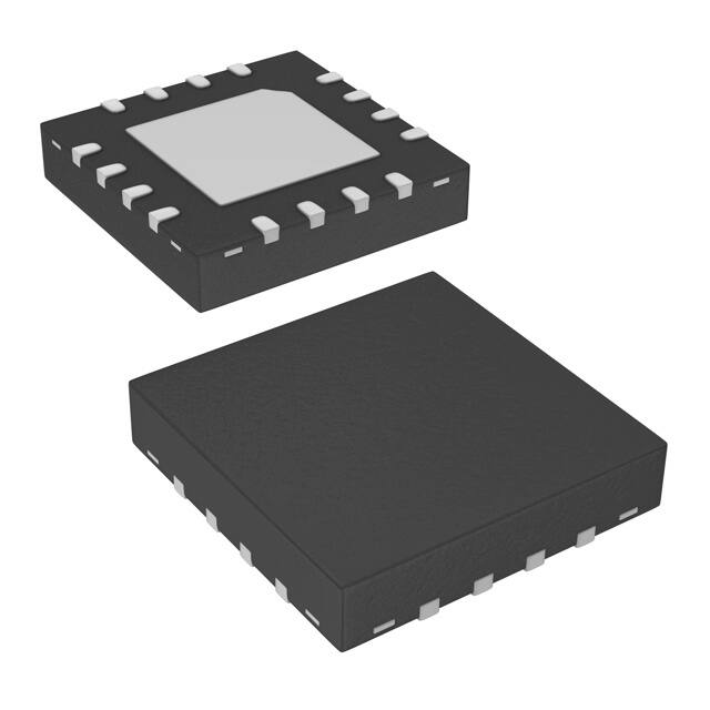


 工商网监
湘ICP备2023018690号
工商网监
湘ICP备2023018690号
