DATASHEET
ISL6567
FN9243
Rev 4.00
August 9, 2011
Multipurpose Two-Phase Buck PWM Controller with Integrated MOSFET Drivers
The ISL6567 two-phase synchronous buck PWM control IC
provides a precision voltage regulation system for point-of-load
and other high-current applications requiring an efficient and
compact implementation. Multi-phase power conversion is a
marked departure from single phase converter configurations
employed to satisfy the increasing current demands of various
electronic circuits. By distributing the power and load current,
implementation of multi-phase converters utilize smaller and
lower cost transistors with fewer input and output capacitors.
These reductions accrue from the higher effective conversion
frequency with higher frequency ripple current resulting from
the phase interleaving inherent to this topology.
Outstanding features of this controller IC include an internal
0.6V reference with a system regulation accuracy of 0.6%, an
optional external reference input, and user-adjustable
switching frequency. Precision regulation is further enhanced
by the available unity-gain differential amplifier targeted at
remote voltage sensing capability, while output regulation is
monitored and its quality is reported via a PGOOD pin. Also
included is an internal shunt regulator with optional external
connection capability which extends the operational input
voltage range. For applications requiring voltage tracking or
sequencing, the ISL6567 offers a host of possibilities,
including coincidental, ratiometric, or offset tracking, as well
as sequential start-ups, user adjustable for a wide range of
applications.
Protection features of this controller IC include overvoltage
and overcurrent protection. Overvoltage results in the
converter turning the lower MOSFETs ON to clamp the rising
output voltage. The ISL6567 uses cost and space-saving
rDS(ON) sensing for channel current balance, dynamic voltage
positioning, and overcurrent protection. Channel current
balancing is automatic and accurate with the integrated
current-balance control system. Overcurrent protection can be
tailored to various application with no need for additional
parts.
Features
• Integrated Two-Phase Power Conversion
- Integrated 4A Drivers for High Efficiency
• Shunt Regulator for Wide Input Power Conversion
- 5V and Higher Bias
- Up to 20V Power-Down-Conversion
• Precision Channel Current Sharing
- Loss-Less Current Sampling - Uses rDS(ON)
• Precision Output Voltage Regulation
- 0.6% System Accuracy Over-Temperature (Commercial
Range)
• 0.6V Internal Reference
• Full Spectrum Voltage Tracking
- Coincidental, Ratiometric, or Offset
• Sequential Start-up Control
• Adjustable Switching Frequency
- 150kHz to 1.5MHz
• Fast Transient Recovery Time
• Unity-Gain Differential Amplifier
- Increased Voltage Sensing Accuracy
• Overcurrent Protection
• Overvoltage Protection
• Start-up into Pre-Charged Output
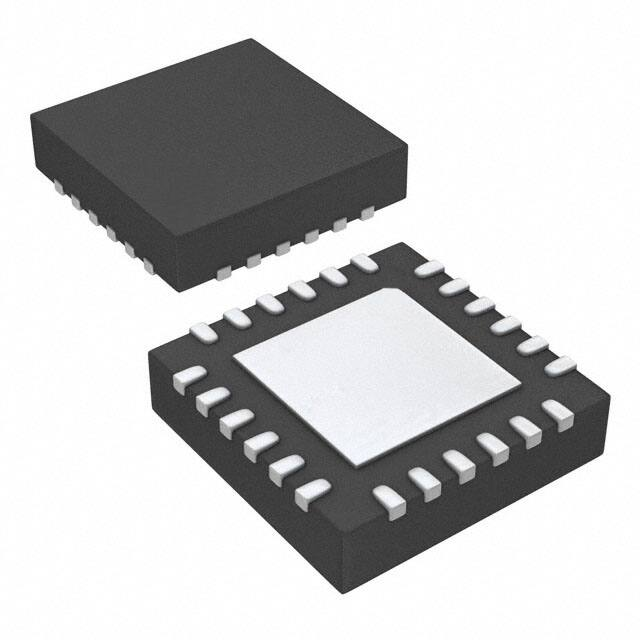
• Small, QFN Package Footprint
• Pb-Free (RoHS Compliant)
Ordering Information
PART NUMBER
(Notes 1, 2, 3)
PART
MARKING
TEMP.
RANGE
(°C)
PACKAGE
(Pb-Free)
PKG.
DWG. #
ISL6567CRZ
65 67CRZ
0 to +70 24 Ld 4x4 QFN L24.4x4C
ISL6567IRZ
65 67IRZ -40 to +85 24 Ld 4x4 QFN L24.4x4C
NOTE:
1. Add “-T*” suffix for tape and reel. Please refer to TB347 for details
on reel specifications.
2. These Intersil Pb-free plastic packaged products employ special
Pb-free material sets, molding compounds/die attach materials,
and 100% matte tin plate plus anneal (e3 termination finish, which
is RoHS compliant and compatible with both SnPb and Pb-free
soldering operations). Intersil Pb-free products are MSL classified
at Pb-free peak reflow temperatures that meet or exceed the Pbfree requirements of IPC/JEDEC J STD-020.
3. For Moisture Sensitivity Level (MSL), please see device information
page for ISL6567. For more information on MSL please see
techbrief TB363.
FN9243 Rev 4.00
August 9, 2011
Page 1 of 26
�ISL6567
Pin Configuration
FN9243 Rev 4.00
August 9, 2011
REFTRK
SS
FS
PGOOD
BOOT1
UGATE1
ISL6567
(24 LD QFN)
TOP VIEW
24
23
22
21
20
19
RGND
1
18 PHASE1
VSEN
2
17 ISEN1
MON
3
VDIFF
4
FB
5
14 LGATE2
COMP
6
13 ISEN2
16 LGATE1
25
GND
7
8
9
10
11
12
VREG
VCC
EN
BOOT2
UGATE2
PHASE2
15 PVCC
Page 2 of 26
�FS
PGOOD
MON
VCC
EN
PVCC
ISL6567
FN9243 Rev 4.00
August 9, 2011
Block Diagram
BOOT1
20µA
300mV +
110%
-
90%
OSCILLATOR
VCC
10µA
UGATE1
POWER-ON
RESET (POR)
10µA
GATE
CONTROL
OVP
PHASE1
COMP
LGATE1
120%
REFTRK
SOFT-START
AND
FAULT LOGIC
REFERENCE
PWM1
GND
CONTROL
LOGIC
EA
FB
BOOT2
PWM2
+
OC
-
VDIFF
VCC
UGATE2
RGND
20µA
X1
VSEN
VREG
VCC
CURRENT
CORRECTION
20µA/1mA
Page 3 of 26
ISEN2
PHASE2
LGATE2
SHUNT LINEAR
REGULATOR
ISEN1
GATE
CONTROL
SS
�ISL6567
Simplified Power System Diagram
VIN
Q1
EN
CHANNEL1
Q2
PGOOD
VOUT
Q3
CHANNEL2
Q4
ISL6567
Typical Application
VIN
LIN
CHFIN1
RSHUNT
CBIN1
CF2
CF1
VCC
VREG
PVCC
BOOT1
CBOOT1
REFTRK
UGATE1
FS
Q1
PHASE1
LOUT1
RFS
ISEN1
SS
RISEN1
CSS
Q2
MON
LGATE1
RPG
BOOT2
PGOOD
CBOOT2
ISL6567
R4
VOUT
CHFIN2
EN
UGATE2
CBIN2
CHFOUT
CBOUT
Q3
R5
PHASE2
ISEN2
C1
LGATE2
R2
RISEN2
C2
GND
RS
LOUT2
COMP
Q4
RP
FB
VDIFF
VSEN
RGND
R1
FN9243 Rev 4.00
August 9, 2011
Page 4 of 26
�ISL6567
Absolute Maximum Ratings
Thermal Information
Supply Voltage, VCC, PVCC . . . . . . . . . . . . . . . . . . . . . . . . . . . -0.3V to +6.5V
Shunt Regulator Voltage, VVREG . . . . . . . . . . . . . . . . . . . . . . . -0.3V to +6.5V
Boot Voltage, VBOOT . . . . . . . . . . . . . . . . . . . . . PGND - 0.3V to PGND + 27V
PHASE Voltage . . . . . . . . . . . . . . . . . . . . . GND - 0.3V (DC) to VBOOT + 0.3V
. . . . . . . . . . . . . . . . GND - 5V (
(EQ. 5)
CHANNEL-CURRENT BALANCE
FIGURE 5. NORMAL SOFT-START WAVEFORMS FOR ISL6567BASED MULTI-PHASE CONVERTER
Another benefit of multi-phase operation is the thermal
advantage gained by distributing the dissipated heat over
multiple devices and greater area. By doing this, the designer
avoids the complexity of driving multiple parallel MOSFETs and
the expense of using expensive heat sinks and exotic magnetic
materials.
Whenever the ISL6567’s power-on reset falling threshold is
tripped, or it is disabled via the EN pin, the SS capacitor is
quickly discharged via an internal pull-down device
(represented as the 1mA, typical, current source).
All things being equal, in order to fully realize the thermal
advantage, it is important that each channel in a multi-phase
converter be controlled to deliver about the same current at
any load level. Intersil’s ISL6567 ensure current balance by
comparing each channel’s current to the average current
delivered by both channels and making appropriate
adjustments to each channel’s pulse width based on the
resultant error. The error signal modifies the pulse width to
correct any unbalance and force the error toward zero.
Should OC protection be tripped while the ISL6567 is
operating in internal-reference mode and the SS pin not be
allowed to fully discharge the SS capacitor, the ISL6567
cannot continue the normal SS cycling.
Conversely, should a channel-to-channel imbalance be desired,
such imbalance can be created by adjusting the individual
channel’s RISEN resistor. Asymmetrical layouts, where one
phase of the converter is naturally carrying more current than
the other, or where one of the two phases is subject to a more
stringent thermal environment limiting its current-carrying
capability, are instances where this adjustment is particularly
useful, helping to cancel out the design-intrinsic thermal or
current imbalances.
As the SS pin’s positive excursion is internally clamped to
about 3.5V, insure that any external pull-up device does not
force more than 3mA into this pin.
OVERCURRENT PROTECTION
The individual channel currents, as sensed via the PHASE pins
and scaled via the ISEN resistors, as well as their combined
average are continuously monitored and compared with an
internal overcurrent (OC) reference. If the combined channel
current average exceeds the reference current, the overcurrent
comparator triggers an overcurrent event. Similarly, an OC
event is also triggered if either channel’s current exceeds the
OC reference for 7 consecutive switching cycles.
SOFT-START
The soft-start function allows the converter to bring up the
output voltage in a controlled fashion, resulting in a linear
ramp-up. As soon as the controller is fully enabled for
operation, the SS pin starts to output a small current which
charges the external capacitor, CSS, connected to this pin. An
internal reference clamp controlled by the potential at the SS
pin releases the reference to the input of the error amplifier
with a 1:1 correspondence for SS potential exceeding 0.7V
FN9243 Rev 4.00
August 9, 2011
Page 11 of 26
�ISL6567
SETTING THE OUTPUT VOLTAGE
OUTPUT CURRENT
EN
GND>
SS
The ISL6567 uses a precision internal reference voltage to set
the output voltage. Based on this internal reference, the output
voltage can thus be set from 0.6V up to a level determined by
the input voltage, the maximum duty cycle, and the conversion
efficiency of the circuit; Equation 7 estimates this maximum
amplitude the output voltage can be regulated to. Obviously,
insure that the input voltage and all the voltages sampled by
the ISL6567 do not exceed the controller’s absolute maximum
limits, or any other limits specified in this document.
ISL6567
EXTERNAL CIRCUIT
VREF
GND>
OUTPUT VOLTAGE
FIGURE 6. OVERCURRENT BEHAVIOR WHILE IN INTERNAL
REFERENCE MODE
As a result of an OC event, output drives turn off both upper
and lower MOSFETs, and the SS capacitor is discharged via a
20µA current source. The behavior following this standard
response varies depending whether the controller is operating
in internal (using internal reference; MON > 3.5V) or external
reference mode (using external reference; MON < 3.5V). As
shown in Figure 6, the soft-start capacitor discharge prompted
by the OC event is followed by two SS cycles, during which the
ISL6567 stays off. Following the dormant SS cycles, the
controller attempts to re-establish the output. Should the OC
condition been removed, the output voltage is ramped up and
operation resumes as normal. Should the OC condition still be
present and result in another OC event, the entire behavior
repeats until the OC condition is removed or the IC is disabled.
Figure 7 details the OC behavior while in external reference
mode. Following the OC event, the output drives are turned off,
the ISL6567 latches off, and the SS capacitor is discharged to
ground. Resetting the OC latch involves removal of bias power
or cycling of the EN pin (pictured in Figure 7). Should the OC
event been removed, the controller initiates a new SS cycle
and restores the output voltage.
OUTPUT CURRENT
EN
GND>
GND>
+
FB
ERROR
AMPLIFIER
R1
VDIFF
X1
DIFFERENTIAL
AMPLIFIER
+
-
RGND
RP
+
To VOUT
-
FIGURE 8. SETTING THE OUTPUT VOLTAGE AT THE INPUT OF
THE DIFFERENTIAL AMPLIFIER
(EQ. 7)
V OUTMAX = d MAX V IN Efficiency
The output voltage can be set via a simple resistor divider, as
shown in Figure 8. It is recommended this resistor divider is
connected at the input of the differential amplifier (as this
amplifier is powered from the IC’s 5V bias and has limited
input range). To avoid degradation of DC regulation tolerance
due to the differential amplifier’s input resistance, a size
requirement is placed on the combined value of RP and RS.
Consider R to be the parallel combination of these two
resistors, and use a value of 2k or less for R; use the
following equations to determine the value of RP and RS,
based on the desired output voltage, the reference voltage,
and the chosen value of R.
V OUT
R P = R -------------------------------V OUT – V REF
SS
RS
VSEN
V OUT
R S = R ------------V REF
(EQ. 8)
GND>
OUTPUT VOLTAGE
FIGURE 7. OVERCURRENT BEHAVIOR WHILE IN EXTERNAL
REFERENCE MODE
FN9243 Rev 4.00
August 9, 2011
Page 12 of 26
�ISL6567
ISL6567
minimal impact on the output voltage setting, follow the
guidelines presented in “Setting the Output Voltage” on
page 12.
EXTERNAL CIRCUIT
VREF
+
ERROR
AMPLIFIER
EXTERNAL REFERENCE OPERATION
RS(R1)
FB
+
RP
To VOUT
VDIFF
+
VSEN
-
RGND
X1
DIFFERENTIAL
AMPLIFIER
FIGURE 9. SETTING THE OUTPUT VOLTAGE AT THE FB PIN
The differential amplifier can be used even if remote output
sensing is not desired or not feasible, simply connect RGND to
the local ground and connect VSEN to the output voltage being
monitored. Should one desire to bypass the differential
amplifier, the circuit in Figure 9 is recommended as the proper
implementation. Since its output is monitored for OVP and
PGOOD purposes, the differential amplifier needs to be
connected to the feedback circuit at all times, hence its input
connections to FB and local ground. However, its output, VDIFF,
can be left open. The resistor divider setting the output voltage
is calculated in a manner identical to that already revealed.
ISL6567
ZIN
~2µA
DIFFERENTIAL
AMPLIFIER
VSEN
+
RGND
ZIN > 240k
OVER PROCESS, TEMPERATURE, AND
0 < VSEN-RGND < 2.5V
FIGURE 10. SETTING THE OUTPUT VOLTAGE AT THE INPUT OF
THE DIFFERENTIAL AMPLIFIER
DIFFERENTIAL AMPLIFIER’S UNITY GAIN NETWORK
The differential amplifier on the ISL6567 utilizes a typical
resistive network along with active compensating circuitry to
set its unity gain. This resistive network can affect the DC
regulation setpoint in proportion to its relative magnitude
compared to the external output voltage setting resistor
divider. Figure 10 details the internal resistive network. For
FN9243 Rev 4.00
August 9, 2011
ISL6567
IH
(10µA)
EXTERNAL CIRCUIT
VDIFF
VCC
MON
COMPARATOR
RS
MON
+
-
RP
VREF
(300mV)
+
-
EXTERNAL
CIRCUIT
VDIFF
-
The ISL6567 is capable of accepting an external voltage and
using it as a reference for its output regulation. To enable this
mode of operation, the MON pin potential has to be below 3.5V
and the reference voltage has to be connected to the REFTRK
pin. The internal or external reference mode of operation is
latched in every time the POR is released or the ISL6567 is
enabled. The highest magnitude external reference fed to the
REFTRK pin that the ISL6567 can follow is limited to 2.3V. The
ISL6567 utilizes a small initial negative offset (typically about
50mV) in the voltage loop at the beginning of it soft-start, to
counteract any positive offsets that may have undesirable
effects. As this initial offset is phased out as the reference is
ramped up to around 200mV, in order to avoid an error in the
output regulation level, it is recommended the external
reference has an amplitude (final, DC level) exceeding 300mV.
FIGURE 11. SETTING THE MONITORING THRESHOLD AND
HYSTERESIS
While in external reference (ER) mode, the threshold sensitive
MON pin can be used to control when the ISL6567 starts to
monitor the output for PGOOD and OVP protection purposes.
As shown in Figure 11, connect the MON pin to the voltage to
be monitored via a resistor divider. An internal current source
helps set a user-adjustable monitor threshold hysteresis.
Choose resistor values according to desired hysteresis voltage,
VH, and desired rising threshold, V T. Make note that, in these
equations, VREF refers to the reference of the MON comparator
(300mV).
VH
R S = -----IH
R S V REF
R P = ------------------------V T – V REF
(EQ. 9)
Intersil recommends the MON threshold is set to be tripped
when the external reference voltage reaches at least 90% of
the final DC value. Since PGOOD and OVP monitoring are
relative to the external reference magnitude, it is important to
understand that the PGOOD and OVP thresholds will move in
proportion to the moving reference (externally soft-started
reference). Thus, the absolute thresholds of PGOOD and OVP.
Page 13 of 26
�ISL6567
ISL6567 POWER-GOOD OPERATION
VOLTAGE TRACKING AND SEQUENCING
The open-collector PGOOD output reports on the quality of the
regulated output voltage. Once the ISL6567 is enabled and the
MON pin is above its threshold, PGOOD goes open circuit when
the output enters the power-good window (see the “Electrical
Specifications” table starting on page 5, and stays open for as
long as the output remains within the specified window. The
PGOOD is immediately pulled low if the ISL6567 is disabled by
removal of bias, toggling of the EN pin, or upon encountering of
an overcurrent event; PGOOD is allowed to report the status of
the output as soon as operation is resumed following any of
these events.
By making creative use of the reference clamps at the SS and
REFTRK pins, and/or the available external reference input, as
well as the functionality of the EN pin, the ISL6567 can
accommodate the full spectrum of tracking and sequencing
options. The following figures offer some implementation
suggestions for a few typical situations.
VTARGET
VOUT
VTARGET
ISL6567
VOUT
REFTRK
+
To VTARGET R
S
RP
ISL6567
REFTRK
+
To VTARGET R
S
RP
+
-
FB
R1
VDIFF
E/A
+
FB
VSEN
+
R1
X1
VDIFF
-
RP
V REF
------------ = ------------------V OUT
RP + RS
VSEN
+
X1
-
RGND
RP
RGND
RS
-
+
To VOUT
FIGURE 13. COINCIDENTAL VOLTAGE TRACKING
-
+
To VOUT
FIGURE 12. RATIOMETRIC VOLTAGE TRACKING
The MON pin is used in external-reference configurations,
where the reference is controlled by a circuit external to the
ISL6567. As such, the ISL6567 has no way of ‘knowing’ when
the external reference has stabilized to its full value, or is
within a certain percentage of its final value. Thus, the MON
pin’s functionality can be used to indicate when a desired
threshold has been reached (either by monitoring the
reference itself, or the output voltage controlled by the
ISL6567). By default, when operating in external-reference
mode and desiring PGOOD monitoring as shown in this
datasheet, it is recommended the MON is set to trip its
threshold when the output voltage (or reference) reaches 92%
of the final set value, choosing the resistor divider as to
achieve a 2% hysteresis.
When operating in internal-reference mode, the value of the
reference is known to the ISL6567, so the MON pin function
can be bypassed by tying it to VCC potential.
FN9243 Rev 4.00
August 9, 2011
E/A
EXT CIRCUIT
VREF
-
RP
V OUT
---------------------- = ------------------V TARGET
RP + RS
EXT CIRCUIT
VREF
Simple ratiometric external voltage tracking, such as that
required by the termination voltage regulator for double data
rate (DDR) memory can be implemented by feeding a
reference voltage equal to 0.5 of the memory core voltage
(VDDQ) to the reference input of the ISL6567, as shown in
Figure 12. The resistor divider at the REFTRK pin sets the VOUT
level. Select a suitable SS capacitor, such that the SS clamp
does not interfere with the desired ramp-up time or slope of
VOUT.
Coincidental tracking using the internal reference results in a
behavior similar to that presented in Figure 13. The resistor
divider at the input of the differential amplifier sets the output
voltage, VOUT, to the desired regulation level. The same resistor
divider used at the REFTRK pin divides down the voltage to be
tracked, effectively scaling it to the magnitude of the internal
reference. As a result, the output voltage ramps up at the
same rate as the target voltage, its ramp-up leveling off at the
programmed regulation level established by the RS/RP
resistor divider.
Page 14 of 26
�ISL6567
threshold. For as long as the ISL6567 is biased, OVP has the
highest priority, bypassing all other control mechanisms and
acting directly onto the lower MOSFETs, as described.
Disabling the IC via the EN pin does not turn off OVP
protection.
VTARGET
VOUT
VOFS
START-UP INTO A PRE-CHARGED OUTPUT
ISL6567
REFTRK
EXT CIRCUIT
VREF
-
+
+
VOFS
The ISL6567 also has the ability to start up into a pre-charged
output, without causing any unnecessary disturbance. The FB
pin is monitored during soft-start, and should it be higher than
the equivalent internal ramping reference voltage, the output
drives hold both MOSFETs off. Once the internal ramping
reference exceeds the FB pin potential, the output drives are
enabled, allowing the output to ramp from the pre-charged
level to the final level dictated by the circuit setting.
To VTARGET
RS
RP
E/A
+
-
FB
R1
VOFS
+
-
+
+
OUTPUT PRE-CHARGED:
ABOVE INTERNAL REFERENCE
ABOVE EXTERNAL REFERENCE
BELOW REFERENCE
VDIFF
-
VSEN
+
X1
-
VOUT (1.0V/DIV)
RP
RGND
RP
V REF
------------ = ------------------V OUT
RP + RS
RS
-
+
To VOUT
SS (1V/DIV)
GND>
OUTPUT INITIALLY
DISCHARGED
EN (5V/DIV)
FIGURE 14. OFFSET VOLTAGE TRACKING
GND>
Offset tracking can be accomplished via a circuit similar to
that used for coincidental tracking (see Figure 14). The desired
offset can be implemented via a voltage source inserted in line
with the resistor divider present at the REFTRK pin. Since most
offset tracking requirements are subject to fairly broad
tolerances, simple voltage drop sources can be used. Figure 14
exemplifies the use of various counts of forward-biased diodes
or that of a Schottky, although other options are available.
Sequential start-up control is easily implemented via the EN
pin, using either a logic control signal or the ISL6567’s own EN
threshold as a power-good detector for the tracked, or
sequence-triggering, voltage. See Figure 15 for details of
control using the EN pin.
OVERVOLTAGE PROTECTION
Although the normal feedback loop operation naturally
counters overvoltage (OV) events the ISL6567 benefits from a
secondary, fixed threshold overvoltage protection. Should the
output voltage exceed 120% of the reference, the lower
MOSFETs are turned on. Once turned on, the lower MOSFETs
are only turned off when the sensed output voltage drops
below the 110% falling threshold of the OC comparator. The
OVP behavior repeats for as long as the ISL6567 is biased,
should the sensed output voltage rise back above the
designated threshold. The occurrence of an OVP event does
not latch the controller; should the phenomenon be transitory,
the controller resumes normal operation following such an
event.
FIGURE 15. SOFT-START WAVEFORMS INTO A PRE-CHARGED
OUTPUT CAPACITOR BANK
As shown in Figure 15, while operating in internal reference
mode, should the output be pre-charged to a level exceeding
the circuit’s output voltage setting, the output drives are
enabled at the conclusion of the internal reference ramp,
leading to an abrupt correction in the output voltage down to
the set level.
When operating in external reference mode, should the output
voltage be pre-charged above the regulation level driven by the
external reference, the output drives are fully enabled when
the SS pin levels out at the top of its range.
CONTROL OF ISL6567 OPERATION
The internal power-on reset circuit (POR) prevents the ISL6567
from starting before the bias voltage at VCC and PVCC reach
the rising POR thresholds, as defined in the “Electrical
Specifications” table starting on page 5. The POR levels are
sufficiently high to guarantee that all parts of the ISL6567 can
perform their functions properly once bias is applied to the
part. While bias is below the rising POR thresholds, the
controlled MOSFETs are kept in an off state.
When operating in external-reference mode, the OVP
monitoring is enabled when the MON pin exceeds its rising
FN9243 Rev 4.00
August 9, 2011
Page 15 of 26
�ISL6567
ISL6567
EXTERNAL CIRCUIT
ISL6567
+5V
POR
CIRCUIT
EXTERNAL CIRCUIT
PVCC
POR
CIRCUIT
VIN
VCC
VIN
VCC
VREF
(0.61V)
RBIAS
RS
E/A
-
+
EN
COMP
Q1
EN
OFF
RP
+
VREF
ON
IH
(20µA)
VREG
SHUNT REG
VCC
FIGURE 16. START-UP COORDINATION USING THE EN PIN
A secondary disablement feature is available via the thresholdsensitive enable input, the EN. This optional feature prevents
the ISL6567 from operating until a certain chosen voltage rail
is available and above some selectable threshold. One
example would be the input voltage: it may be desirable the
ISL6567-based converter does not start up until the input
voltage is sufficiently high. The schematic in Figure 16
demonstrates coordination of the ISL6567 start-up with such a
rail. The internal current source, IH, provides the means to a
user-adjustable hysteresis. The resistor value selection process
follows the same equations as those presented in “External
Reference Operation” on page 13.
Additionally, an open-drain or open-collector device (Q1) can
be used to wire-AND a second (or multiple) control signal. To
defeat the threshold-sensitive enable, connect EN to VCC
directly or via a pull-up resistor.
In summary, for the ISL6567 to operate, VCC and PVCC must
be greater than their respective POR thresholds and the
voltage at EN must be greater than the comparator’s reference
(see typical threshold in the ”Electrical Specifications” table
starting on page 5 ). Once these conditions are met, the
controller immediately initiates a soft-start sequence.
General Application Design
Guide
This design guide is intended to provide a high-level explanation
of the steps necessary to create a multi-phase power converter.
It is assumed that the reader is familiar with many of the basic
skills and techniques referenced in the following. In addition to
this guide, Intersil provides complete reference designs that
include schematics, bills of materials, and example board
layouts for typical applications.
FN9243 Rev 4.00
August 9, 2011
FIGURE 17. INTERNAL SHUNT REGULATOR USE WITH EXTERNAL
RESISTOR (PASSIVE CONFIGURATION)
BIAS SUPPLY CONSIDERATIONS
The ISL6567 features an on-board shunt regulator capable of
sinking up to 100mA (minimally). This integrated regulator can
be used to produce the necessary bias voltage for the controller
and the MOSFETs. The integrated regulator can be utilized
directly, via a properly sized resistor, as shown in Figure 17, or
via an external NPN transistor and additional resistors when
either the current needed or the power being dissipated
becomes too large to be handled inside the ISL6567 in the
given operating environment.
A first step in determining the feasibility and selecting the
proper bias regulator configuration consists in determining the
maximum bias current required by the circuit. While the bias
current required by the ISL6567 is listed in the “Electrical
Specifications” table starting on page 5, the bias current
required by the controlled MOSFETs needs be calculated.
Equation 10 helps determine this bias current function of the
sum of the gate charge of all the controlled MOSFETs at 5V
VGS, QGTOTAL, and the switching frequency, FSW:
I B Q GTOTAL F SW
(EQ. 10)
I BIAS = I VCC + I B
Total required bias current, IBIAS, sums up the ISL6567’s bias
current, IVCC, to that required by the MOSFETs, IB.
Page 16 of 26
�ISL6567
70
7
VIN = 1V
VIN = 2V
VIN = 3V
VIN = 4V
6
60
50
40
30
VIN = 5V
VIN = 6V
VIN = 7V
VIN = 8V
20
10
0
6
7
8
9
VINmin (V)
10
(EQ. 11)
VCC
To exemplify the use, for an input voltage ranging from 10V to
14V, find the intersection of the VIN = 4V curve with the
VINmin = 10V mark and project the result on the Y axis to find
the maximum bias current obtainable (approximately 56% of
the maximum current obtainable via the integrated shunt
regulator, IVREG_MAX).
Once the maximum obtainable bias current, IBIAS_MAX, is
determined, and providing it is greater than the bias current,
IBIAS, required by the circuit, RSHUNT can be determined based
on the lowest input voltage, VINMIN:
V INMIN – V VCC
R BIAS = -------------------------------------I BIAS
4
3
1
0
6
The maximum bias current, IBIAS, that can be obtained via the
internal shunt regulator and a simple external resistor is
characterized in Figure 18 and can also be determined using
Equation 11.
INMAX
5
2
11
FIGURE 18. NORMALIZED MAXIMUM BIAS CURRENT
OBTAINABLE IN PASSIVE CONFIGURATION vs INPUT
VOLTAGE RANGE CHARACTERISTIC; VVCC = 5V
V INMIN – V VCC
I BIASMAX = I VREGMAX --------------------------------------V
–V
RBIASmin (k•mA)
IBIAS_MAX (% of IVREG_MAX)
80
(EQ. 12)
7
8
9
VINmin (V)
11
10
FIGURE 19. NORMALIZED RESISTOR VALUE IN PASSIVE
CONFIGURATION; VVCC = 5V
Figure 20 details the normalized maximum power dissipation
RBIAS will be subject to in the given application. To use the
graph provided, find the power dissipation level corresponding
to the minimum input voltage and the input voltage range and
multiply it by the maximum desired bias current to obtain the
maximum power RBIAS will dissipate.
150
VIN = 1V
VIN = 2V
VIN = 3V
VIN = 4V
VIN = 5V
VIN = 6V
VIN = 7V
VIN = 8V
135
120
PMAX_RBIAS (mW/mA)
90
105
90
75
60
45
30
15
Figure 19 helps with a quick resistor selection based on the
previous guidelines presented. Divide the value thus obtained
by the maximum desired bias current, IBIAS, to obtain the
actual resistor value to be used.
0
6
7
8
9
VINmin (V)
10
11
FIGURE 20. NORMALIZED RESISTOR POWER DISSIPATION (AS
SELECTED IN FIGURE 17) vs MINIMUM INPUT
VOLTAGE; VVCC = 5V
Alternately, the maximum power dissipation inside RBIAS can
be calculated using Equation 13.
P MAXRBIAS = V INMAX – V VCC I BIAS
(EQ. 13)
Maximum power dissipation in the bias resistor will take place
at the upper end of the input voltage range. Select a resistor
with a power dissipation rating above the calculated value and
pay attention to design aspects related to the power
dissipation level of this component. Although Figures 18
FN9243 Rev 4.00
August 9, 2011
Page 17 of 26
�ISL6567
through 20 assume a VCC voltage of 5V, the design aid curves
can be translated to a different VCC voltage by translating
them in the amount of the voltage differential, to the left for a
lower VCC voltage, or to the right for a higher VCC voltage.
Should the simple series bias resistor configuration fall short
of providing the necessary bias current, the internal shunt
regulator can be used in conjunction with an external BJT
transistor to increase the shunt regulator current. Figure 21
details such an implementation utilizing a PNP transistor.
Selection of R1 can be based on the graphs provided for the
passive regulator configuration. Maximum power dissipation
inside Q1 will take place when maximum voltage is applied to
the circuit and the ISL6567 is disabled; determine IVREGMAX
by reverse-use of the graph in Figure 18 and use the obtained
number to calculate Q1 power dissipation.
ISL6567
VIN
POR
CIRCUIT
R1
VCC
Q1
-
R2
(optional)
+
VREF
VCC
E/A
VIN
Q1
POR
CIRCUIT
R1
(optional)
+
VREF
VREG
R2
SHUNT REGULATOR
FIGURE 22. INTERNAL SHUNT REGULATOR USE WITH EXTERNAL
NPN TRANSISTOR (ACTIVE CONFIGURATION)
FREQUENCY COMPENSATION
The ISL6567 multi-phase converter behaves in a similar
manner to a voltage-mode controller. This section highlights the
design consideration for a voltage-mode controller requiring
external compensation. To address a broad range of
applications, a type-3 feedback network is recommended (see
Figure 23).
VREG
C2
R2
SHUNT REGULATOR
C1
COMP
FIGURE 21. INTERNAL SHUNT REGULATOR USE WITH EXTERNAL
PNP TRANSISTOR (ACTIVE CONFIGURATION)
FB
C3
R1
An NPN transistor can also be used to increase the maximum
available bias current, as shown in Figure 22. Used as a series
pass element, Q1 will dissipate the most power when the
circuit is enabled and operational, and the input voltage, VIN, is
at its highest level.
With the series pass element configuration shown in
Figure 22, the difference between the input and the regulation
level at the VCC pin has to be higher than the lowest
acceptable VCE of Q1 (may choose to run Q1 into saturation,
but must consider the reduced gain). Thus, R2 has to be
chosen such that it will provide appropriate base current at
lowest VCE of Q1. Next, ensure the ISL6567’s IVREGMAX is not
exceeded when the input voltage swings to its highest extreme
(assume base current goes to 0 when the IC is disabled). R1 is
an optional circuit element: it can be added to offset some of
the power dissipation in Q1, but it also reduces the available
VCE for Q1. If utilizing such a series resistor, check that it does
not impede on the proper operation at the lowest input voltage
and choose a power rating corresponding to the highest bias
current that the ISL6567 may require to drive the switching
MOSFETs.
FN9243 Rev 4.00
August 9, 2011
EXTERNAL CIRCUIT
PVCC
EXTERNAL CIRCUIT
PVCC
E/A
ISL6567
ISL6567
R3
VDIFF (VOUT)
FIGURE 23. COMPENSATION CONFIGURATION FOR ISL6567
CIRCUIT
Figure 24 highlights the voltage-mode control loop for a
synchronous-rectified buck converter, applicable, with a small
number of adjustments, to the multi-phase ISL6567 circuit. The
output voltage (VOUT) is regulated to the reference voltage, VREF,
level. The error amplifier output (COMP pin voltage) is compared
with the oscillator (OSC) modified saw-tooth wave to provide a
pulse-width modulated wave with an amplitude of VIN at the
PHASE node. The PWM wave is smoothed by the output filter
(L and C). The output filter capacitor bank’s equivalent series
resistance is represented by the series resistor E.
Page 18 of 26
�ISL6567
pin, RO in Figure 24, the design procedure can be followed
as presented. However, when setting the output voltage via
a resistor divider placed at the input of the differential
amplifier, in order to compensate for the attenuation
introduced by the resistor divider, the obtained R2 value
needs be multiplied by a factor of (RP+RS)/RP. The
remainder of the calculations remain unchanged, as long
as the compensated R2 value is used.
C2
R2
COMP
C3
R3
C1
-
E/A
R1
FB
+
V OSC R1 F 0
R 2 = ----------------------------------------d MAX V IN F LC
Ro
VREF
2. Calculate C1 such that FZ1 is placed at a fraction of the FLC, at
0.1 to 0.75 of FLC (to adjust, change the 0.5 factor to desired
number). The higher the quality factor of the output filter
and/or the higher the ratio FCE/FLC, the lower the FZ1
frequency (to maximize phase boost at FLC).
VDIFF
-
RGND
+
VSEN
VOUT
OSCILLATOR
HALF-BRIDGE
DRIVE
L
D
PHASE
LGATE
ISL6567
C
E
EXTERNAL CIRCUIT
FIGURE 24. VOLTAGE-MODE BUCK CONVERTER COMPENSATION
DESIGN
The modulator transfer function is the small-signal transfer
function of VOUT /VCOMP. This function is dominated by a DC gain,
given by dMAXVIN /VOSC , and shaped by the output filter, with a
double pole break frequency at FLC and a zero at FCE . For the
purpose of this analysis, L and D represent the individual
channel inductance and its DCR divided by 2 (equivalent parallel
value of the two output inductors), while C and E represents the
total output capacitance and its equivalent series resistance.
1
F LC = -------------------------2 L C
1
F CE = ---------------------2 C E
(EQ. 14)
The compensation network consists of the error amplifier
(internal to the ISL6567) and the external R1 to R3, C1 to C3
components. The goal of the compensation network is to provide
a closed loop transfer function with high 0dB crossing frequency
(F0; typically 0.1 to 0.3 of FSW) and adequate phase margin
(better than 45 °). Phase margin is the difference between the
closed loop phase at F0dB and 180°. The equations that follow
relate the compensation network’s poles, zeros and gain to the
components (R1 , R2 , R3 , C1 , C2 , and C3) in Figure 23. Use the
following guidelines for locating the poles and zeros of the
compensation network:
1. Select a value for R1 (1k to 5k, typically). Calculate
value for R2 for desired converter bandwidth (F0). If setting
the output voltage via an offset resistor connected to the FB
FN9243 Rev 4.00
August 9, 2011
(EQ. 16)
C1
C 2 = ----------------------------------------------------2 R 2 C 1 F CE – 1
VOSC
UGATE
1
C 1 = --------------------------------------------2 R 2 0.5 F LC
3. Calculate C2 such that FP1 is placed at FCE.
VIN
PWM
CIRCUIT
(EQ. 15)
(EQ. 17)
4. Calculate R3 such that FZ2 is placed at FLC. Calculate C3 such
that FP2 is placed below FSW (typically, 0.5 to 1.0 times
FSW). FSW represents the per-channel switching frequency.
Change the numerical factor to reflect desired placement
of this pole. Placement of FP2 lower in frequency helps
reduce the gain of the compensation network at high
frequency, in turn reducing the HF ripple component at the
COMP pin and minimizing resultant duty cycle jitter.
R1
R3 = --------------------F SW
----------- – 1
F LC
1
C3 = -----------------------------------------------2 R3 0.7 F SW
(EQ. 18)
It is recommended a mathematical model is used to plot the
loop response. Check the loop gain against the error
amplifier’s open-loop gain. Verify phase margin results and
adjust as necessary. The following equations describe the
frequency response of the modulator (GMOD), feedback
compensation (GFB) and closed-loop response (GCL):
d MAX V IN
1 + s f E C
G MOD f = --------------------------- ------------------------------------------------------------------------------------2
V OSC
1 + sf E + D C + s f L C
1 + s f R2 C 1
G FB f = ---------------------------------------------------
s f R1 C 1 + C 2
(EQ. 19)
1 + s f R1 + R3 C3
----------------------------------------------------------------------------------------------------------------------
C1 C2
1 + s f R 3 C 3 1 + s f R 2 -------------------
C 1 + C 2
G CL f = G MOD f G FB f
where s f = 2 f j
COMPENSATION BREAK FREQUENCY EQUATIONS
1
F Z1 = -----------------------------2 R 2 C 1
1
F Z2 = -----------------------------------------------2 R 1 + R 3 C 3
1
F P1 = ------------------------------------------C1 C2
2 R 2 ------------------C1 + C2
1
F P2 = -----------------------------2 R 3 C 3
(EQ. 20)
Figure 25 shows an asymptotic plot of the DC/DC converter’s
gain vs frequency. The actual Modulator Gain has a high gain
Page 19 of 26
�ISL6567
peak dependent on the quality factor (Q) of the output filter,
which is not shown. Using the above guidelines should yield a
compensation gain similar to the curve plotted. The open loop
error amplifier gain bounds the compensation gain. Check the
compensation gain at FP2 against the capabilities of the error
amplifier. The closed loop gain, GCL, is constructed on the
log-log graph of Figure 25 by adding the modulator gain, GMOD
(in dB), to the feedback compensation gain, GFB (in dB). This is
equivalent to multiplying the modulator transfer function and
the compensation transfer function and then plotting the
resulting gain. A stable control loop has a gain crossing with close
to a -20dB/decade slope and a phase margin greater than 45°.
Include worst case component variations when determining
phase margin. The mathematical model presented makes a
number of approximations and is generally not accurate at
frequencies approaching or exceeding half the switching
frequency. When designing compensation networks, select target
crossover frequencies in the range of 10% to 30% of the perchannel switching frequency, FSW.
FP1
FP2
GAIN
FZ1 FZ2
R2
20 log --------
R1
MODULATOR GAIN
COMPENSATION GAIN
CLOSED LOOP GAIN
OPEN LOOP E/A GAIN
d MAX V
IN
20 log -------------------------------V
OSC
0
GFB
LOG
GCL
GMOD
LOG
FLC
FCE
F0
FREQUENCY
FIGURE 25. ASYMPTOTIC BODE PLOT OF CONVERTER GAIN
OUTPUT FILTER DESIGN
The output inductors and the output capacitor bank together
form a low-pass filter responsible for smoothing the square
wave voltage at the phase nodes. Additionally, the output
capacitors must also provide the energy required by a fast
transient load during the short interval of time required by the
controller and power train to respond. Because it has a low
bandwidth compared to the switching frequency, the output
filter limits the system transient response leaving the output
capacitor bank to supply the load current or sink the inductor
currents, all while the current in the output inductors increases
or decreases to meet the load demand.
In high-speed converters, the output capacitor bank is
amongst the costlier (and often the physically largest) parts of
the circuit. Output filter design begins with consideration of the
critical load parameters: maximum size of the load step, I,
the load-current slew rate, di/dt, and the maximum allowable
output voltage deviation under transient loading, VMAX.
Capacitors are characterized according to their capacitance,
ESR, and ESL (equivalent series inductance).
FN9243 Rev 4.00
August 9, 2011
At the beginning of the load transient, the output capacitors
supply all of the transient current. The output voltage will
initially deviate by an amount approximated by the voltage
drop across the ESL. As the load current increases, the voltage
drop across the ESR increases linearly until the load current
reaches its final value. The capacitors selected must have
sufficiently low ESL and ESR so that the total output voltage
deviation is less than the allowable maximum. Neglecting the
contribution of inductor current and regulator response, the
output voltage initially deviates according to Equation 21.
di
V ESL ----- + ESR I
dt
(EQ. 21)
The filter capacitor must have sufficiently low ESL and ESR so
that V < VMAX.
Most capacitor solutions rely on a mixture of high-frequency
capacitors with relatively low capacitance in combination with
bulk capacitors having high capacitance but limited highfrequency performance. Minimizing the ESL of the highfrequency capacitors allows them to support the output
voltage as the current increases. Minimizing the ESR of the
bulk capacitors allows them to supply the increased current
with less output voltage deviation.
The ESR of the bulk capacitors is also responsible for the
majority of the output-voltage ripple. As the bulk capacitors
sink and source the inductor AC ripple current, a voltage
develops across the bulk-capacitor ESR equal to IPP. Thus,
once the output capacitors are selected and a maximum
allowable ripple voltage, VPP(MAX), is determined from an
analysis of the available output voltage budget, Equation 22
can be used to determine a lower limit on the output
inductance.
V IN – 2 V OUT V OUT
L ESR ---------------------------------------------------------f S V IN V PP MAX
(EQ. 22)
Since the capacitors are supplying a decreasing portion of the
load current while the regulator recovers from the transient,
the capacitor voltage becomes slightly depleted. The output
inductors must be capable of assuming the entire load current
before the output voltage decreases more than VMAX. This
places an upper limit on inductance.
4 C V OUT
L ----------------------------- V MAX – I ESR
2
I
(EQ. 23)
While Equation 23 addresses the leading edge, Equation 24
gives the upper limit on L for cases where the trailing edge of
the current transient causes a greater output voltage deviation
than the leading edge.
2.5 C
L ---------------- V MAX – I ESR V IN – V O
2
I
(EQ. 24)
Normally, the trailing edge dictates the selection of L, if the
duty cycle is less than 50%. Nevertheless, both inequalities
should be evaluated, and L should be selected based on the
lower of the two results. In all equations in this paragraph, L is
the per-channel inductance and C is the total output bulk
capacitance.
Page 20 of 26
�ISL6567
LAYOUT CONSIDERATIONS
There are two sets of critical components in a DC/DC converter
using a ISL6567 controller. The power components are the
most critical because they switch large amounts of energy.
Next are small signal components that connect to sensitive
nodes or supply critical bypassing current and signal coupling.
MOSFETs switch very fast and efficiently. The speed with which
the current transitions from one device to another causes
voltage spikes across the interconnecting impedances and
parasitic circuit elements. These voltage spikes can degrade
efficiency, radiate noise into the circuit and lead to device
overvoltage stress. Careful component layout and printed
circuit design minimizes the voltage spikes in the converter.
Consider, as an example, the turnoff transition of the upper
PWM MOSFET. Prior to turnoff, the upper MOSFET was carrying
channel current. During the turnoff, current stops flowing in the
upper MOSFET and is picked up by the lower MOSFET. Any
inductance in the switched current path generates a large
voltage spike during the switching interval. Careful component
selection, tight layout of the critical components, and short,
wide circuit traces minimize the magnitude of voltage spikes.
+12VIN
Although the ISL6567 allows for external adjustment of the
channel-to-channel current balancing (via the RISEN resistors),
it is desirable to have a symmetrical layout, preferably with the
controller equidistantly located from the two power trains it
controls. Equally important are the gate drive lines (UGATE,
LGATE, PHASE): since they drive the power train MOSFETs
using short, high current pulses, it is important to size them
accordingly and reduce their overall impedance. Equidistant
placement of the controller to the two power trains also helps
keeping these traces equally long (equal impedances,
resulting in similar driving of both sets of MOSFETs).
LIN
CBIN1
+5VIN
(CHFIN1)
(CF2)
(CF1)
VCC
PVCC
BOOT1
REFTRK
UGATE1
FS
RFS
CBOOT1
Q1
SS
LOCATE NEAR LOAD
(MINIMIZE CONNECTION PATH)
LOUT1
PHASE1
CSS
ISEN1
RISEN1
Q2
MON
LGATE1
BOOT2
RPG
REN
VOUT
CBOOT2
ISL6567
(CHFOUT)
PGOOD
CBIN2
UGATE2
Q3
CBOUT
(CHFIN2)
EN
C2
PHASE2
COMP
ISEN2
C1
LGATE2
R2
RISEN2
LOUT2
RS
Q4
PGND
RP
FB
R1
GND
VDIFF
VSEN
RGND
LOCATE NEAR SWITCHING TRANSISTORS
(MINIMIZE CONNECTION PATH)
KEY
LOCATE CLOSE TO IC
(MINIMIZE CONNECTION PATH)
HEAVY TRACE ON CIRCUIT PLANE LAYER
ISLAND ON POWER PLANE LAYER
ISLAND ON CIRCUIT PLANE LAYER
VIA CONNECTION TO GROUND PLANE
FIGURE 26. PRINTED CIRCUIT BOARD POWER PLANES AND ISLANDS
FN9243 Rev 4.00
August 9, 2011
Page 21 of 26
�ISL6567
The power components should be placed first. Locate the input
capacitors close to the power switches. Minimize the length of
the connections between the input capacitors, CIN, and the
power switches. Locate the output inductors and output
capacitors between the MOSFETs and the load. Locate all the
high-frequency decoupling capacitors (ceramic) as close as
practicable to their decoupling target, making use of the
shortest connection paths to any internal planes, such as vias
to GND immediately next, or even onto the capacitor’s
grounded solder pad.
The critical small components include the bypass capacitors
for VCC and PVCC. Locate the bypass capacitors, CBP, close to
the device. It is especially important to locate the components
associated with the feedback circuit close to their respective
controller pins, since they belong to a high-impedance circuit
loop, sensitive to EMI pick-up. It is important to place the RISEN
resistors close to the respective terminals of the ISL6567.
A multi-layer printed circuit board is recommended. Figure 26
shows the connections of the critical components for one output
channel of the converter. Note that capacitors CxxIN and CxxOUT
could each represent numerous physical capacitors. Dedicate one
solid layer, usually the one underneath the component side of the
board, for a ground plane and make all critical component ground
connections with vias to this layer. Dedicate another solid layer as
a power plane and break this plane into smaller islands of
common voltage levels. Keep the metal runs from the PHASE
terminal to inductor LOUT short. The power plane should support
the input power and output power nodes. Use copper filled
polygons on the top and bottom circuit layers for the phase nodes.
Use the remaining printed circuit layers for small signal wiring.
Size the trace interconnects commensurate with the signals
they are carrying. Use narrow (0.005” to 0.008”) and short
traces for the high-impedance, small-signal connections, such
as the feedback, compensation, soft-start, frequency set,
enable, reference track, etc. The wiring traces from the IC to the
MOSFETs’ gates and sources should be wide (0.02” to 0.05”)
and short, encircling the smallest area possible.
Component Selection
Guidelines
MOSFETS
The selection of MOSFETs revolves closely around the current
each MOSFET is required to conduct, the switching
characteristics, the capability of the devices to dissipate heat, as
well as the characteristics of available heat sinking. Since the
ISL6567 drives the MOSFETs with a 5V signal, the selection of
appropriate MOSFETs should be done by comparing and
evaluating their characteristics at this specific VGS bias voltage.
The following paragraphs addressing MOSFET power dissipation
ignore the driving losses associated with the gate resistance.
The aggressive design of the shoot-through protection circuits,
part of the ISL6567 output drivers, is geared toward reducing
the deadtime between the conduction of the upper and the
lower MOSFET/s. The short deadtimes, coupled with strong
pull-up and pull-down output devices driving the UGATE and
LGATE pins make the ISL6567 best suited to driving low gate
FN9243 Rev 4.00
August 9, 2011
resistance (RG), late-generation MOSFETs. If employing
MOSFETs with a nominal gate resistance in excess of 1-2,
check for the circuit’s proper operation. A few examples (non
exclusive list) of suitable MOSFETs to be used in ISL6567
applications include the D8 (and later) generation from Renesas
and the OptiMOS®2 line from Infineon. Along the same line, the
use of gate resistors is discouraged, as they may interfere with
the circuits just mentioned.
LOWER MOSFET POWER CALCULATION
Since virtually all of the heat loss in the lower MOSFET is
conduction loss (due to current conducted through the channel
resistance, rDS(ON)), a quick approximation for heat dissipated in
the lower MOSFET can be found using Equation 25:
2
I L ,PP 1 – D
I OUT 2
P LMOS1 = r DS ON ---------- 1 – D + -------------------------------12
2
(EQ. 25)
where: IM is the maximum continuous output current, IL,PP is
the peak-to-peak inductor current, and D is the duty cycle
(approximately VOUT/VIN).
An additional term can be added to the lower-MOSFET loss
equation to account for additional loss accrued during the
dead time when inductor current is flowing through the lowerMOSFET body diode. This term is dependent on the diode
forward voltage at IM, VD(ON); the switching frequency, fS; and
the length of dead times, td1 and td2, at the beginning and the
end of the lower-MOSFET conduction interval, respectively.
I OUT I PP
I OUT I
PP- t
P LMOS 2 = V D ON f S ---------- + -------- t d1 + ---------- – ------2
2 d2
2
2
(EQ. 26)
Equation 26 assumes the current through the lower MOSFET is
always positive; if so, the total power dissipated in each lower
MOSFET is approximated by the summation of PLMOS1 and
PLMOS2.
UPPER MOSFET POWER CALCULATION
In addition to rDS(ON) losses, a large portion of the
upper-MOSFET losses are switching losses, due to currents
conducted through the device while the input voltage is
present as VDS. Upper MOSFET losses can be divided into
separate components, separating the upper-MOSFET switching
losses, the lower-MOSFET body diode reverse recovery charge
loss, and the upper MOSFET rDS(ON) conduction loss.
In most typical circuits, when the upper MOSFET turns off, it
continues to conduct a decreasing fraction of the output
inductor current as the voltage at the phase node falls below
ground. Once the lower MOSFET begins conducting (via its
body diode or enhancement channel), the current in the upper
MOSFET decreases to zero. In Equation 27, the required time
for this commutation is t1and the associated power loss is
PUMOS,1.
I OUT I L ,PP t 1
P UMOS ,1 V IN ---------- + ------------ ----- f S
2 2
N
(EQ. 27)
Page 22 of 26
�ISL6567
Similarly, the upper MOSFET begins conducting as soon as it
begins turning on. Assuming the inductor current is in the
positive domain, the upper MOSFET sees approximately the
input voltage applied across its drain and source terminals,
while it turns on and starts conducting the inductor current.
This transition occurs over a time t2, and the approximate the
power loss is PUMOS,2.
(EQ. 28)
A third component involves the lower MOSFET’s reverserecovery charge, QRR. Since the lower MOSFET’s body diode
conducts the full inductor current before it has fully switched to
the upper MOSFET, the upper MOSFET has to provide the
charge required to turn off the lower MOSFET’s body diode.
This charge is conducted through the upper MOSFET across
VIN, the power dissipated as a result, PUMOS,3 can be
approximated as:
P UMOS ,3 = V IN Q rr f S
(EQ. 29)
Lastly, the conduction loss part of the upper MOSFET’s power
dissipation, PUMOS,4, can be calculated using Equation 30.
2
I PP2
I OUT
P UMOS ,4 = r DS ON ---------- d + ---------12
N
OUTPUT INDUCTOR SELECTION
One of the parameters limiting the converter’s response to a
load transient is the time required to change the inductor
current. In a multi-phase converter, small inductors reduce the
response time with less impact to the total output ripple
current (as compared to single-phase converters).
(EQ. 30)
In this case, of course, rDS(ON) is the ON resistance of the
upper MOSFET.
The total power dissipated by the upper MOSFET at full load
can be approximated as the summation of these results. Since
the power equations depend on MOSFET parameters, choosing
the correct MOSFETs can be an iterative process that involves
repetitively solving the loss equations for different MOSFETs
and different switching frequencies until converging upon the
best solution.
OUTPUT CAPACITOR SELECTION
The output capacitor is selected to meet both the dynamic
load requirements and the voltage ripple requirements. The
load transient a microprocessor impresses is characterized by
high slew rate (di/dt) current demands. In general, multiple
high quality capacitors of different size and dielectric are
paralleled to meet the design constraints.
Should the load be characterized by high slew rates, attention
should be particularly paid to the selection and placement of
high-frequency decoupling capacitors (MLCCs, typically
multi-layer ceramic capacitors). High frequency capacitors
supply the initially transient current and slow the load
rate-of-change seen by the bulk capacitors. The bulk filter
capacitor values are generally determined by the ESR (effective
series resistance) and capacitance requirements.
High frequency decoupling capacitors should be placed as
close to the power pins of the load, or for that reason, to any
decoupling target they are meant for, as physically possible.
Attention should be paid as not to add inductance in the circuit
board wiring that could cancel the usefulness of these low
inductance components. Consult with the manufacturer of the
load on specific decoupling requirements.
FN9243 Rev 4.00
August 9, 2011
Bulk capacitor choices include aluminum electrolytic, OS-Con,
Tantalum and even ceramic dielectrics. An aluminum
electrolytic capacitor’s ESR value is related to the case size with
lower ESR available in larger case sizes. However, the equivalent
series inductance (ESL) of these capacitors increases with case
size and can reduce the usefulness of the capacitor to high slewrate transient loading. Unfortunately, ESL is not a specified
parameter. Consult the capacitor manufacturer and/or measure
the capacitor’s impedance with frequency to help select a
suitable component.
1.0
CURRENT MULTIPLIER, KCM
I OUT I L ,PP t 2
P UMOS , 2 V IN ---------- – ------------ ----- f S
2 2
N
Use only specialized low-ESR capacitors intended for
switching-regulator applications for the bulk capacitors. The
bulk capacitor’s ESR determines the output ripple voltage and
the initial voltage drop following a high slew-rate transient’s
edge. In most cases, multiple capacitors of small case size
perform better than a single large case capacitor.
0.8
0.6
0.4
0.2
0
0
0.1
0.2
0.3
0.4
0.5
DUTY CYCLE (VO/VIN)
FIGURE 27. RIPPLE CURRENT vs DUTY CYCLE
The output inductor of each power channel controls the ripple
current. The control IC is stable for channel ripple current
(peak-to-peak) up to twice the average current. A single
channel’s ripple current is approximated by:
V IN – V OUT V OUT
I L PP = ---------------------------- ------------V IN
F SW L
(EQ. 31)
The current from multiple channels tend to cancel each other
and reduce the total ripple current. The total output ripple
current can be determined using the curve in Figure 27; it
provides the total ripple current as a function of duty cycle and
number of active channels, normalized to the parameter
KNORM at zero duty cycle.
V OUT
K NORM = ------------------L F SW
(EQ. 32)
where L is the channel inductor value.
Page 23 of 26
�ISL6567
Find the intersection of the active channel curve and duty cycle
for your particular application. The resulting ripple current
multiplier from the y-axis is then multiplied by the normalization
factor, KNORM, to determine the total output ripple current for the
given application.
(EQ. 33)
I TOTAL = K NORM K CM
INPUT CAPACITOR SELECTION
The important parameters for the bulk input capacitors are the
voltage rating and the RMS current rating. For reliable
operation, select bulk input capacitors with voltage and current
ratings above the maximum input voltage and largest RMS
current required by the circuit. The capacitor voltage rating
should be at least 1.25 times greater than the maximum input
voltage. The input RMS current required for a multi-phase
converter can be approximated with the aid of Figure 28. For a
more exact calculation of the input RMS current use Equation 34.
I IN RMS =
2
2
2
D
I O D – D + I L PP ------12
(EQ. 34)
For bulk capacitance, several electrolytic or high-capacity MLC
capacitors may be needed. For surface mount designs, solid
tantalum capacitors can be used, but caution must be exercised
with regard to the capacitor surge current rating. These capacitors
must be capable of handling the surge-current at power-up.
APPLICATION SYSTEM DC TOLERANCE
Although the ISL6567 features a tight voltage reference, the
overall system DC tolerance can be affected by the tolerance of
the other components employed. The resistive divider used to set
the output voltage will directly influence the system DC voltage
tolerance. Figure 29 details the absolute worst case tolerance
stack-up for 1% and 0.1% feedback resistors, and assuming the
ISL6567 is regulating at 0.8% above its nominal reference. Other
component tolerance stack-ups may be investigated using the
following equation, where REFTM, RPTM, and RSTM are the
tolerance multipliers corresponding to VREF, RS, and RP,
respectively.
k – 1 R STM + R PTM
REF TM --------------------------------------------------------- – 1
k R PTM
TOL = -----------------------------------------------------------------------------------------100
0.2
(EQ. 35)
[%]
2.8
2.6
0.1
IL,PP = 0.5 x IO
IL,PP = 0.75 x IO
0
RSTM = 1.01
RPTM = 0.99
REFTM = 1.008
2.4
IL,PP = 0
0
0.1
0.2
0.3
0.4
0.5
DUTY CYCLE (VO /VIN)
FIGURE 28. NORMALIZED INPUT RMS CURRENT vs DUTY CYCLE
FOR A 2-PHASE CONVERTER
As the input capacitors are responsible for sourcing the AC
component of the input current flowing into the upper MOSFETs,
their RMS current capacity must be sufficient to handle the AC
component of the current drawn by the upper MOSFETs. Figure
28 can be used to determine the input-capacitor RMS current
function of duty cycle, maximum sustained output current (IO),
and the ratio of the peak-to-peak inductor current (IL,PP) to the
maximum sustained load current, IO.
FN9243 Rev 4.00
August 9, 2011
TOLERANCE (%)
INPUT CAPACITOR CURRENT (IIN(RMS)/IO)
0.3
Use a mix of input bypass capacitors to control the input voltage
ripple. Use ceramic capacitance for the high frequency
decoupling and bulk capacitors to supply the RMS current.
Minimize the connection path inductance of the high frequency
decoupling ceramic capacitors (from drain of upper MOSFET to
source of lower MOSFET).
2.2
2.0
1.8
1.6
1.4
RSTM = 1.001
RPTM = 0.999
REFTM = 1.008
1.2
1.0
0.8
1
2
3
4
5
6
7
8
9
10
k = VOUT/VREF
FIGURE 29. WORST CASE SYSTEM DC REGULATION TOLERANCE
(V REF AT 0.8% ABOVE NOMINAL)
Page 24 of 26
�ISL6567
© Copyright Intersil Americas LLC 2005-2011. All Rights Reserved.
All trademarks and registered trademarks are the property of their respective owners.
For additional products, see www.intersil.com/en/products.html
Intersil products are manufactured, assembled and tested utilizing ISO9001 quality systems as noted
in the quality certifications found at www.intersil.com/en/support/qualandreliability.html
Intersil products are sold by description only. Intersil may modify the circuit design and/or specifications of products at any time without notice, provided that such
modification does not, in Intersil's sole judgment, affect the form, fit or function of the product. Accordingly, the reader is cautioned to verify that datasheets are
current before placing orders. Information furnished by Intersil is believed to be accurate and reliable. However, no responsibility is assumed by Intersil or its
subsidiaries for its use; nor for any infringements of patents or other rights of third parties which may result from its use. No license is granted by implication or
otherwise under any patent or patent rights of Intersil or its subsidiaries.
For information regarding Intersil Corporation and its products, see www.intersil.com
FN9243 Rev 4.00
August 9, 2011
Page 25 of 26
�ISL6567
Package Outline Drawing
L24.4x4C
24 LEAD QUAD FLAT NO-LEAD PLASTIC PACKAGE
Rev 2, 10/06
4.00
4X 2.5
A
20X 0.50
B
PIN 1
INDEX AREA
PIN #1 CORNER
(C 0 . 25)
24
19
1
18
4.00
2 . 50 ± 0 . 15
13
0.15
(4X)
12
7
0.10 M C A B
0 . 07
24X 0 . 23 +- 0
. 05 4
24X 0 . 4 ± 0 . 1
TOP VIEW
BOTTOM VIEW
SEE DETAIL "X"
0.10 C
C
0 . 90 ± 0 . 1
BASE PLANE
( 3 . 8 TYP )
SEATING PLANE
0.08 C
SIDE VIEW
(
2 . 50 )
( 20X 0 . 5 )
C
0 . 2 REF
5
( 24X 0 . 25 )
0 . 00 MIN.
0 . 05 MAX.
( 24X 0 . 6 )
DETAIL "X"
TYPICAL RECOMMENDED LAND PATTERN
NOTES:
1. Dimensions are in millimeters.
Dimensions in ( ) for Reference Only.
2. Dimensioning and tolerancing conform to AMSE Y14.5m-1994.
3. Unless otherwise specified, tolerance : Decimal ± 0.05
4. Dimension b applies to the metallized terminal and is measured
between 0.15mm and 0.30mm from the terminal tip.
5. Tiebar shown (if present) is a non-functional feature.
6. The configuration of the pin #1 identifier is optional, but must be
located within the zone indicated. The pin #1 identifier may be
either a mold or mark feature.
FN9243 Rev 4.00
August 9, 2011
Page 26 of 26
�


 工商网监
湘ICP备2023018690号
工商网监
湘ICP备2023018690号
