物料型号:
- ISL6612CBZ, ISL6612CBZ-T, ISL6612CRZ, ISL6612CRZ-T, ISL6613CBZ, ISL6613CRZ等,这些型号支持不同的温度范围和封装类型。
器件简介:
- ISL6612和ISL6613是专为同步整流降压转换器拓扑结构设计的高频MOSFET驱动器。它们与HIP63xx或ISL65xx多相降压PWM控制器和N沟道MOSFET结合使用,为先进微处理器提供完整的核电压调节解决方案。
引脚分配:
- 例如,ISL6612CB (8 LD SOIC)的引脚包括PHASE、UGATE、BOOT、PWM、VCC和GND等。
参数特性:
- 包括但不限于工作电压范围、输入电压、BOOT电压、UGATE和LGATE的电压范围、热阻、最大结温、存储温度范围等。
功能详解:
- 包括先进的自适应零拍穿保护、可调节的栅极电压、内部自举肖特基二极管、自举电容过充保护、支持高开关频率、三态PWM输入、预POR过压保护、VCC欠压保护、过温保护等。
应用信息:
- 适用于Intel®和AMD®微处理器的核心调节器、高电流DC/DC转换器、高频和高效率的VRM和VRD。
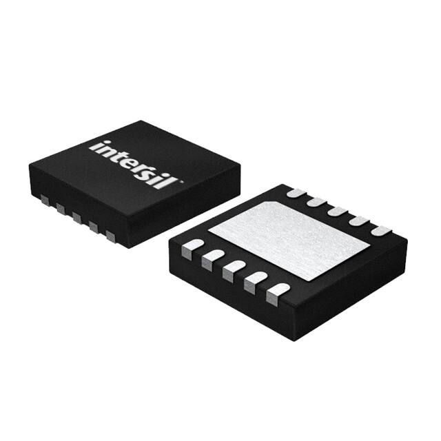
封装信息:
- 提供了多种封装类型,如8Ld SOIC、10 Ld 3x3 DFN、8 Ld EPSOIC等,以及它们的封装图纸和推荐布局。


 工商网监
湘ICP备2023018690号
工商网监
湘ICP备2023018690号
