DATASHEET
ISL6614
FN9155
Rev.5.00
May 5, 2008
Dual Advanced Synchronous Rectified Buck MOSFET Drivers with Protection
Features
The ISL6614 integrates two ISL6613 MOSFET drivers and is
specifically designed to drive two independent power
channels in a Multi-Phase interleaved buck converter
topology. These drivers combined with HIP63xx or ISL65xx
Multi-Phase Buck PWM controllers and N-Channel
MOSFETs form complete core-voltage regulator solutions for
advanced microprocessors.
The ISL6614 drives both the upper and lower gates
simultaneously over a range from 5V to 12V. This drive
voltage provides the flexibility necessary to optimize
applications involving trade-offs between gate charge and
conduction losses.
An advanced adaptive zero shoot-through protection is
integrated to prevent both the upper and lower MOSFETs
from conducting simultaneously and to minimize the dead
time. These products add an overvoltage protection feature
operational before VCC exceeds its turn-on threshold, at
which the PHASE node is connected to the gate of the low
side MOSFET (LGATE). The output voltage of the converter
is then limited by the threshold of the low side MOSFET,
which provides some protection to the microprocessor if the
upper MOSFET(s) is shorted during startup. The overtemperature protection feature prevents failures resulting
from excessive power dissipation by shutting off the outputs
when its junction temperature exceeds +150°C (typically).
The driver resets once its junction temperature returns to
+108°C (typically).
The ISL6614 also features a three-state PWM input which,
working together with Intersil’s multi-phase PWM controllers,
prevents a negative transient on the output voltage when the
output is shut down. This feature eliminates the Schottky
diode that is used in some systems for protecting the load
from reversed output voltage events.
Features
• Pin-to-pin Compatible with HIP6602 SOIC Family for
Better Performance and Extra Protection Features
• Quad N-Channel MOSFET Drives for Two Synchronous
Rectified Bridges
• Advanced Adaptive Zero Shoot-Through Protection
- Body Diode Detection
- Auto-zero of rDS(ON) Conduction Offset Effect
• Adjustable Gate Voltage (5V to 12V) for Optimal Efficiency
• Internal Bootstrap Schottky Diode
• Bootstrap Capacitor Overcharging Prevention
• Supports High Switching Frequency (up to 1MHz)
- 3A Sinking Current Capability
- Fast Rise/Fall Times and Low Propagation Delays
• Three-State PWM Input for Output Stage Shutdown
• Three-State PWM Input Hysteresis for Applications With
Power Sequencing Requirement
• Pre-POR Overvoltage +Protection
• VCC Undervoltage Protection
• Over-Temperature Protection (OTP) with +42°C Hysteresis
• Expandable Bottom Copper Pad for Enhanced Heat Sinking
• QFN Package:
- Compliant to JEDEC PUB95 MO-220 QFN - Quad Flat
No Leads - Package Outline
- Near Chip Scale Package Footprint, which Improves
PCB Efficiency and has a Thinner Profile
• Pb-free Available (RoHS compliant)
Applications
• Core Regulators for Intel® and AMD® Microprocessors
• High Current DC/DC Converters
• High Frequency and High Efficiency VRM and VRD
Related Literature
• Technical Brief TB363 “Guidelines for Handling and
Processing Moisture Sensitive Surface Mount Devices
(SMDs)”
• Technical Brief 400 and 417 for Power Train Design,
Layout Guidelines, and Feedback Compensation Design
FN9155 Rev.5.00
May 5, 2008
Page 1 of 12
�ISL6614
PWM2
PWM1
VCC
PHASE1
ISL6614CR, ISL6614CRZ, ISL6614IR, ISL6614IRZ
(16 LD QFN)
TOP VIEW
ISL6614CB, ISL6614CBZ, ISL6614IB
(14 LD SOIC)
TOP VIEW
16
15
14
13
PWM1
1
14 VCC
PWM2
2
13 PHASE1
GND
3
12 UGATE1
LGATE1
4
11 BOOT1
PVCC
5
10 BOOT2
PGND
6
9 UGATE2
PVCC 3
10 BOOT2
LGATE2
7
8 PHASE2
PGND 4
9
GND 1
12 UGATE1
LGATE1 2
11 BOOT1
5
6
7
8
NC
LGATE2
PHASE2
NC
GND
UGATE2
Ordering Information
PART NUMBER
PART MARKING
TEMP. RANGE (°C)
PACKAGE
PKG. DWG. #
ISL6614CB*
ISL6614CB
0 to +85
14 Ld SOIC
M14.15
ISL6614CBZ* (Note)
6614CBZ
0 to +85
14 Ld SOIC (Pb-free)
M14.15
ISL6614CBZA* (Note)
6614CBZ
0 to +85
14 Ld SOIC (Pb-free)
M14.15
ISL6614CR*
ISL 6614CR
0 to +85
16 Ld 4x4 QFN
L16.4x4
ISL6614CRZ* (Note)
66 14CRZ
0 to +85
16 Ld 4x4 QFN (Pb-free)
L16.4x4
ISL6614CRZA* (Note)
66 14CRZ
0 to +85
16 Ld 4x4 QFN (Pb-free)
L16.4x4
ISL6614IB*
ISL6614IB
-40 to +85
14 Ld SOIC
M14.15
ISL6614IBZ* (Note)
6614IBZ
-40 to +85
14 Ld SOIC (Pb-free)
M14.15
ISL6614IR*
ISL 6614IR
-40 to +85
16 Ld 4x4 QFN
L16.4x4
ISL6614IRZ* (Note)
66 14IRZ
-40 to +85
16 Ld 4x4 QFN (Pb-free)
L16.4x4
*Add “-T” suffix for tape and reel. Please refer to TB347 for details on reel specifications.
NOTE: These Intersil Pb-free plastic packaged products employ special Pb-free material sets; molding compounds/die attach materials and 100%
matte tin plate PLUS ANNEAL - e3 termination finish, which is RoHS compliant and compatible with both SnPb and Pb-free soldering operations.
Intersil Pb-free products are MSL classified at Pb-free peak reflow temperatures that meet or exceed the Pb-free requirements of IPC/JEDEC J
STD-020.
FN9155 Rev.5.00
May 5, 2008
Page 2 of 12
�ISL6614
Block Diagram
BOOT1
PVCC
VCC
UGATE1
OTP AND
PRE-POR OVP
FEATURES
+5V
SHOOTTHROUGH
PROTECTION
10k
PHASE1
CHANNEL 1
PVCC
PWM1
LGATE1
8k
PGND
CONTROL
LOGIC
+5V
PVCC
PGND
BOOT2
10k
UGATE2
PWM2
SHOOTTHROUGH
PROTECTION
8k
GND
PHASE2
CHANNEL 2
PVCC
LGATE2
PGND
PAD
FN9155 Rev.5.00
May 5, 2008
FOR ISL6614CR, THE PAD ON THE BOTTOM SIDE OF
THE QFN PACKAGE MUST BE SOLDERED TO THE CIRCUIT’S GROUND.
Page 3 of 12
�ISL6614
Typical Application - 4 Channel Converter Using ISL65xx and ISL6614 Gate Drivers
BOOT1
+12V
+12V
UGATE1
VCC
PHASE1
LGATE1
+5V
DUAL
DRIVER
ISL6614
VCC
VSEN
5V TO 12V
BOOT2
COMP
FB
PVCC
+12V
UGATE2
ISEN1
PGOOD
PWM1
EN
PWM2
MAIN ISEN2
CONTROL
ISL65xx
VID
PWM1
PHASE2
PWM2
LGATE2
GND
PGND
+VCORE
ISEN3
FS/DIS
PWM3
PWM4
GND
BOOT1
+12V
+12V
ISEN4
UGATE1
VCC
PHASE1
LGATE1
DUAL
DRIVER
ISL6614
PVCC
5V TO 12V
BOOT2
+12V
UGATE2
PWM1
PHASE2
PWM2
LGATE2
GND
FN9155 Rev.5.00
May 5, 2008
PGND
Page 4 of 12
�ISL6614
Absolute Maximum Ratings
Thermal Information
Supply Voltage (VCC) . . . . . . . . . . . . . . . . . . . . . . . . . . . . . . . . .15V
Supply Voltage (PVCC) . . . . . . . . . . . . . . . . . . . . . . . . . VCC + 0.3V
BOOT Voltage (VBOOT-GND). . . . . . . . . . . . . . . . . . . . . . . . . . . .36V
Input Voltage (VPWM) . . . . . . . . . . . . . . . . . . . . . . GND - 0.3V to 7V
UGATE. . . . . . . . . . . . . . . . . . . VPHASE - 0.3VDC to VBOOT + 0.3V
VPHASE - 3.5V (
很抱歉,暂时无法提供与“ISL6614CRZA-T”相匹配的价格&库存,您可以联系我们找货
免费人工找货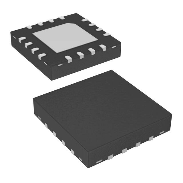


 工商网监
湘ICP备2023018690号
工商网监
湘ICP备2023018690号
