DATASHEET
ISL78236
FN8624
Rev.1.00
Mar. 14, 2017
Dual 3A Current Sharing 2.5MHz High Efficiency Synchronous Buck Regulator
The ISL78236 is a dual output, 3A/3A, integrated FET buck
regulator for point-of-load power applications. The supply
voltage range is from 2.8V to 6V, allowing for the use of a
single Li+ cell, three NiMH cells, or a regulated 3V/5V bus
input. It is optimized for regulating output voltages down to
1.2V. Each channel provides an output current up to 3A, which
can be combined to form a single 6A output in current sharing
mode. The two channels operate 180° out of phase to reduce
input RMS current and EMI.
Features
The ISL78236 integrates a pair of low ON-resistance P-channel
and N-channel internal MOSFETs to maximize efficiency and
minimize external component count. It can operate up to
100% duty cycle to maximize operating life as battery voltage
drops out. When supplying 3A on each channel, the 100% duty
cycle operation limits the dropout voltage to less than 250mV.
Other features include internal digital soft-start, independent
channel enable for power sequencing, overcurrent protection,
and thermal shutdown.
• Peak current limiting and hiccup mode short circuit
protection
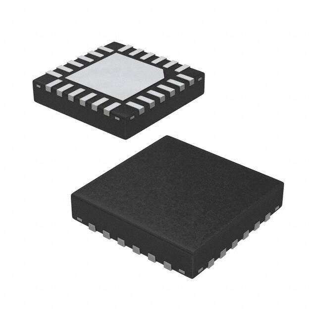
The ISL78236 is offered in a 24 Ld 4mmx4mm QFN package
with 1mm maximum height. The complete converter occupies
less than 1.5cm2 area.
• Infotainment system power
The ISL78236 is AEC - Q100 qualified and is rated for the
automotive temperature range (-40°C to +105°C).
• Dual 3A/3A independent outputs
• 2.5MHz synchronous buck regulator with internal MOSFETs
up to 95% efficiency
• 2% voltage reference accuracy over-temperature
• 6A current sharing mode operation
• Internal or external compensation
• Reverse overcurrent protection
• Over-temperature protection shutdown
• AEC-Q100 qualified
Applications
• DSP and embedded processor power supply
• Automotive point-of-load power
Related Literature
• For a full list of related documents, visit our website
- ISL78236 product page
100
2.5VOUT
3V INPUT
LX1
1.2V/3A
EN1
PG1
EN2
FPGA OR DSP
POWER
ISL78236
PG2
LX2
1.5V/3A
ASIC POWER
EFFICIENCY (%)
90
80
1.2VOUT
70
1.5VOUT
1.8VOUT
60
50
40
0.0
FIGURE 1. TYPICAL APPLICATION BLOCK DIAGRAM: DUAL OUTPUT
3A/3A BUCK REGULATOR
FN8624 Rev.1.00
Mar. 14, 2017
0.5
1.0
1.5
2.0
OUTPUT LOAD (A)
2.5
3.0
FIGURE 2. EFFICIENCY vs LOAD CURRENT, VIN = 3.3V, TA = +25°C
Page 1 of 24
�ISL78236
Table of Contents
Typical Applications . . . . . . . . . . . . . . . . . . . . . . . . . . . . . . . . . . . . . . . . . . . . . . . . . . . . . . . . . . . . . . . . . . . . . . . . . . . . . . . . . . . . . . . . . 3
Block Diagram . . . . . . . . . . . . . . . . . . . . . . . . . . . . . . . . . . . . . . . . . . . . . . . . . . . . . . . . . . . . . . . . . . . . . . . . . . . . . . . . . . . . . . . . . . . . . . 5
Pin Configuration. . . . . . . . . . . . . . . . . . . . . . . . . . . . . . . . . . . . . . . . . . . . . . . . . . . . . . . . . . . . . . . . . . . . . . . . . . . . . . . . . . . . . . . . . . . . 6
Pin Descriptions. . . . . . . . . . . . . . . . . . . . . . . . . . . . . . . . . . . . . . . . . . . . . . . . . . . . . . . . . . . . . . . . . . . . . . . . . . . . . . . . . . . . . . . . . . . . . 6
Ordering Information . . . . . . . . . . . . . . . . . . . . . . . . . . . . . . . . . . . . . . . . . . . . . . . . . . . . . . . . . . . . . . . . . . . . . . . . . . . . . . . . . . . . . . . . 7
Absolute Maximum Ratings . . . . . . . . . . . . . . . . . . . . . . . . . . . . . . . . . . . . . . . . . . . . . . . . . . . . . . . . . . . . . . . . . . . . . . . . . . . . . . . . . . 8
Thermal Information . . . . . . . . . . . . . . . . . . . . . . . . . . . . . . . . . . . . . . . . . . . . . . . . . . . . . . . . . . . . . . . . . . . . . . . . . . . . . . . . . . . . . . . . . 8
Recommended Operating Conditions . . . . . . . . . . . . . . . . . . . . . . . . . . . . . . . . . . . . . . . . . . . . . . . . . . . . . . . . . . . . . . . . . . . . . . . . . . 8
Electrical Specifications. . . . . . . . . . . . . . . . . . . . . . . . . . . . . . . . . . . . . . . . . . . . . . . . . . . . . . . . . . . . . . . . . . . . . . . . . . . . . . . . . . . . . . . . . . 8
Typical Operating Performance for Dual PWM Operation. . . . . . . . . . . . . . . . . . . . . . . . . . . . . . . . . . . . . . . . . . . . . . . . . . . . . . . . . 10
Typical Performance for Current Sharing PWM Operation . . . . . . . . . . . . . . . . . . . . . . . . . . . . . . . . . . . . . . . . . . . . . . . . . . . . . . . . 15
Theory of Operation. . . . . . . . . . . . . . . . . . . . . . . . . . . . . . . . . . . . . . . . . . . . . . . . . . . . . . . . . . . . . . . . . . . . . . . . . . . . . . . . . . . . . . . . .
PWM Control Scheme . . . . . . . . . . . . . . . . . . . . . . . . . . . . . . . . . . . . . . . . . . . . . . . . . . . . . . . . . . . . . . . . . . . . . . . . . . . . . . . . . . . . . . . . . . . .
Synchronization Control . . . . . . . . . . . . . . . . . . . . . . . . . . . . . . . . . . . . . . . . . . . . . . . . . . . . . . . . . . . . . . . . . . . . . . . . . . . . . . . . . . . . . . . . . .
Output Current Sharing . . . . . . . . . . . . . . . . . . . . . . . . . . . . . . . . . . . . . . . . . . . . . . . . . . . . . . . . . . . . . . . . . . . . . . . . . . . . . . . . . . . . . . . . . . .
Overcurrent Protection . . . . . . . . . . . . . . . . . . . . . . . . . . . . . . . . . . . . . . . . . . . . . . . . . . . . . . . . . . . . . . . . . . . . . . . . . . . . . . . . . . . . . . . . . . .
Power-Good (PG) . . . . . . . . . . . . . . . . . . . . . . . . . . . . . . . . . . . . . . . . . . . . . . . . . . . . . . . . . . . . . . . . . . . . . . . . . . . . . . . . . . . . . . . . . . . . . . . .
UVLO . . . . . . . . . . . . . . . . . . . . . . . . . . . . . . . . . . . . . . . . . . . . . . . . . . . . . . . . . . . . . . . . . . . . . . . . . . . . . . . . . . . . . . . . . . . . . . . . . . . . . . . . . .
Enable . . . . . . . . . . . . . . . . . . . . . . . . . . . . . . . . . . . . . . . . . . . . . . . . . . . . . . . . . . . . . . . . . . . . . . . . . . . . . . . . . . . . . . . . . . . . . . . . . . . . . . . . .
Soft Start-Up . . . . . . . . . . . . . . . . . . . . . . . . . . . . . . . . . . . . . . . . . . . . . . . . . . . . . . . . . . . . . . . . . . . . . . . . . . . . . . . . . . . . . . . . . . . . . . . . . . . .
Discharge Mode (Soft-Stop) . . . . . . . . . . . . . . . . . . . . . . . . . . . . . . . . . . . . . . . . . . . . . . . . . . . . . . . . . . . . . . . . . . . . . . . . . . . . . . . . . . . . . . .
Power MOSFETs . . . . . . . . . . . . . . . . . . . . . . . . . . . . . . . . . . . . . . . . . . . . . . . . . . . . . . . . . . . . . . . . . . . . . . . . . . . . . . . . . . . . . . . . . . . . . . . . .
100% Duty Cycle . . . . . . . . . . . . . . . . . . . . . . . . . . . . . . . . . . . . . . . . . . . . . . . . . . . . . . . . . . . . . . . . . . . . . . . . . . . . . . . . . . . . . . . . . . . . . . . .
Thermal Shutdown . . . . . . . . . . . . . . . . . . . . . . . . . . . . . . . . . . . . . . . . . . . . . . . . . . . . . . . . . . . . . . . . . . . . . . . . . . . . . . . . . . . . . . . . . . . . . .
18
18
18
18
18
19
19
19
19
19
19
19
19
Applications Information . . . . . . . . . . . . . . . . . . . . . . . . . . . . . . . . . . . . . . . . . . . . . . . . . . . . . . . . . . . . . . . . . . . . . . . . . . . . . . . . . . . .
Output Inductor and Capacitor Selection . . . . . . . . . . . . . . . . . . . . . . . . . . . . . . . . . . . . . . . . . . . . . . . . . . . . . . . . . . . . . . . . . . . . . . . . . . . .
Output Voltage Selection . . . . . . . . . . . . . . . . . . . . . . . . . . . . . . . . . . . . . . . . . . . . . . . . . . . . . . . . . . . . . . . . . . . . . . . . . . . . . . . . . . . . . . . . .
Minimum Output Voltage . . . . . . . . . . . . . . . . . . . . . . . . . . . . . . . . . . . . . . . . . . . . . . . . . . . . . . . . . . . . . . . . . . . . . . . . . . . . . . . . . . . . . . . . .
Input Capacitor Selection . . . . . . . . . . . . . . . . . . . . . . . . . . . . . . . . . . . . . . . . . . . . . . . . . . . . . . . . . . . . . . . . . . . . . . . . . . . . . . . . . . . . . . . . .
Loop Compensation Design . . . . . . . . . . . . . . . . . . . . . . . . . . . . . . . . . . . . . . . . . . . . . . . . . . . . . . . . . . . . . . . . . . . . . . . . . . . . . . . . . . . . . . .
PCB Layout Recommendation . . . . . . . . . . . . . . . . . . . . . . . . . . . . . . . . . . . . . . . . . . . . . . . . . . . . . . . . . . . . . . . . . . . . . . . . . . . . . . . . . . . . .
Thermal Performance . . . . . . . . . . . . . . . . . . . . . . . . . . . . . . . . . . . . . . . . . . . . . . . . . . . . . . . . . . . . . . . . . . . . . . . . . . . . . . . . . . . . . . . . . . . .
19
19
20
20
20
20
21
22
Revision History. . . . . . . . . . . . . . . . . . . . . . . . . . . . . . . . . . . . . . . . . . . . . . . . . . . . . . . . . . . . . . . . . . . . . . . . . . . . . . . . . . . . . . . . . . . . 23
About Intersil . . . . . . . . . . . . . . . . . . . . . . . . . . . . . . . . . . . . . . . . . . . . . . . . . . . . . . . . . . . . . . . . . . . . . . . . . . . . . . . . . . . . . . . . . . . . . . 23
Package Outline Drawing . . . . . . . . . . . . . . . . . . . . . . . . . . . . . . . . . . . . . . . . . . . . . . . . . . . . . . . . . . . . . . . . . . . . . . . . . . . . . . . . . . . . 24
FN8624 Rev.1.00
Mar. 14, 2017
Page 2 of 24
�ISL78236
Typical Applications
L1
0.6µH
INPUT 2.8V TO 5V
VIN1, 2
LX1
VDD
C1
2x22µF
OUTPUT
1.8V/6A
R2
124k
PGND
EN1
C3
12pF
ISL78236
EN2
FB1
R3
100k
PG1
SGND
L2
0.6µH
SYNC
LX2
PG2
SS
C2
4x22µF
PGND
C5
22nF
TO FB1
FB2
COM P
C6
150pF
R6
50k
SGND
FIGURE 3. TYPICAL APPLICATION DIAGRAM - SINGLE 6A
L1
0.6µH
INPUT 2.8V TO 5V
VIN
C1
2x22µF
LX1
C2
2x22µF
VDD
SS
EN1
OUTPUT1
1.8V/3A
PGND
R2
124k
C3
12pF
ISL78236
FB1
R3
100k
PG1
SGND
L2
0.6µH
SYN C
OUTPUT2
1.8V/3A
LX2
C4
2x22µF
EN2
PGND
R5
124k
C5
12pF
PG2
FB2
R6
100k
COMP
SGND
FIGURE 4. TYPICAL APPLICATION DIAGRAM - DUAL 3A OUTPUTS
FN8624 Rev.1.00
Mar. 14, 2017
Page 3 of 24
�ISL78236
TABLE 1. COMPONENT VALUE SELECTION FOR DUAL OUTPUT OPERATION
VOUT
1.2V
1.5V
1.8V
2.5V
3.3V
C1
2x22µF
2x22µF
2x22µF
2x22µF
2x22µF
C2
4x22µF
4X22µF
4x22µF
4x22µF
4x22µF
L1 (or L2)
0.5~1.1µH
0.5~1.1µH
0.5~1.68µH
0.5~1.68µH
0.5~2.2µH
R2 (or R5)
50k
87.5k
124k
212.5k
312.5k
R3 (or R6)
100k
100k
100k
100k
100k
TABLE 2. COMPONENT VALUE SELECTION FOR CURRENT SHARING OPERATION
VOUT
1.2V
1.5V
1.8V
2.5V
3.3V
C1
2x22µF
2x22µF
2x22µF
2x22µF
2x22µF
C2 (or C4)
2x22µF
2x22µF
2x22µF
2x22µF
2x22µF
L1 (or L2)
0.5~1.1µH
0.5~1.1µH
0.5~1.68µH
0.5~1.68µH
0.5~2.2µH
R2
50k
87.5k
124k
212.5k
312.5k
R3
100k
100k
100k
100k
100k
R6
33k
31k
30k
29k
28k
C6
180pF
150pF
150pF
150pF
150pF
FN8624 Rev.1.00
Mar. 14, 2017
Page 4 of 24
�ISL78236
Block Diagram
COMP
27pF
SS
EN1
SOFTSTAR
START
T
SHUTDOWN
BANDGAP
0.8V
0.3pF
390k
SHUTDOWN
VIN1
+
EAMP
PWM
LOGIC
CONTROLLER
PROTECTION
DRIVER
+
PWM
COMP
LX1
3pF
PGND
SLOPE
COMP
+
+
FB1
CSA1
1.6k
0.5V
0.864V
SCP
+
+
+
VIN1
OSCILLATOR
0.736V
1M
PG1
SYNC
1ms
DELAY
SGND
SHUTDOWN
THERMAL
SHUTDOWN
27pF
390k
SS
SOFTSTAR
START
T
SHUTDOWN
EN2
OCP
THRESHOLD
LOGIC
0.3pF
SHUTDOWN
VIN2
BANDGAP
0.8V
+
+
COMP
EAMP
3pF
PWM
LOGIC
CONTROLLER
PROTECTION
DRIVER
LX2
PGND
SLOPE
COMP
+
+
FB2
CSA2
1.6k
0.5V
0.864V
SCP
+
+
+
VIN2
0.736V
1M
PG2
1ms
DELAY
SGND
FIGURE 5. BLOCK DIAGRAM
FN8624 Rev.1.00
Mar. 14, 2017
Page 5 of 24
�ISL78236
Pin Configuration
LX2
PGND2
PGND2
PGND1
PGND1
LX1
ISL78236
(24 LD QFN)
TOP VIEW
24
23
22
21
20
19
LX2
1
18 LX1
VIN2
2
17 VIN1
VIN2
3
EN2
4
PG2
5
14 SS
FB2
6
13 EN1
16 VIN1
25
PAD
8
9
10
11
NC
FB1
SGND
PG1
12
SYNC
7
COMP
15 VDD
Pin Descriptions
PIN
NUMBER
SYMBOL
1, 24
LX2
Switching node connection for Channel 2.
4
EN2
Regulator Channel 2 enable pin. Enable the output, VOUT2, when driven to high. Shutdown VOUT2 and discharge output
capacitor when driven to low. Do not leave this pin floating.
5
PG2
Active high Power-Good (PG) indicator for Channel 2. After power-up or EN2 High, this output is a 1ms delayed
power-good signal for the Channel 2 output voltage.
6
FB2
The feedback network of the Channel 2 regulator. FB2 is the negative input to the transconductance error amplifier.
The output voltage is set by an external resistor divider from VOUT2 connected to FB2. The power-good output and
undervoltage lockout protection circuitry uses FB2 to monitor the Channel 1 regulator output voltage.
7
COMP
COMP pin is treated as a No Connect in dual output mode operation, using only the internal compensation. If the SS pin
is tied to a soft-start capacitor, external compensation is automatically used. An additional external network across
COMP and SGND is required to improve the loop compensation of the amplifier in parallel current sharing operation.
Connect an external RC network on COMP pin for parallel mode operation.
8
NC
No connect pin; please tie to GND for thermal relief.
9
FB1
The feedback network of the Channel 1 regulator. FB1 is the negative input to the transconductance error amplifier.
The output voltage is set by an external resistor divider from VOUT1 connected to FB1. The power-good output and
undervoltage lockout protection circuitry uses FB1 to monitor the Channel 1 regulator output voltage.
10
SGND
11
PG1
Active high Power-Good (PG) indicator for Channel 1. After power-up or EN1 High, this output is a 1ms delayed
power-good signal for the Channel 1 output voltage.
12
SYNC
Connect to logic high or input voltage VIN. Connect to an external function generator for external synchronization.
Negative edge trigger. Do not leave this pin floating. Do not tie this pin low (or to SGND).
13
EN1
Regulator Channel 1 enable pin. Enable the output, VOUT1, when driven to high. Shut down VOUT1 and discharge
output capacitor when driven to low. Do not leave this pin floating.
FN8624 Rev.1.00
Mar. 14, 2017
DESCRIPTION
System ground.
Page 6 of 24
�ISL78236
Pin Descriptions (Continued)
PIN
NUMBER
SYMBOL
DESCRIPTION
14
SS
The SS is used to adjust the soft-start time. When the SS pin is tied to VIN, SS time is 1.5ms. the SS pin is tied to VIN
only in dual output mode operation. SS pin is tied to a soft-start capacitor only in parallel current sharing mode
operation. Connect a capacitor from SS to SGND to adjust the soft-start time. CSS should not be larger than 33nF. This
capacitor, along with an internal 5µA current source, sets the soft-start interval of the converter, tSS.
(EQ. 1)
C SS F = 6.25 t SS s
15
VDD
Input supply voltage for the logic. VDD to be at the same potential as VIN +0.3/-0.5V.
16, 17
VIN1
Input supply voltage. Connect 22µF ceramic capacitor to power ground per channel.
2, 3
VIN2
18, 19
LX1
20, 21
PGND1
Negative supply for the power stage of Channel 1.
22, 23
PGND2
Negative supply for the power stage of Channel 2.
25
PAD
Switching node connection for Channel 1.
The exposed pad must be connected to the SGND pin for proper electrical performance. Add as many vias as possible
to connect the PAD to a ground plane for optimal thermal performance.
Ordering Information
PART NUMBER
(Notes 1, 2, 3)
PART
MARKING
ISL78236ARZ
782 36ARZ
ISL78236DUALEVAL1Z
Evaluation Board
ISL78236CRSHEVAL1Z
Evaluation Board
TEMP. RANGE
(°C)
-40 to +105
PACKAGE
(Pb-free)
24 Ld 4x4 QFN
PKG.
DWG. #
L24.4x4D
NOTES:
1. Add “-T” suffix for 6k unit or “-T7A” suffix for 250 unit tape and reel options. Refer to TB347 for details on reel specifications.
2. These Intersil Pb-free plastic packaged products employ special Pb-free material sets, molding compounds/die attach materials, and 100% matte
tin plate plus anneal (e3 termination finish, which is RoHS compliant and compatible with both SnPb and Pb-free soldering operations). Intersil Pbfree products are MSL classified at Pb-free peak reflow temperatures that meet or exceed the Pb-free requirements of IPC/JEDEC J STD-020.
3. For Moisture Sensitivity Level (MSL), please see product information page for ISL78236. For more information on MSL, see tech brief TB363.
FN8624 Rev.1.00
Mar. 14, 2017
Page 7 of 24
�ISL78236
Absolute Maximum Ratings
Thermal Information
(Reference to SGND)
VIN1, VIN2, VDD . . . . . . . . . . . . . . . . . . . . . . . . . . . . . . . . . . . . -0.3V to +6.5V
LX1, LX2 (Note 4) . . . . . . . . . . . . . . . . . . . . . . . . . . . . . . . . . . . . . . . -0.3V to +6.5V
EN1, EN2, PG1, PG2, SYNC, SS . . . . . . . . . . . . . . . . . . . . . . . -0.3V to +6.5V
FB1, FB2, COMP . . . . . . . . . . . . . . . . . . . . . . . . . . . . . . . . . . . . -0.3V to +2.7V
ESD Ratings
Human Body Model (Tested per AEC-Q100-002) . . . . . . . . . . . . . . . . 4kV
Machine Model (Tested per AEC-A100-003) . . . . . . . . . . . . . . . . . . . 300V
Charged Device Model (Tested per AEC-Q100-011). . . . . . . . . . . . . . 2kV
Latch Up (Per JESD-78D; Class 2, Level A; AEC-Q100-004) . . . . . . 100mA
Thermal Resistance (Typical)
JA (°C/W) JC (°C/W)
24 Ld 4x4 QFN (Notes 5, 6). . . . . . . . . . .
36
2
Junction Temperature Range . . . . . . . . . . . . . . . . . . . . . . .-55°C to +150°C
Storage Temperature Range. . . . . . . . . . . . . . . . . . . . . . . .-65°C to +150°C
Ambient Temperature Range . . . . . . . . . . . . . . . . . . . . . . . -40°C to +105°C
Pb-Free Reflow Profile . . . . . . . . . . . . . . . . . . . . . . . . . . . . . . . . . . see TB493
Recommended Operating Conditions
VIN Supply Voltage Range . . . . . . . . . . . . . . . . . . . . . . . . . . . . +2.85V to +6V
Load Current Range per Channel . . . . . . . . . . . . . . . . . . . . . . . . . . . 0A to 3A
Ambient Temperature Range . . . . . . . . . . . . . . . . . . . . . . .-40°C to +105°C
CAUTION: Do not operate at or near the maximum ratings listed for extended periods of time. Exposure to such conditions may adversely impact product
reliability and result in failures not covered by warranty.
NOTES:
4. Values shown for continuous voltage. Absolute Maximum Rating of 7V for a duration less than 20ms. Absolute Maximum Rating of -1.5V for duration
of less than 100ns.
5. JA is measured in free air with the component mounted on a high effective thermal conductivity test board with “direct attach” features. See Tech
Brief TB379.
6. JC, “case temperature” location is at the center of the exposed metal pad on the package underside.
Electrical Specifications Unless otherwise noted, the typical specifications are measured at the following conditions:
TA = -40°C to +105°C, VIN = 3.6V, EN1 = EN2 = VDD, L = 1.5µH, C1 = C2 = C4 = 2x22µF, IOUT1 = IOUT2 = 0A to 3A, unless otherwise noted. Typical values
are at TA = +25°C. Boldface limits apply across the operating temperature range, -40°C to +105°C.
PARAMETER
SYMBOL
TEST CONDITIONS
MIN
(Note 7)
TYP
MAX
(Note 7)
UNITS
2.5
2.85
V
INPUT SUPPLY
VIN Undervoltage Lockout Threshold
VUVLO
Rising
Hysteresis
40
100
mV
Quiescent Supply Current
IVDD
SYNC = VDD, EN1 = EN2 = VDD, no load at the
output
30
70
mA
Shutdown Supply Current
ISD
VIN = VDD = 6V, EN1 = EN2 = SGND
8
35
µA
0.8
0.810
V
OUTPUT REGULATION
FB1, FB2 Regulation Voltage
VFB
FB1, FB2 Bias Current
IFB
0.784
VFB = 0.75V
1
µA
Load Regulation
SYNC = VDD, output load from 0A to 6A
2
mV/A
Line Regulation
VIN = VO + 0.5V to 6V (minimal 2.85V)
0.1
%/V
Soft-start Ramp Time Cycle
SS = VDD
1.5
ms
Soft-start Charging Current
ISS
4
5
6
µA
COMPENSATION
Error Amplifier Transconductance
SS = VDD
20
µA/V
SS with Capacitor
100
µA/V
Current Sense Amplifier Gain
CSA_GAIN
0.172
Ch1/Ch2 Amplifier Gain Matching
GAINMATCH
-0.05
0.2
0.228
V/A
+0.05
V/A
OVERCURRENT PROTECTION
Dynamic Current Limit ON-time
tOCON
17
Clock pulses
Dynamic Current Limit OFF-time
tOCOFF
8
SS cycle
FN8624 Rev.1.00
Mar. 14, 2017
Page 8 of 24
�ISL78236
Electrical Specifications Unless otherwise noted, the typical specifications are measured at the following conditions:
TA = -40°C to +105°C, VIN = 3.6V, EN1 = EN2 = VDD, L = 1.5µH, C1 = C2 = C4 = 2x22µF, IOUT1 = IOUT2 = 0A to 3A, unless otherwise noted. Typical values
are at TA = +25°C. Boldface limits apply across the operating temperature range, -40°C to +105°C. (Continued)
PARAMETER
Positive Peak Overcurrent Limit
Negative Peak Overcurrent Limit
MIN
(Note 7)
TYP
MAX
(Note 7)
UNITS
Ipoc1
4.1
4.8
5.5
A
Ipoc2
4.1
4.8
5.5
A
Inoc1
-3.5
-2.5
-1.5
A
Inoc2
-3.5
-2.5
-1.5
A
VIN = 5.5V, IO = 200mA
50
75
mΩ
VIN = 2.85V, IO = 200mA
70
100
mΩ
VIN = 5.5V, IO = 200mA
50
75
mΩ
VIN = 2.85V, IO = 200mA
70
100
mΩ
SYMBOL
TEST CONDITIONS
LX1, LX2
P-Channel MOSFET ON-Resistance
N-Channel MOSFET ON-Resistance
LX_ Maximum Duty Cycle
PWM Switching Frequency
Synchronization Frequency Range
100
FS
FSYNC
2.15
(Note 8)
Channel 1 to Channel 2 Phase Shift
Rising edge to rising edge timing
LX Minimum On Time
SYNC = High (PWM mode)
Soft Discharge Resistance
RDIS
LX Leakage Current
EN = LOW
2.5
6
%
2.85
MHz
8
MHz
180
80
VIN = VDD = 6V
°
140
ns
100
120
Ω
0.1
1
µA
0.3
V
0.01
0.1
µA
PG1, PG2
Output Low Voltage
Sinking 1mA, VFB = 0.7V
PG Pin Leakage Current
PG = VIN = 6V
Internal PGOOD Low Rising Threshold
Percentage of nominal regulation voltage
88
92
95
%
Internal PGOOD Low Falling Threshold
Percentage of nominal regulation voltage
85
88
92
%
Delay Time (Rising Edge)
Time from VOUT_ reached regulation
1
Internal PGOOD Delay Time
(Falling Edge)
7
ms
15
µs
0.4
V
EN1, EN2, SYNC
Logic Input Low
Logic Input High
1.5
V
SYNC Logic Input Leakage Current
ISYNC
VIN = VDD = 6V
0.1
1
µA
Enable Logic Input Leakage Current
IEN
VIN = VDD = 6V
0.1
1
µA
Thermal Shutdown
150
°C
Thermal Shutdown Hysteresis
25
°C
NOTES:
7. Parameters with MIN and/or MAX limits are 100% tested at +25°C, unless otherwise specified. Temperature limits established by characterization and
are not production tested.
8. The operational frequency per switching channel will be half of the SYNC frequency.
FN8624 Rev.1.00
Mar. 14, 2017
Page 9 of 24
�ISL78236
Typical Operating Performance for Dual PWM Operation
Unless otherwise noted,
operating conditions are: TA = +25°C, VOUT1 = 1.8V, VOUT2 = 1.8V, IOUT1 = 0A to 3A, IOUT2 = 0A to 3A, L1 = L2 = 0.6µH, COUT1 = 2x22µF,
COUT2 = 2x22µF, FSW = 2.5MHz.
100
100
2.5VOUT
1.2VOUT
1.5VOUT
EFFICIENCY (%)
EFFICIENCY (%)
80
1.8VOUT
70
60
80
70
60
50
50
0
0.5
1.0
1.5
2.0
2.5
40
3.0
0
0.5
1.0
1.5
2.0
2.5
3.0
OUTPUT LOAD (A)
OUTPUT LOAD (A)
FIGURE 7. EFFICIENCY, VIN = 5V, TA = +25°C
FIGURE 6. EFFICIENCY, VIN = 3.3V, TA = +25°C
1.8
0.20
1.6
T = +125°C
1.4
0.15
T = +105°C
1.2
T = +25°C
1.0
DVOUT (%)
POWER DISSIPATION (W)
3.3VOUT
90
90
40
2.5VOUT
T = -40°C
0.8
0.6
0.4
DVOUT
REFERENCED FROM
VOUT AT VIN = 2.7V
0A LOAD
0.10
6A LOAD
3A LOAD
0.05
0.00
0.2
0
0
0.5
1.0
1.5
2.0
2.5
3.0
-0.05
2.5
3.0
3.5
4.0
4.5
5.0
5.5
INPUT VOLTAGE (V)
OUTPUT LOAD (A)
FIGURE 9. LINE REGULATION, VOUT = 1.8V, TA = +25°C
FIGURE 8. POWER DISSIPATION, VIN = 3.3V, VOUT = 1.8V
0
-1
DVOUT (mV)
-2
-3
-4
3.3VIN
-5
DVOUT
REFERENCED FROM
VOUT AT IOUT = 0A
-6
-7
0
0.5
1.0
1.5
2.0
2.5
3.0
OUTPUT CURRENT (A)
FIGURE 10. LOAD REGULATION, VOUT = 1.8V, TA = +25°C
FN8624 Rev.1.00
Mar. 14, 2017
Page 10 of 24
6.0
�ISL78236
Typical Operating Performance for Dual PWM Operation
Unless otherwise noted,
operating conditions are: TA = +25°C, VOUT1 = 1.8V, VOUT2 = 1.8V, IOUT1 = 0A to 3A, IOUT2 = 0A to 3A, L1 = L2 = 0.6µH, COUT1 = 2x22µF,
COUT2 = 2x22µF, FSW = 2.5MHz. (Continued)
200ns/DIV
VIN = 5V
LX1 2V/DIV
200ns/DIV
VIN = 5V
LX2 2V/DIV
VOUT RIPPLE 20mV/DIV
VOUT RIPPLE 20mV/DIV
IL1 2A/DIV
IL2 2A/DIV
FIGURE 11. STEADY STATE OPERATION AT NO LOAD CHANNEL 1
200ns/DIV
VIN = 5V
LX1 2V/DIV
FIGURE 12. STEADY STATE OPERATION AT NO LOAD CHANNEL 2
200ns/DIV
VIN = 5V
LX2 2V/DIV
VOUT RIPPLE 20mV/DIV
VOUT RIPPLE 20mV/DIV
IL1 2A/DIV
IL2 2A/DIV
FIGURE 13. STEADY STATE OPERATION AT 3A LOAD CHANNEL 1
VOUT1 RIPPLE 100mV/DIV
VIN = 5V
VIN = 5V
100µs/DIV
CH2 IOUT = 0A
100µs/DIV
CH1 IOUT = 0A
IL1 2A/DIV
FIGURE 15. LOAD TRANSIENT CHANNEL 1
FN8624 Rev.1.00
Mar. 14, 2017
FIGURE 14. STEADY STATE OPERATION AT 3A LOAD CHANNEL 2
VOUT2 RIPPLE 100mV/DIV
IL2 2A/DIV
FIGURE 16. LOAD TRANSIENT CHANNEL 2
Page 11 of 24
�ISL78236
Typical Operating Performance for Dual PWM Operation
Unless otherwise noted,
operating conditions are: TA = +25°C, VOUT1 = 1.8V, VOUT2 = 1.8V, IOUT1 = 0A to 3A, IOUT2 = 0A to 3A, L1 = L2 = 0.6µH, COUT1 = 2x22µF,
COUT2 = 2x22µF, FSW = 2.5MHz. (Continued)
VIN = 3.3V
VIN = 3.3V
EN1
VOUT
EN2
VOUT
LX1 VOLTAGE
LX2 VOLTAGE
PG1
PG2
FIGURE 17. SOFT-START WITH NO LOAD CHANNEL 1
EN1
VIN = 3.3V
EN2
VIN = 3.3V
VOUT
VOUT
LX1 VOLTAGE
LX2 VOLTAGE
PG1
PG2
FIGURE 20. SOFT-START AT 3A LOAD CHANNEL 2
FIGURE 19. SOFT-START AT 3A LOAD CHANNEL 1
VIN = 3.3V
VIN = 3.3V
EN1
EN2
VOUT
VOUT
LX1 VOLTAGE
LX2 VOLTAGE
PG1
PG2
FIGURE 21. SOFT-DISCHARGE SHUTDOWN CHANNEL 1
FN8624 Rev.1.00
Mar. 14, 2017
FIGURE 18. SOFT-START WITH NO LOAD CHANNEL 2
FIGURE 22. SOFT-DISCHARGE SHUTDOWN CHANNEL 2
Page 12 of 24
�ISL78236
Typical Operating Performance for Dual PWM Operation
Unless otherwise noted,
operating conditions are: TA = +25°C, VOUT1 = 1.8V, VOUT2 = 1.8V, IOUT1 = 0A to 3A, IOUT2 = 0A to 3A, L1 = L2 = 0.6µH, COUT1 = 2x22µF,
COUT2 = 2x22µF, FSW = 2.5MHz. (Continued)
200ns/DIV
VIN = 5V
LX1 2V/DIV
200ns/DIV
VIN = 5V
SYNC
SYNC
VOUT2 RIPPLE 50mV/DIV
VOUT1 RIPPLE 50mV/DIV
FIGURE 23. STEADY STATE OPERATION CHANNEL 1 AT NO LOAD
WITH FSW = 4MHz
200ns/DIV, VIN = 5V
LX1 2V/DIV
FIGURE 24. STEADY STATE OPERATION CHANNEL 2 AT NO LOAD
WITH FSW = 4MHz
200ns/DIV, VIN = 5V
SYNC
VOUT2 RIPPLE 50mV/DIV
OUT1 2A/DIV
OUT2 2A/DIV
FIGURE 26. STEADY STATE OPERATION CHANNEL2 3A LOAD WITH
FSW = 4MHz
VIN = 5V
VIN = 5V
LX2 2V/DIV
SYNC
VOUT1 RIPPLE 50mV/DIV
FIGURE 25. STEADY STATE OPERATION CHANNEL1 3A LOAD WITH
FSW = 4MHz
LX2 2V/DIV
LX1 5V/DIV
LX1 5V/DIV
VOUT1 1V/DIV
IL1 1A/DIV
VOUT1 1V/DIV
IL1 1A/DIV
PG1 5V/DIV
FIGURE 27. OUTPUT SHORT CIRCUIT CHANNEL 1
FN8624 Rev.1.00
Mar. 14, 2017
PG1 5V/DIV
FIGURE 28. OUTPUT SHORT CIRCUIT RECOVERY (FROM HICCUP)
CHANNEL 1
Page 13 of 24
�ISL78236
Typical Operating Performance for Dual PWM Operation
Unless otherwise noted,
operating conditions are: TA = +25°C, VOUT1 = 1.8V, VOUT2 = 1.8V, IOUT1 = 0A to 3A, IOUT2 = 0A to 3A, L1 = L2 = 0.6µH, COUT1 = 2x22µF,
COUT2 = 2x22µF, FSW = 2.5MHz. (Continued)
VIN = 5V
VIN = 5V
LX2 5V/DIV
LX2 5V/DIV
VOUT2 1V/DIV
VOUT2 0.5V/DIV
IL2 1A/DIV
PG2 5V/DIV
FIGURE 29. OUTPUT SHORT CIRCUIT CHANNEL 2
PG2 5V/DIV
FIGURE 30. OUTPUT SHORT CIRCUIT RECOVERY (FROM HICCUP)
CHANNEL 2
1V/DIV
1V/DIV
4ns/DIV
4ns/DIV
FIGURE 32. LX JITTER AT 3A LOAD, VIN = 3V
FIGURE 31. LX JITTER AT NO LOAD, VIN = 3V
FIGURE 33. LX JITTER AT NO LOAD, VIN = 5V
FN8624 Rev.1.00
Mar. 14, 2017
IL2 1A/DIV
1V/DIV
1V/DIV
4ns/DIV
4ns/DIV
FIGURE 34. LX JITTER AT 3A LOAD, VIN = 5V
Page 14 of 24
�ISL78236
Typical Performance for Current Sharing PWM Operation
Unless otherwise noted,
operating conditions are: TA = +25°C, VOUT = 1.8V, IOUT1 + IOUT2 = 0A to 6A, L1 = L2 = 0.6µH, COUT = 4x22µF, FSW = 2.5MHz.
100
100
90
90
1.5VOUT
EFFICIENCY (%)
EFFICIENCY (%)
2.5VOUT
80
1.8VOUT
1.2VOUT
70
60
80
2.5VOUT
70
60
50
50
40
3.3VOUT
0
1
2
3
4
5
40
6
0
1
2
OUTPUT LOAD (A)
3
4
5
6
OUTPUT LOAD (A)
FIGURE 36. EFFICIENCY vs LOAD, VIN = 5V, TA = +25°C
FIGURE 35. EFFICIENCY vs LOAD, VIN = 3.3V, TA = +25°C
0.40
4.0
0.35
0.30
3.0
T = +125°C
DVOUT (%)
POWER DISSIPATION (W)
3.5
DVOUT
REFERENCED FROM
VOUT AT VIN = 2.7V
T = +105°C
2.5
2.0
T = +25°C
T = -40°C
1.5
0A LOAD
0.25
6A LOAD
0.20
0.15
3A LOAD
0.10
1.0
0.05
0.5
0
0
2.5
0
1
2
3
4
5
6
OUTPUT LOAD (A)
3.0
3.5
4.0
4.5
5.0
5.5
INPUT VOLTAGE (V)
FIGURE 38. LINE REGULATION, VOUT = 1.8V, TA = +25°C
FIGURE 37. POWER DISSIPATION, VIN = 3.3V, VOUT = 1.8V
0
-1
DVOUT (mV)
-2
3.3VIN
-3
-4
-5
-6
-7
-8
0
DVOUT
REFERENCED FROM
VOUT AT IOUT = 0A
1
2
3
4
OUTPUT CURRENT (A)
5
6
FIGURE 39. LOAD REGULATION, VOUT = 1.8V, TA = +25°C
FN8624 Rev.1.00
Mar. 14, 2017
Page 15 of 24
6.0
�ISL78236
Typical Performance for Current Sharing PWM Operation
Unless otherwise noted,
operating conditions are: TA = +25°C, VOUT = 1.8V, IOUT1 + IOUT2 = 0A to 6A, L1 = L2 = 0.6µH, COUT = 4x22µF, FSW = 2.5MHz. (Continued)
VIN = 5V
VOUT RIPPLE 100mV/DIV
VIN = 5V
VOUT RIPPLE 50mV/DIV
LX1 5V/DIV
LX1 5V/DIV
LX2 5V/DIV
LX2 5V/DIV
200ns/DIV
200ns/DIV
FIGURE 41. STEADY STATE OPERATION AT 6A LOAD
FIGURE 40. STEADY STATE OPERATION AT NO LOAD
VIN = 5V
VIN = 3.3V
VOUT RIPPLE 200mV/DIV
EN
OUTPUT CURRENT 2A/DIV
VOUT
LX1 VOLTAGE
PG1
200µs/DIV
FIGURE 42. LOAD TRANSIENT RESPONSE
VIN = 3.3V
FIGURE 43. SOFT-DISCHARGE SHUTDOWN
EN
VIN = 3.3V
EN
VOUT
LX1 VOLTAGE
VOUT
LX1 VOLTAGE
PG1
FIGURE 44. SOFT-START AT NO LOAD
FN8624 Rev.1.00
Mar. 14, 2017
PG1
FIGURE 45. SOFT-START AT 6A LOAD
Page 16 of 24
�ISL78236
Typical Performance for Current Sharing PWM Operation
Unless otherwise noted,
operating conditions are: TA = +25°C, VOUT = 1.8V, IOUT1 + IOUT2 = 0A to 6A, L1 = L2 = 0.6µH, COUT = 4x22µF, FSW = 2.5MHz. (Continued)
VIN = 5V
IL2 1A/DIV
IL2 1A/DIV
LOAD RAMP = 6A/ms
FIGURE 46. CURRENT SHARE BALANCING, 0A TO 6A
FN8624 Rev.1.00
Mar. 14, 2017
VIN = 5V
IL2 1A/DIV
IL2 1A/DIV
LOAD RAMP = 6A/ms
FIGURE 47. CURRENT SHARE BALANCING, 2A TO 6A
Page 17 of 24
�ISL78236
Theory of Operation
The ISL78236 is a dual 3A or single current sharing 6A step-down
switching regulator optimized for low output ripple point-of-load
power in automotive applications. The regulator operates at a
2.5MHz internally fixed switching frequency allowing small output
filter components while maintaining up to 95% efficiency. The two
channels are 180° out of phase operation to reduce input ripple
currents and EMI. The supply current is typically only 8µA when the
regulator is shut down.
PWM Control Scheme
Pulling the SYNC pin HI (>1.5V) forces the converter into PWM mode
in the next switching cycle regardless of output current. Each of the
channels of the ISL78236 employ the current-mode pulse-width
modulation (PWM) control scheme for fast transient response and
pulse-by-pulse current limiting, as shown in Figure 5 on page 5 with
waveforms in Figure 48. The current loop consists of the oscillator,
the PWM COMP comparator, current sensing circuit, and the slope
compensation for the current loop stability. The current-sensing
circuit consists of the resistance of the P-channel MOSFET when it is
turned on and the current sense amplifier CSA. The gain for the
current-sensing circuit is typically 0.2V/A. The control reference for
the current loops comes from the error amplifier, EAMP, of the
voltage loop.
The PWM operation is initialized by the clock from the oscillator.
The P-channel MOSFET is turned on at the beginning of a PWM
cycle and the current in the MOSFET starts to ramp up. When the
sum of the current amplifier CSA1 (or CSA2 on Channel 2) and the
compensation slope (0.46V/µs) reaches the control reference of
the current loop, the PWM COMP comparator sends a signal to the
PWM logic to turn off the P-MOSFET and to turn on the N-channel
MOSFET. The N-MOSFET stays on until the end of the PWM cycle.
Figure 48 shows the typical operating waveforms during the PWM
operation. The dotted lines illustrate the sum of the compensation
ramp and the current sense amplifier CSA_ output.
voltage loop is internally compensated with the 27pF and 390kΩ
RC network. The maximum EAMP voltage output is precisely
clamped to the bandgap voltage (1.172V).
Synchronization Control
The synchronization frequency can be operated to a range of
6MHz to 8MHz by an external signal applied to the SYNC pin. The
SYNC pin has logic threshold levels of 0.4V and 1.5V for LOW and
HIGH respectively, to allow for external clock signals to be of
different magnitude regardless of supply voltage to the
ISL78236. The first falling edge on the SYNC triggers the rising
edge of the PWM ON pulse of Channel 1. The second falling edge
of the SYNC triggers the rising edge of the PWM ON pulse of
Channel 2. Typically, the pulse width of the SYNC signal should be
50% duty cycle, however, it is recommended that the pulse width
be in the range of 50ns to 100ns for valid synchronization. This
process alternates indefinitely allowing 180°output phase
operation between the two channels. It is important to note that
this operation makes the switching frequency of each channel
1/2 of the SYNC frequency. Thus, Channel 1 and Channel 2 have
a synchronized switching frequency of 3MHz to 4MHz.
Output Current Sharing
The ISL78236 dual outputs are paralleled for multi-phase
operation in order to support 6A output. Channel 1 and Channel
2 switches 180° out of phase to reduce input ripple currents. In
parallel configuration, external soft-start should be used to
ensure proper, full loading start-up. Connect the FBx pins
together and connect a soft-start capacitor from SS pin to GND.
External compensation using the COMP pin is required for
current sharing operation. See Table 2 for recommended values
in current sharing mode. The current sharing balancing is
dependent on the current sense amplifier matching between the
two channels. The matching is internally trimmed and provides
excellent balancing of output currents. See Figures 46 and 47 for
typical output current matching.
Overcurrent Protection
VEAMP
CSA1 and CSA2 are used to monitor Output 1 and Output 2
channels respectively. The overcurrent protection is realized by
monitoring the CSA output with the OCP threshold logic, as
shown in the Figure 5 on page 5. The current sensing circuit has a
gain of 0.2V/A, from the P-MOSFET current to the CSA output.
When the CSA output reaches the threshold, the OCP comparator
is tripped to turn off the P-MOSFET immediately. The overcurrent
function protects the switching converter from a shorted output by
monitoring the current flowing through the upper MOSFETs.
VCSA1
Duty
Cycle
IL
VOUT
FIGURE 48. PWM OPERATION WAVEFORMS
The output voltage is regulated by controlling the reference
voltage to the current loop. The bandgap circuit outputs a 0.8V
reference voltage to the voltage control loop. The feedback
voltage signal comes from the FB pin. The soft-start block only
affects the operation during the start-up and will be discussed
separately. The error amplifier is a transconductance amplifier
that converts the voltage error signal to a current output. The
FN8624 Rev.1.00
Mar. 14, 2017
Upon detection of overcurrent condition, the upper MOSFET will
be immediately turned off and will not be turned on again until
the next switching cycle. Upon detection of the initial overcurrent
condition, the Overcurrent Fault Counter is set to 1 and the
Overcurrent Condition Flag is set from LOW to HIGH. If, on the
subsequent cycle, another overcurrent condition is detected, the
OC Fault Counter will be incremented. If there are 17 sequential
OC fault detections, the regulator will be shut down under an
Overcurrent Fault Condition. An Overcurrent Fault Condition will
result in the regulator attempting to restart in a hiccup mode
with the delay between restarts being eight soft-start periods. At
the end of the eighth soft-start wait period, the fault counters are
Page 18 of 24
�ISL78236
reset and soft-start is attempted again. If the overcurrent
condition goes away prior to the OC Fault Counter reaching a
count of four, the Overcurrent Condition Flag will set back to
LOW.
The ISL78236 also features current sense amplifiers on the
N-MOSFET for Negative Overcurrent Protection. If the negative
output current reaches -2.5A, the part enters Negative OCP. At
this point, all switching stops and the part enters tri-state mode
while the pull-down FET is discharging the output until it reaches
normal regulation voltage, then the IC restarts.
Discharge Mode (Soft-Stop)
When a transition to shutdown mode occurs, or the input UVLO
fault latch is set, the LX pin discharges to PGND through an
internal 100Ω switch.
Power MOSFETs
The integrated high-side and low-side power MOSFETs are
optimized for best efficiency while delivering up to 3A current.
The ON-resistance for the P-MOSFET is typically 50mΩ and the
ON-resistance for the N-MOSFET is typical 50mΩ.
Power-Good (PG)
100% Duty Cycle
There are two independent power-good signals. PG1 monitors
the Output Channel 1 and PG2 monitors the Output Channel 2.
When powering up, the open-collector power-good output holds
low for about 1ms after the output reaches within 8% of the
preset output voltage. The PG pin will pull low under fault
conditions when an overcurrent, OTP, or UVLO event occurs.
The ISL78236 features 100% duty cycle operation to maximize
the battery life in portable applications. When the battery voltage
drops to a level at which the ISL78236 can no longer maintain
the regulation at the output, the regulator completely turns on
the P-MOSFET. The maximum dropout voltage under the 100%
duty cycle operation is the product of the load current and the
ON-resistance of the P-MOSFET.
UVLO
When the input voltage is below the undervoltage lockout (UVLO)
threshold (2.85V MAX), the regulator is disabled and the PG pin
will pull low.
Enable
The enable (ENx) inputs allow the user to control turning on or off
each channel of the regulator for purposes such as low power
shutdown or power-up sequencing. When the regulator is
enabled, there is typically a 600µs delay for waking up the
bandgap reference, afterwards the soft start-up sequence
begins.
Soft Start-Up
The soft-start-up eliminates the in-rush current during the
start-up. The soft-start block outputs a ramp reference to both
the voltage loop and the current loop. The two ramps limit the
inductor current rising speed as well as the output voltage speed
so that the output voltage rises in a controlled fashion. When the
FB voltage is less than 0.2V, the PWM operating frequency is half
of the normal frequency.
When the SS soft-start pin is tied to the VIN pin, the soft start-up
time is internally set to 1.5ms. This internal soft-start mode is
only for dual output operation. In current sharing mode, for
externally programmable soft-start time, connect a capacitor
from the SS pin to GND. A 5µA current source charges up the
soft-start capacitor and sets the soft-start ramp time. The
soft-start capacitor, CSS, should not be larger than 33nF. See
Equation 2 for calculating the soft-start ramp time.
It is recommended to operate the internal soft-start ramp time
only in Dual Output Mode. In Current Share Mode, external
soft-start should be used.
C SS F
t SS S = ----------------------6.25
FN8624 Rev.1.00
Mar. 14, 2017
Thermal Shutdown
The ISL78236 has built-in thermal protection. When the internal
temperature reaches +150°C, the regulator is completely shut
down. As the temperature drops to +125°C, the ISL78236 resumes
operation by stepping through a soft start-up.
Applications Information
Output Inductor and Capacitor Selection
To consider steady state and transient operation, ISL78236
typically uses a 0.6µH output inductor. Higher or lower inductor
value can be used to optimize the total converter system
performance. For example applications with output voltage
>3.3V, in order to decrease the inductor current ripple and output
voltage ripple, the output inductor value can be increased. The
inductor ripple current can be expressed in Equation 3:
VO
V O 1 – ---------
V IN
I = --------------------------------------L fS
(EQ. 3)
The inductor’s saturation current rating needs to be larger than
the peak current. The ISL78236 overcurrent protection threshold
is typically 4.8A. The saturation current needs to be over 4.8A for
maximum output current application.
ISL78236 uses an internal compensation network and the output
capacitor value is dependent on the output voltage. The ceramic
capacitor is recommended to be X5R or X7R. The recommended
minimum output capacitor values for the ISL78236 are shown in
Table 3.
(EQ. 2)
Page 19 of 24
�ISL78236
regulator. The value for the feedback resistor is typically between
50kΩ and 312.5kΩ. Setting R2 and VOUT, R3 will be:
TABLE 3. MINIMUM OUTPUT CAPACITOR VALUE vs VOUT
VOUT
(V)
COUT
(µF)
L
(µH)
1.2
2 x 22
0.5~1.1
1.6
2 x 22
0.5~1.1
1.8
2 x 22
0.5~1.68
2.5
2 x 22
0.5~1.68
3.3
2 x 6.8
0.5~2.2
3.6
10
0.5~2.2
R 2 x0.8V
R 3 = ---------------------------------V OUT – 0.8V
For better performance, add 12pF in parallel with R2 (or R5) for
faster transient response
Minimum Output Voltage
In Table 3, the minimum output capacitor value is given for
different output voltages to make sure the converter system is
stable.
Although ceramic capacitors offer excellent overall performance
and reliability, the actual in-circuit capacitance must be
considered. Ceramic capacitors are rated using large
peak-to-peak voltage swings and with no DC bias. In the DC/DC
converter application, these conditions do not reflect reality. As a
result, the actual capacitance may be considerably lower than
the advertised value. Consult the manufacturer’s datasheet to
determine the actual in-application capacitance. Most
manufacturers publish capacitance vs DC bias so that this effect
can be easily accommodated. The effects of AC voltage are not
frequently published, but an assumption of ~20% further
reduction will generally suffice. The result of these
considerations may mean an effective capacitance 50% lower
than nominal and this value should be used in all design
calculations. Nonetheless, ceramic capacitors are a very good
choice in many applications due to their reliability and extremely
low ESR.
Equations 4 and 5 allow calculation of the required capacitance
to meet a desired ripple voltage level. Additional capacitance
may be used.
For the ceramic capacitors (low ESR):
I
V OUTripple = --------------------------------------8 F SW C OUT
(EQ. 6)
(EQ. 4)
where I is the inductor’s peak-to-peak ripple current, FSW is the
switching frequency, and COUT is the output capacitor.
The ISL78236 switching frequency FS (2.5MHz typical,
2.85MHz max) and the minimum LX pin ON Time (140ns, max)
sets a minimum duty cycle of the converter under worst-case
scenario of 0.4 across temperature. Because of this minimum
duty cycle, the ISL78236 is capable of regulating to an input VIN
to output VOUT range. The ratio of output to input (VOUT/VIN)
must be higher than 0.4 to maintain output voltage regulation.
For example, it is not recommended to regulate below 2.0V for
VIN = 5V and below 1.2V for VIN = 3V as the minimum duty cycle
limitation will impact output voltage. Note that when external
synchronization is used, the switching frequency is higher than
2.85MHz which further restricts the VOUT/VIN range of operation.
Input Capacitor Selection
The main functions for the input capacitor are to provide
decoupling of the parasitic inductance and to provide a filtering
function to prevent the switching current flowing back to the
battery rail. One 22µF X5R or X7R ceramic capacitor is a good
starting point for the input capacitor selection per channel.
Loop Compensation Design
When a soft-start capacitor is connected to the SS pin, the COMP
pin is active for external loop compensation. The ISL78236 uses
constant frequency peak current mode control architecture to
achieve a fast loop transient response. An accurate current
sensing pilot device in parallel with the upper MOSFET is used for
peak current control signal and overcurrent protection. The
inductor is not considered as a state variable since its peak
current is constant, and the system becomes a single order
system. It is much easier to design a Type II compensator to
stabilize the loop than to implement voltage mode control. Peak
current mode control has an inherent input voltage feed-forward
function to achieve good line regulation. Figure 49 shows the
small signal model of the synchronous buck regulator.
If using electrolytic capacitors, then:
V OUTripple = I*ESR
(EQ. 5)
Output Voltage Selection
The output voltage of the regulator can be programmed via an
external resistor divider, which is used to scale the output voltage
relative to the internal reference voltage and feed it back to the
inverting input of the error amplifier. Refer to Figures 3 and 4.
The output voltage programming resistor, R2 (or R5 in
Channel 2), will depend on the desired output voltage of the
FN8624 Rev.1.00
Mar. 14, 2017
Page 20 of 24
�ISL78236
+
^
iin
^
iL LP
RLP
d^
ILd^ 1:D Vin
^
Vin
+
2f c V o C o R t
3
R 6 = ---------------------------------- = 15.7 10 f c V o C o
GM V FB
Ro
Where Rt is the current sense amplifier gain (0.2V/A) and GM is
the transconductance, gm, of the voltage error amplifier in each
phase (see “Electrical Specification” Table for “Error Amplifier
Transconductance” on page 8). Compensator capacitor C6 and
C7 is then given by Equation 9.
Rc
RT
GAIN (VLOOP (S(fi))
vo^
Co
Ti(S)
d^
Ro Co Vo Co
Rc Co 1
C 6 = --------------- = --------------- ,C 7 = max of (--------------,----------------)
R6
Io R6
R 6 f s R 6
K
Fm
+
v^comp
-Av(S)
FIGURE 49. SMALL SIGNAL MODEL OF SYNCHRONOUS BUCK
REGULATOR
Vo
R2
C3
VFB
R3
VREF
1
C 3 = ---------------f c R 2
(EQ. 10)
Example: VIN = 5V, VO = 1.8V, IO = 3A, Fs = 2.5MHz, R2 = 124kΩ,
R3 = 100kΩ, Co = 2X22µF/3mΩ, L = 0.6µH, fc = 100kHz, then
compensator resistance R6:
3
R 6 = 15.7 10 100kHz 1.8V 44F = 124k
-
(EQ. 9)
An optional zero can boost the phase margin. CZ2 is a zero due
to R2 and C3
Tv(S)
He(S)
(EQ. 8)
VCOMP
(EQ. 11)
Use a standard 124kΩ 1% tolerance or better resistor.
GM
+
R6
1.8V 44 F
C 6 = -------------------------------- = 213pF
3A 124k
(EQ. 12)
3m 44F-,---------------------------------------------------1
C 7 = max (-------------------------------) = (1pF,1pF)
124k
2.5MHz 124k
(EQ. 13)
C7
C6
Use the closest standard values for C6 and C7. There is
approximately 2pF parasitic capacitance from VCOMP to GND;
Therefore, C7 is optional. Use C6 = 220pF and C7 = OPEN.
FIGURE 50. TYPE II COMPENSATOR
Figure 50 shows the Type II compensator with its transfer
function expressed, as shown in Equation 7:
1
C 3 = ---------------------------------------------------- = 26pF
100kHz 124k
S
S
1 + ------------ 1 + -------------
GM R 3
cz1
cz2
vˆ COMP
- = -------------------------------------------------------- --------------------------------------------------------------A v S = ------------------ C6 + C7 R2 + R3
S
S
vˆ FB
S 1 + ------------- 1 + -------------
Use C3 = 22pF. Note that C3 may increase the loop bandwidth
from previous estimated value.
cp1
cp2
(EQ. 7)
where,
R2 + R3
C6 + C7
1
1
cz1 = --------------- , cz2 = --------------- cp1 = ----------------------- cp2 = ----------------------R6 C6 C7
C3 R2 R3
R6 C6
R2 C3
Compensator design goal:
High DC gain
Choose loop bandwidth fc 100kHz or below
Gain margin: >10dB
Phase margin: >40°
The compensator design procedure is as follows:
The loop gain at crossover frequency of fc has a unity gain.
Therefore, the compensator resistance R6 is determined by
Equation 8.
FN8624 Rev.1.00
Mar. 14, 2017
(EQ. 14)
PCB Layout Recommendation
The PCB layout is a very important converter design step to make
sure the designed converter works well. For ISL78236, the power
loop is composed of the output inductor L’s, the output capacitor
COUT1 and COUT2, the LX’s pins, and the PGND pin. It is necessary to
make the power loop as small as possible and the connecting traces
among them should be direct, short, and wide. The switching node
of the converter, the LX pins, and the traces connected to the node
are very noisy, so keep the voltage feedback trace away from these
noisy traces. The FB network should be as close as possible to its FB
pin. SGND should have one single connection to PGND. The input
capacitor should be placed as closely as possible to the VIN pin.
Also, the ground of the input and output capacitors should be
connected as closely as possible. The heat of the IC is mainly
dissipated through the thermal pad. Maximizing the copper area
connected to the thermal pad is preferable. In addition, a solid
ground plane is helpful for better EMI performance. It is
recommended to add at least five vias ground connection within
the pad for the best thermal relief.
Page 21 of 24
�ISL78236
Thermal Performance
PGND2
PGND2
PGND1
PGND1
LX1
24
23
22
21
20
19
LX2
1
18 LX1
VIN2
2
17 VIN1
VIN2
3
EN2
4
PG2
5
14 SS
FB2
6
13 EN1
16 VIN1
25
PAD
7
8
9
10
11
12
FB1
SGND
PG1
SYNC
15 VDD
NC
It is essential to have the package thermal pad connected to a
top layer PCB ground pad with the via connecting to additional
ground planes. This is where most of the thermal relief will occur.
The four PGND pins of the ISL78236 should be connected to the
thermal pad also. These connections provide the extra thermal
relief to minimize theta JA allowing the ISL78236 to maintain full
output current up to +105°C. See Figure 51 for an example
layout of the thermal relief pad.
LX2
The theta JA (JA) spec shown in the “Thermal Information” on
page 8 is based upon JEDEC standard JESD51-5. However, real
world application boards will differ from the JEDEC standard,
thus producing different theta JA results. For example, the
JESD51-5 specifies the thermal attach pad via only to the top
buried layer. Most practical applications will have the via connect
to all layers of the PCB board ground plane. JESD51-5 also
requires that buried planes use 1 oz. copper while the outer
planes use 2 oz. copper. It is recommended to have 2 oz. or
greater copper on all layers in application boards.
PIN 1
COMP
Delivering a full load output current of 6A across the ambient
operating temperature is strongly dependent on the thermal
characteristic of the PCB layout. The power dissipation of the IC
and the thermal impedance of the board will result in a
temperature gradient between ambient and junction. Power
dissipation curves for typical application can be found in
Figures 8 and 9 for dual output operation and Figures 37 and 38
for current sharing operation. If the junction temperature
exceeds the +150°C over-temperature protection threshold the
regulator will be disabled.
FIGURE 51. RECOMMENDED THERMAL PAD LAYOUT
FN8624 Rev.1.00
Mar. 14, 2017
Page 22 of 24
�ISL78236
Revision History
The revision history provided is for informational purposes only and is believed to be accurate, but not warranted.
Please visit our website to make sure you have the latest revision.
DATE
REVISION
CHANGE
January 30, 2017
FN8624.1
Updated Typical Performance Curves as follows:
Figure 6: Remove red curve for Vout=1.8V operation.
Remove Figure 8: Power Dissipation, Vin=5V, Vout=1.8V
Figure 10: Remove red curve Vin=5V operation
Figure 36: Remove pink curve Vout=1.8V operation.
Remove Figure 38: Power Dissipation, Vin=5V, Vout=1.8V
Figure 40: Remove red curve Vin=5V operation
April 28, 2014
FN8624.0
Initial Release
About Intersil
Intersil Corporation is a leading provider of innovative power management and precision analog solutions. The company's products
address some of the largest markets within the industrial and infrastructure, mobile computing, and high-end consumer markets.
For the most updated datasheet, application notes, related documentation, and related parts, see the respective product information
page found at www.intersil.com.
For a listing of definitions and abbreviations of common terms used in our documents, visit: www.intersil.com/glossary.
You can report errors or suggestions for improving this datasheet by visiting www.intersil.com/ask.
Reliability reports are also available from our website at www.intersil.com/support.
© Copyright Intersil Americas LLC 2014-2017. All Rights Reserved.
All trademarks and registered trademarks are the property of their respective owners.
For additional products, see www.intersil.com/en/products.html
Intersil Automotive Qualified products are manufactured, assembled and tested utilizing TS16949 quality systems as noted
in the quality certifications found at www.intersil.com/en/support/qualandreliability.html
Intersil products are sold by description only. Intersil may modify the circuit design and/or specifications of products at any time without notice, provided that such
modification does not, in Intersil's sole judgment, affect the form, fit or function of the product. Accordingly, the reader is cautioned to verify that datasheets are
current before placing orders. Information furnished by Intersil is believed to be accurate and reliable. However, no responsibility is assumed by Intersil or its
subsidiaries for its use; nor for any infringements of patents or other rights of third parties which may result from its use. No license is granted by implication or
otherwise under any patent or patent rights of Intersil or its subsidiaries.
For information regarding Intersil Corporation and its products, see www.intersil.com
FN8624 Rev.1.00
Mar. 14, 2017
Page 23 of 24
�ISL78236
Package Outline Drawing
For the most recent package outline drawing, see L24.4x4D.
L24.4x4D
24 LEAD QUAD FLAT NO-LEAD PLASTIC PACKAGE
Rev 3, 11/13
4.00
4X 2.5
A
20X 0.50
B
PIN 1
INDEX AREA
PIN #1 CORNER
(C 0 . 25)
24
19
1
18
4.00
2.45 (+ 0.10mm)
(- 0.15mm)
13
0.15
(4X)
12
7
0.10 M C A B
0 . 07
24X 0 . 23 +- 0
. 05 4
24X 0 . 4 ± 0 . 1
TOP VIEW
BOTTOM VIEW
SEE DETAIL "X"
0.10 C
C
0 . 90 ± 0 . 1
BASE PLANE
( 3 . 8 TYP )
SEATING PLANE
0.08 C
SIDE VIEW
(
2 . 50 )
( 20X 0 . 5 )
C
0 . 2 REF
5
( 24X 0 . 25 )
0 . 00 MIN.
0 . 05 MAX.
( 24X 0 . 6 )
DETAIL "X"
TYPICAL RECOMMENDED LAND PATTERN
NOTES:
1. Dimensions are in millimeters.
Dimensions in ( ) for Reference Only.
2. Dimensioning and tolerancing conform to AMSE Y14.5m-1994.
3. Unless otherwise specified, tolerance : Decimal ± 0.05
4. Dimension b applies to the metallized terminal and is measured
between 0.15mm and 0.30mm from the terminal tip.
5. Tiebar shown (if present) is a non-functional feature.
6. The configuration of the pin #1 identifier is optional, but must be
located within the zone indicated. The pin #1 identifier may be
either a mold or mark feature.
FN8624 Rev.1.00
Mar. 14, 2017
Page 24 of 24
�


 工商网监
湘ICP备2023018690号
工商网监
湘ICP备2023018690号
