DATASHEET
ISL78420
FN8296
Rev 4.00
September 29, 2016
100V, 2A Peak, Half-Bridge Driver with Tri-Level PWM Input and Adjustable
Dead-Time
The ISL78420 is a 100V, 2A high frequency half-bridge NMOS
FET driver with a tri-level PWM input. With an operating supply
range of 8V to 14V and integrated high-side bootstrap bias, it
supports driving the high-side and low-side NMOS in 100V halfbridge applications.
This driver is designed to work in conjunction with the
ISL78220 and ISL78225 “Multi-Phase Interleaved Boost PWM
Controller” and the ISL78226 “6-Phase 12V/48V Bidirectional
Synchronous PWM Controller”. It can also be used in
applications where a standard half-bridge driver is needed.
Features
• 114VDC bootstrap supply maximum voltage
• 2A source and sink driver for 100V half-bridge NMOS FETs
• Programmable dead-time prevents shoot-through;
adjustable from 35ns to 220ns with a single resistor
• Unique tri-level PWM input logic enables phase shedding
when using multiphase PWM controllers (e.g.
ISL78220/225/226)
• On-chip 1Ω (dynamic) bootstrap diode
This driver has a programmable dead-time to ensure
break-before-make operation between the high-side and lowside MOSFET. A resistor is used to set the dead-time from 35ns
to 220ns.
• 10ns rise and fall times with 1000pF load
• 8V to 14V operating voltage range
• VDD and Boostrap supply Undervoltage Lockout (UVLO)
The PWM pin’s tri-level input allows control of the high-side
and low-side drivers with a single pin. When the PWM input is
at logic high, the high-side bridge FET is turned on and the lowside FET is off. When the input is at logic low, the low-side
bridge FET is turned on and the high-side FET is turned off.
When the input voltage is in mid-level state, both the high and
low-side bridge FETs are turned off. The enable pin (EN), when
low, also turns both bridge FETs off. This EN input can be used
when the controller driving the ISL78420 does not utilize a trilevel output. Both PWM and EN logic inputs are VDD tolerant.
• 14 Ld HTSSOP package compliant with 100V conductor
spacing guidelines per IPC-2221
The ISL78420 is offered in a 14 Ld HTSSOP package and
complies with 100V conductor spacing per IPC-2221. The
device is Automotive AEC-Q100 qualified for the temperature
range of -40°C to +125°C.
Related Literature
• AEC-Q100 qualified
Applications
• Automotive applications
• 12V/48V bi-directional converter (ISL78226)
• Multiphase boost (ISL78220/225)
• Class-D amplifiers
• For a full list of related documents, visit our web page
- ISL78420 product page
320
PWM1
ISL78226 PWM2
6‐Phase PWM3
PWM4
DC‐DC
Controller PWM5
PWM6
12V
PWM
VDD
EN
RDT
VSS
ISL78420
HB
HO
HS
LO
PHASE #1
PHASE #2
DEAD-TIME DELAY (ns)
240
48V
200
160
140
120
100
80
T = -40°C
T = +125°C
T = +85°C
60
T = +25°C
40
PHASE #3
PHASE #4
PHASE #5
PHASE #6
TA= -40°C to +125°C
20
8
16
24
32
40
48 56 64 72 80
RESISTOR ON RDT PIN (kΩ)
FIGURE 1. NMOS DRIVER FOR 6-PHASE BIDIRECTIONAL BUCK AND
BOOST CONVERTER
FN8296 Rev 4.00
September 29, 2016
FIGURE 2. DEAD-TIME vs TIMING RESISTOR
Page 1 of 19
�ISL78420
Block Diagram
HB
VDD
BOOT
DIODE
UNDER
VOLTAGE
HO
LEVEL
SHIFT
HS
235k
6.1V
DELAY
-
PWM
165k
+
UNDER
VOLTAGE
+
LO
DELAY
VSS
EN
210k
RDT
ISL78420
ISOLATED
EPAD
FIGURE 3. ISL78420 BLOCK DIAGRAM
Pin Configurations
ISL78420ARTAZ
(10 LD 4X4 TDFN)
TOP VIEW
VDD
1
NC
2
HB
3
EN
O4MM
HO
EC
R
T
NO HS 5
FN8296 Rev 4.00
September 29, 2016
OR
ED F
EPAD
D
ISL78420AVEZ
(14 LD TSSOP)
TOP VIEW
10
LO
8
PWM
7
EN
6
RDT
IG N
VSS
9
DES
W
NE
S
NC
1
14 VDD
NC
2
13 LO
HB
3
12
HO
4
HS
5
NC
6
9
RDT
NC
7
8
NC
EPAD
VSS
11 PWM
10 EN
Page 2 of 19
�ISL78420
Pin Descriptions
10 LD
14 LD
SYMBOL
DESCRIPTION
1
14
VDD
Analog input supply voltage and positive supply for lower gate driver. Decouple this pin to ground with a 4.7µF
or larger high frequency ceramic capacitor to VSS. A 0.1µF ceramic decoupling capacitor placed close to VDD and
3
3
HB
High-side bootstrap supply voltage for upper gate driver referenced to HS. Connect the bootstrap capacitor to
this pin and HS.
4
4
HO
High-side output driver connected to gate of high-side NMOS FET.
5
5
HS
High-side gate driver reference node. Connect to source of high-side NMOS FET. Connect bootstrap capacitor
to this pin and HB.
8
11
PWM
Tri-level PWM input. Logic high drives HO high and LO low. Logic low drives HO low and LO high. In mid-level
state, both outputs are driven low.
7
10
EN
Output enable pin. When EN is low, HO = LO = 0. An internal 210kΩ pull-down resistor places EN in the low
state when the pin is left floating.
VSS pin is recommended.
9
12
VSS
Analog supply ground. Decouple this pin to VDD with a 4.7µF or larger capacitor.
10
13
LO
Low-side output driver connected to gate of low-side NMOS FET.
2
1, 2, 6,
7, 8
NC
No Connect. This pin is isolated from all other pins. May optionally be connected to VSS.
6
9
RDT
A resistor connected between this pin and VSS adds dead time by adding delay time between the falling edge
of LO to rising edge of HO and falling edge of HO to rising edge of LO.
-
-
EPAD
The EPAD is electrically isolated. It is recommended that the EPAD be connected to the VSS plane for heat
removal.
Ordering Information
PART NUMBER
(Notes 1, 2, 3)
PART
MARKING
TEMP. RANGE
(°C)
PACKAGE
(RoHS COMPLIANT)
PKG.
DWG. #
ISL78420AVEZ (Note 4)
78420 AVEZ
-40 to +125
14 Ld HTSSOP
M14.173B
Not Recommended for New Designs
ISL78420ARTAZ
78420 AZ
-40 to +125
10 Ld 4x4 TDFN
L10.4x4
NOTES:
1. Add “-T” suffix for 2.5k unit or “-T7A” suffix for 250 unit tape and reel options. Refer to TB347 for details on reel specifications. .
2. These Intersil Pb-free plastic packaged products employ special Pb-free material sets, molding compounds/die attach materials, and 100% matte
tin plate plus anneal (e3 termination finish, which is RoHS compliant and compatible with both SnPb and Pb-free soldering operations). Intersil
Pb-free products are MSL classified at Pb-free peak reflow temperatures that meet or exceed the Pb-free requirements of IPC/JEDEC J STD-020.
3. For Moisture Sensitivity Level (MSL), please see device information page for ISL78420. For more information on MSL please see tech brief TB363.
4. These packages meet compliance with 100V Conductor Spacing Guidelines per IPC-2221.
FN8296 Rev 4.00
September 29, 2016
Page 3 of 19
�ISL78420
Absolute Maximum Ratings
Thermal Information
(Note 5)
Supply Voltage, VDD, VHB - VHS (Note 6) . . . . . . . . . . . . . . . . . . -0.3V to 18V
PWM and EN Input Voltage . . . . . . . . . . . . . . . . . . . . . . -0.3V to VDD + 0.3V
Voltage on LO . . . . . . . . . . . . . . . . . . . . . . . . . . . . . . . . . . -0.3V to VDD + 0.3V
Voltage on HO . . . . . . . . . . . . . . . . . . . . . . . . . . . . .VHS - 0.3V to VHB + 0.3V
Voltage on HS (Continuous) . . . . . . . . . . . . . . . . . . . . . . . . . . . . -1V to 110V
Voltage on HB . . . . . . . . . . . . . . . . . . . . . . . . . . . . . . . . . . . . . . . . . . . . . . 118V
Average Current in VDD to HB Diode . . . . . . . . . . . . . . . . . . . . . . . . . 100mA
ESD Ratings
Human Body Model (Tested per AEC-Q100-002) . . . . . . . . . . . . . . . . . . 2kV
Charged Device Model (Tested per AEC-Q100-011). . . . . . . . . . . . . . 1.5kV
Latch-up (Tested per AEC-Q100-004) . . . . . . . . . . . . . . . . . . . . . . . . 100mA
Thermal Resistance (Typical) (Notes 7, 8)
JA (°C/W)
JC (°C/W)
14 Ld HTSSOP . . . . . . . . . . . . . . . . . . . . . . . . .
35
2.5
10 Ld TDFN . . . . . . . . . . . . . . . . . . . . . . . . . . . .
42
4
Max Power Dissipation at +25°C in Free Air (Note 9)
14 Ld HTSSOP. . . . . . . . . . . . . . . . . . . . . . . . . . . . . . . . . . . . . . . . . . . . . . . . 3.5W
10 Ld TDFN . . . . . . . . . . . . . . . . . . . . . . . . . . . . . . . . . . . . . . . . . . . . . . . . . . 3.0W
Storage Temperature Range. . . . . . . . . . . . . . . . . . . . . . . .-65°C to +150°C
Junction Temperature Range . . . . . . . . . . . . . . . . . . . . . . .-55°C to +150°C
Pb-Free Reflow Profile . . . . . . . . . . . . . . . . . . . . . . . . . . . . . . . . . . see TB493
Maximum Recommended Operating
Conditions (Note 5)
Supply Voltage, VDD . . . . . . . . . . . . . . . . . . . . . . . . . . . . . . . . . . . . . 8V to 14V
Voltage on HS . . . . . . . . . . . . . . . . . . . . . . . . . . . . . . . . . . . . . . . . -1V to 100V
Voltage on HS . . . . . . . . . . . . . . . . . . . . . .(Repetitive Transient) -5V to 105V
Voltage on HB (Note 6) . . . . . . . . . . . . . . . . . . . . . . . . . . . VHS + 8V to VHS + 14V
HS Slew Rate. . . . . . . . . . . . . . . . . . . . . . . . . . . . . . . . . . . . . . . . . . . .
很抱歉,暂时无法提供与“ISL78420AVEZ-T7A”相匹配的价格&库存,您可以联系我们找货
免费人工找货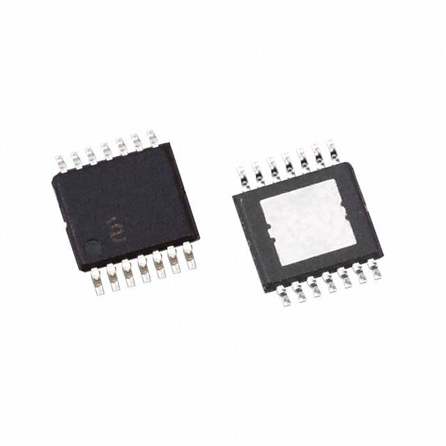


 工商网监
湘ICP备2023018690号
工商网监
湘ICP备2023018690号
