DATASHEET
SIGNS
FOR NEW DE
D
E
D
N
E
M
M
N OT R E C O
MENT PART
ED REPLACE
RECOMMEND
ISL80015IRZ-T
ISL8010
FN6191
Rev 6.00
October 18, 2010
Monolithic 600mA Step-Down Regulator with Low Quiescent Current
The ISL8010 is a synchronous, integrated FET 600mA
step-down regulator with internal compensation. It operates
with an input voltage range from 2.5V to 5.5V, which
accommodates supplies of 3.3V, 5V, or a Li-Ion battery
source. The output can be externally set from 0.8V to VIN
with a resistive divider.
The ISL8010 features automatic PFM/PWM mode control, or
PWM mode only. The PWM frequency is typically 1.4MHz
and can be synchronized up to 12MHz. The typical no load
quiescent current is only 120µA. Additional features include
a Power-Good output, 2.5V) forces the converter into
PWM mode in the next switching cycle regardless of output
current. The duration of the transition varies depending on the
output current. Figures 22 and 23 (under two different loading
conditions) show the device goes from PFM to PWM mode.
Note: In forced PWM mode, the IC will continue to start-up in
PFM mode to support pre-biased load applications.
Start-Up and Shutdown
When the EN pin is tied to VIN and VIN reaches
approximately 2.4V, the regulator begins to switch. The
inductor current limit is gradually increased to ensure proper
soft-start operation.
When the EN pin is connected to a logic low, the ISL8010 is
in the shutdown mode. All the control circuitry and both
MOSFETs are off, and VOUT falls to zero. In this mode, the
total input current is less than 1µA.
When the EN reaches logic HI, the regulator repeats the
start-up procedure, including the soft-start function.
Current Limit and Short-Circuit Protection
The current limit is set at about 1.2A for the PMOS. When a
short-circuit occurs in the load, the preset current limit restricts
the amount of current available to the output, which causes
the output voltage to drop as load demand increases. When
the output voltage drops 30mV below the reference voltage,
the converter will shutdown for a period of time (approximated
by Equation 1) and then restart. If the overcurrent condition
still exists, it will repeat the shutdown-wait-restart event. This
Page 9 of 11
�ISL8010
is called a “hiccup” event. The average power dissipation is
reduced, thereby reducing the likelihood of damaged current
and thermal conditions in the IC.
700 V IN
tHICCUP ---------------------------- + 216
3
(EQ. 1)
The inductor peak-to-peak ripple current is given as
Equation 4:
V IN – V O V O
I IL = -------------------------------------------L V IN f S
(EQ. 4)
L is the inductance
Thermal Shutdown
Once the junction reaches about +145°C, the regulator shuts
down. Both the P-Channel and the N-Channel MOSFETs
turn off. The output voltage will drop to zero. With the output
MOSFETs turned off, the regulator will cool down. Once the
junction temperature drops to about +130°C, the regulator
will perform a normal restart.
Thermal Performance
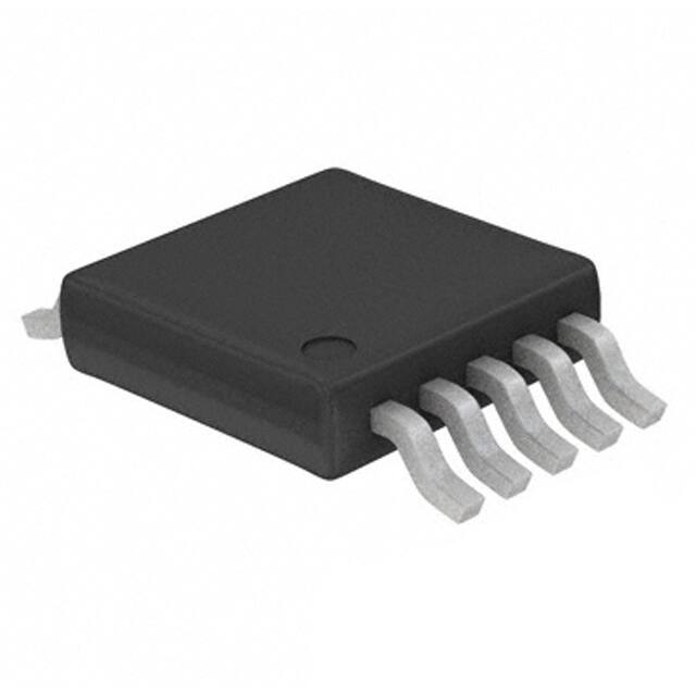
The ISL8010 is available in a fused-lead 10 Ld MSOP
package. Compared with regular 10 Ld MSOP package, the
fused-lead package provides lower thermal resistance. The
JA is +100°C/W on a 4-layer board and +125°C/W on
2-layer board. Maximizing the copper area around the pins
will further improve the thermal performance.
Power Good Output
The PG (pin 8) output is used to indicate when the output
voltage is properly regulating at the desired set point. It is an
open-drain output that should be tied to VIN or VCC through
a 100k resistor. If no faults are detected, EN is high, and
the output voltage is within ~5% of regulation, the PG pin will
be allowed to go high. Otherwise, the open-drain NMOS will
pull PG low.
Output Voltage Selection
Users can set the output voltage of the variable version with
a resistor divider, which can be chosen based on Equation 2:
R 1
V O = 0.8 1 + -------
R
2
(EQ. 2)
Because of the fixed internal compensation, the component
choice is relatively narrow. For a regulator with fixed output
voltage, only two capacitors and one inductor are required. It
is recommended to use between 10µF and 22µF multilayer
ceramic capacitors with X5R or X7R rating for both the input
and output capacitors, and 1.5µH to 2.2µH for the inductor.
The RMS current present at the input capacitor is decided by
Equation 3:
(EQ. 3)
This is about half of the output current IO for all the VO. This
input capacitor must be able to handle this current.
FN6191 Rev 6.00
October 18, 2010
The inductor must be able to handle IO for the RMS load
current, and to assure that the inductor is reliable, it must
handle the 2A surge current that can occur during a current
limit condition.
In addition to decoupling capacitors and inductor value, it is
important to properly size the phase-lead capacitor C4
(Refer to “Typical Application Diagram” on page 1). The
phase-lead capacitor creates additional phase margin in the
control loop by generating a zero and a pole in the transfer
function. As a general rule of thumb, C4 should be sized to
start the phase-lead at a frequency of ~2.5kHz. The zero will
always appear at lower frequency than the pole and follow
Equation 5:
1
f Z = ---------------------2R 2 C 4
(EQ. 5)
Over a normal range of R2 (~10kto 100k), C4 will range
from ~470pF to 4700pF. The pole frequency cannot be set
once the zero frequency is chosen as it is dictated by the
ratio of R1 and R2, which is solely determined by the desired
output set point. Equation 6 shows the pole frequency
relationship:
1
f P = --------------------------------------2 R 1 R 2 C 4
(EQ. 6)
Layout Considerations
The layout is very important for the converter to function
properly. The following PC layout guidelines should be
followed:
Component Selection
V O V IN – V O
I INRMS = ----------------------------------------------- I O
V IN
fS is the switching frequency (nominally 1.4MHz)
1. Separate the Power Ground ( ) and Signal Ground
( ); connect them only at one point right at the pins
2. Place the input capacitor as close to VIN and PGND pins
as possible
3. Make the following PC traces as small as possible:
- from LX pin to L
- from CO to PGND
4. If used, connect the trace from the FB pin to R1 and R2
as close as possible
5. Maximize the copper area around the PGND pin
6. Place several via holes under the chip to additional
ground plane to improve heat dissipation
The demo board is a good example of layout based on this
outline. Please refer to the ISL8010 Application Note.
Page 10 of 11
�ISL8010
Mini SO Package Family (MSOP)
0.25 M C A B
D
MINI SO PACKAGE FAMILY
(N/2)+1
N
E
MDP0043
A
E1
MILLIMETERS
PIN #1
I.D.
1
B
(N/2)
e
H
C
SEATING
PLANE
0.10 C
N LEADS
0.08 M C A B
b
SYMBOL
MSOP8
MSOP10
TOLERANCE
NOTES
A
1.10
1.10
Max.
-
A1
0.10
0.10
±0.05
-
A2
0.86
0.86
±0.09
-
b
0.33
0.23
+0.07/-0.08
-
c
0.18
0.18
±0.05
-
D
3.00
3.00
±0.10
1, 3
E
4.90
4.90
±0.15
-
E1
3.00
3.00
±0.10
2, 3
e
0.65
0.50
Basic
-
L
0.55
0.55
±0.15
-
L1
0.95
0.95
Basic
-
N
8
10
Reference
Rev. D 2/07
NOTES:
1. Plastic or metal protrusions of 0.15mm maximum per side are not
included.
L1
2. Plastic interlead protrusions of 0.25mm maximum per side are
not included.
A
3. Dimensions “D” and “E1” are measured at Datum Plane “H”.
4. Dimensioning and tolerancing per ASME Y14.5M-1994.
c
SEE DETAIL "X"
A2
GAUGE
PLANE
A1
L
0.25
3° ±3°
DETAIL X
© Copyright Intersil Americas LLC 2005-2010. All Rights Reserved.
All trademarks and registered trademarks are the property of their respective owners.
For additional products, see www.intersil.com/en/products.html
Intersil products are manufactured, assembled and tested utilizing ISO9001 quality systems as noted
in the quality certifications found at www.intersil.com/en/support/qualandreliability.html
Intersil products are sold by description only. Intersil may modify the circuit design and/or specifications of products at any time without notice, provided that such
modification does not, in Intersil's sole judgment, affect the form, fit or function of the product. Accordingly, the reader is cautioned to verify that datasheets are
current before placing orders. Information furnished by Intersil is believed to be accurate and reliable. However, no responsibility is assumed by Intersil or its
subsidiaries for its use; nor for any infringements of patents or other rights of third parties which may result from its use. No license is granted by implication or
otherwise under any patent or patent rights of Intersil or its subsidiaries.
For information regarding Intersil Corporation and its products, see www.intersil.com
FN6191 Rev 6.00
October 18, 2010
Page 11 of 11
�