DATASHEET
ISL8115
High Voltage Synchronous Buck PWM Controller with Integrated Gate Driver and
Current Sharing Capability
FN8272
Rev 1.00
September 23, 2013
Features
The ISL8115 is a synchronous buck PWM controller with
current sharing capability. The current sharing function allows
multiple modules to be connected in parallel to achieve higher
output current and to reduce input and output ripple current,
resulting in fewer components and reduced output dissipation.
• Wide VIN range operation: 2.97V to 36V; up to 5.5V output
and 30A load current per phase
• Fast transient response
- Voltage-mode PWM leading-edge modulation with
non-linear control
- Input voltage feed-forward
• Integrated 5V high speed 4A MOSFET gate drivers
- Internal bootstrap diode
• Excellent output voltage regulation
- 0.6V ±1.0% internal reference (-40°C ~ 125°C)
- 0.6V ±0.7% internal reference (-40°C ~ 105°C)
- Differential voltage sensing
• Excellent current balancing and overcurrent protection
- Peak and average overcurrent protection
- Output current monitor on the ISET pin
• Oscillator programmable from 150kHz to 1.5MHz
- Frequency synchronization to external clock signal
• Diode emulation mode for light load efficiency improvement
• Power-good open drain output
• Pre-bias start-up function
Utilizing voltage-mode control with input voltage feed-forward
compensation, the ISL8115 maintains a constant loop gain for
optimal transient response, especially for applications with a
wide input voltage range.
The ISL8115 protects against overcurrent conditions by
inhibiting the PWM operation while monitoring the current
with DCR of the output inductor, or a precision resistor. It also
has a pre-POR overvoltage protection option, which provides
some protection to the load if the upper MOSFET(s) is shorted.
The ISL8115 features remote ground sensing, programmable
input voltage UVLO, output under/overvoltage protection,
power-good indication, and fault Hand Shake capability.
Applications
• Power supply for datacom/telecom and POL
• Wide input voltage range buck regulators
• High current density power supplies RF power amplifier bias
compensation
• Output OVP, UVP; OTP
• Adjustable Soft-Start
ROS1
2k
ROS
2k
RFB3 3k
CFB3
3k
RFB3
RFB1
8.2nF 49.9Ω
C
CFB2
33nF
2.2nF
RFB2
787
13
VIN
11
RPCC 2*RJK0301
2*6TPF330M9L;
4*100µF; 4*1µ
5
COUT
2.2Ω
1
2
VOUT
1
2
3
10
R
2.8k
1
2
3
QL
4
9
8
7
CVIN1
4*10µF
4
CBOOT
QH
LOUT
320nH, 0.53mΩ, PA1513-321
1.5V/30A
0.22µF
2*RJK0305
VFF
CVIN 2.2µF
6
SS
RAMP
BOOT
12
5
ISENA
14
ISENB
15
VMON
16
RGND
17
CLKOUT
5
RFSET
24
UGATE
PGOOD
18.2k
PHASE
VCC
RSS
23
U1
ISL8115FRTZ
PLL_COMP
CONF
4
11.8k
22
PVCC
3
RCONF
CPVCC
4.7µF
LGATE
ISHARE
EN
21
FB
18
20
FSET
CPLL_H
390pF
25
GND
19
ISET
COMP
CISET
1nF
2
RPLL
5.11k
RISET
10k
1.27k
1
CPLL
2.2nF
0.22µF
RISEN
CFB1
RFF_H
CVCC
10k
2.2µF
REN_U
68.1k
RRAMP
113k
REN_L
140k
RFF_L
4.12k
33.2k
RVIN
2Ω
10V-15V
VIN
FIGURE 1. TYPICAL APPLICATION CIRCUIT, 10V-15V INPUT, 1.5V/30A OUTPUT
FN8272 Rev 1.00
September 23, 2013
Page 1 of 24
�ISL8115
Table of Contents
Application Diagrams . . . . . . . . . . . . . . . . . . . . . . . . . . . . . . . . . . . . . . . . . . . . . . . . . . . . . . . . . . . . . . . . . . . . . . . . . . . . . . . . . . . . . . . . 3
Block Diagram . . . . . . . . . . . . . . . . . . . . . . . . . . . . . . . . . . . . . . . . . . . . . . . . . . . . . . . . . . . . . . . . . . . . . . . . . . . . . . . . . . . . . . . . . . . . . . 5
Pin Configuration. . . . . . . . . . . . . . . . . . . . . . . . . . . . . . . . . . . . . . . . . . . . . . . . . . . . . . . . . . . . . . . . . . . . . . . . . . . . . . . . . . . . . . . . . . . . 6
Functional Pin Descriptions. . . . . . . . . . . . . . . . . . . . . . . . . . . . . . . . . . . . . . . . . . . . . . . . . . . . . . . . . . . . . . . . . . . . . . . . . . . . . . . . . . . 6
Ordering Information . . . . . . . . . . . . . . . . . . . . . . . . . . . . . . . . . . . . . . . . . . . . . . . . . . . . . . . . . . . . . . . . . . . . . . . . . . . . . . . . . . . . . . . . 7
Absolute Maximum Ratings . . . . . . . . . . . . . . . . . . . . . . . . . . . . . . . . . . . . . . . . . . . . . . . . . . . . . . . . . . . . . . . . . . . . . . . . . . . . . . . . . . . 8
Thermal Information . . . . . . . . . . . . . . . . . . . . . . . . . . . . . . . . . . . . . . . . . . . . . . . . . . . . . . . . . . . . . . . . . . . . . . . . . . . . . . . . . . . . . . . . . 8
Recommended Operating Conditions . . . . . . . . . . . . . . . . . . . . . . . . . . . . . . . . . . . . . . . . . . . . . . . . . . . . . . . . . . . . . . . . . . . . . . . . . . 8
Electrical Specifications . . . . . . . . . . . . . . . . . . . . . . . . . . . . . . . . . . . . . . . . . . . . . . . . . . . . . . . . . . . . . . . . . . . . . . . . . . . . . . . . . . . . . 8
Typical Performance Curves . . . . . . . . . . . . . . . . . . . . . . . . . . . . . . . . . . . . . . . . . . . . . . . . . . . . . . . . . . . . . . . . . . . . . . . . . . . . . . . . . 11
Functional Description . . . . . . . . . . . . . . . . . . . . . . . . . . . . . . . . . . . . . . . . . . . . . . . . . . . . . . . . . . . . . . . . . . . . . . . . . . . . . . . . . . . . . .
Functional Overview . . . . . . . . . . . . . . . . . . . . . . . . . . . . . . . . . . . . . . . . . . . . . . . . . . . . . . . . . . . . . . . . . . . . . . . . . . . . . . . . . . . . . . . . . . . . .
Initialization . . . . . . . . . . . . . . . . . . . . . . . . . . . . . . . . . . . . . . . . . . . . . . . . . . . . . . . . . . . . . . . . . . . . . . . . . . . . . . . . . . . . . . . . . . . . . . . . . . . .
Enable and Input Voltage UVLO . . . . . . . . . . . . . . . . . . . . . . . . . . . . . . . . . . . . . . . . . . . . . . . . . . . . . . . . . . . . . . . . . . . . . . . . . . . . . . . . . . . .
Pre-bias Startup . . . . . . . . . . . . . . . . . . . . . . . . . . . . . . . . . . . . . . . . . . . . . . . . . . . . . . . . . . . . . . . . . . . . . . . . . . . . . . . . . . . . . . . . . . . . . . . . .
Setting CONF Pin . . . . . . . . . . . . . . . . . . . . . . . . . . . . . . . . . . . . . . . . . . . . . . . . . . . . . . . . . . . . . . . . . . . . . . . . . . . . . . . . . . . . . . . . . . . . . . . .
Setting SS pin. . . . . . . . . . . . . . . . . . . . . . . . . . . . . . . . . . . . . . . . . . . . . . . . . . . . . . . . . . . . . . . . . . . . . . . . . . . . . . . . . . . . . . . . . . . . . . . . . . .
Frequency Setting . . . . . . . . . . . . . . . . . . . . . . . . . . . . . . . . . . . . . . . . . . . . . . . . . . . . . . . . . . . . . . . . . . . . . . . . . . . . . . . . . . . . . . . . . . . . . . .
Voltage Feed-forward . . . . . . . . . . . . . . . . . . . . . . . . . . . . . . . . . . . . . . . . . . . . . . . . . . . . . . . . . . . . . . . . . . . . . . . . . . . . . . . . . . . . . . . . . . . .
Non Linear Control. . . . . . . . . . . . . . . . . . . . . . . . . . . . . . . . . . . . . . . . . . . . . . . . . . . . . . . . . . . . . . . . . . . . . . . . . . . . . . . . . . . . . . . . . . . . . . .
Power-Good . . . . . . . . . . . . . . . . . . . . . . . . . . . . . . . . . . . . . . . . . . . . . . . . . . . . . . . . . . . . . . . . . . . . . . . . . . . . . . . . . . . . . . . . . . . . . . . . . . . .
Undervoltage and Overvoltage Protection . . . . . . . . . . . . . . . . . . . . . . . . . . . . . . . . . . . . . . . . . . . . . . . . . . . . . . . . . . . . . . . . . . . . . . . . . . .
POR Overvoltage Protection (POR-OVP) . . . . . . . . . . . . . . . . . . . . . . . . . . . . . . . . . . . . . . . . . . . . . . . . . . . . . . . . . . . . . . . . . . . . . . . . . . . . .
Over-Temperature Protection (OTP) . . . . . . . . . . . . . . . . . . . . . . . . . . . . . . . . . . . . . . . . . . . . . . . . . . . . . . . . . . . . . . . . . . . . . . . . . . . . . . . .
Inductor Current Sensing . . . . . . . . . . . . . . . . . . . . . . . . . . . . . . . . . . . . . . . . . . . . . . . . . . . . . . . . . . . . . . . . . . . . . . . . . . . . . . . . . . . . . . . . .
Peak Current Limit. . . . . . . . . . . . . . . . . . . . . . . . . . . . . . . . . . . . . . . . . . . . . . . . . . . . . . . . . . . . . . . . . . . . . . . . . . . . . . . . . . . . . . . . . . . . . . .
Average Overcurrent Protection. . . . . . . . . . . . . . . . . . . . . . . . . . . . . . . . . . . . . . . . . . . . . . . . . . . . . . . . . . . . . . . . . . . . . . . . . . . . . . . . . . . .
DEM . . . . . . . . . . . . . . . . . . . . . . . . . . . . . . . . . . . . . . . . . . . . . . . . . . . . . . . . . . . . . . . . . . . . . . . . . . . . . . . . . . . . . . . . . . . . . . . . . . . . . . . . . . .
Current Sharing . . . . . . . . . . . . . . . . . . . . . . . . . . . . . . . . . . . . . . . . . . . . . . . . . . . . . . . . . . . . . . . . . . . . . . . . . . . . . . . . . . . . . . . . . . . . . . . . .
Feedback Compensation . . . . . . . . . . . . . . . . . . . . . . . . . . . . . . . . . . . . . . . . . . . . . . . . . . . . . . . . . . . . . . . . . . . . . . . . . . . . . . . . . . . . . . . . .
Modulator Break Frequency Equations. . . . . . . . . . . . . . . . . . . . . . . . . . . . . . . . . . . . . . . . . . . . . . . . . . . . . . . . . . . . . . . . . . . . . . . . . . . . . .
Compensation Break Frequency Equations . . . . . . . . . . . . . . . . . . . . . . . . . . . . . . . . . . . . . . . . . . . . . . . . . . . . . . . . . . . . . . . . . . . . . . . . . .
14
14
14
14
14
14
14
15
15
15
15
16
16
16
16
17
18
18
18
19
20
20
Layout Considerations . . . . . . . . . . . . . . . . . . . . . . . . . . . . . . . . . . . . . . . . . . . . . . . . . . . . . . . . . . . . . . . . . . . . . . . . . . . . . . . . . . . . . . 21
General PowerPAD Design Considerations . . . . . . . . . . . . . . . . . . . . . . . . . . . . . . . . . . . . . . . . . . . . . . . . . . . . . . . . . . . . . . . . . . . . . . . . . . 22
Revision History. . . . . . . . . . . . . . . . . . . . . . . . . . . . . . . . . . . . . . . . . . . . . . . . . . . . . . . . . . . . . . . . . . . . . . . . . . . . . . . . . . . . . . . . . . . . 23
About Intersil . . . . . . . . . . . . . . . . . . . . . . . . . . . . . . . . . . . . . . . . . . . . . . . . . . . . . . . . . . . . . . . . . . . . . . . . . . . . . . . . . . . . . . . . . . . . . . 23
Package Outline Drawing . . . . . . . . . . . . . . . . . . . . . . . . . . . . . . . . . . . . . . . . . . . . . . . . . . . . . . . . . . . . . . . . . . . . . . . . . . . . . . . . . . . . 24
FN8272 Rev 1.00
September 23, 2013
Page 2 of 24
�ISL8115
Application Diagrams
ROS
2k
ROS1
2k
RFB3 14.7k
CFB3
14.7k
RFB3
3.3nF
RFB1
133Ω
CFB1
100pF
0.22µF
3k
CLKOUT
BOOT
VIN
R
7.15k
4
2*6TPF330M9L;
4*100µF; 4*1µF
COUT
RPCC
5
11
2.2Ω
1
1
2
3
10
9
8
CVIN1
4
CBOOT
0.22µF
7
QH
2
VOUT
LOUT
2.6ΩH, 1.58mΩ, 7443556260
5V/20A
2*10µF; 2*16SEPC270MX
BSC 03906NS
CVIN 2.2µF
VFF
SS
QL
1
2
3
13
ISEN A
14
ISEN B
VMON
15
16
RGND
17
FB
UGATE
12
6
RFSET
24
PHASE
CONF
RAMP
RSS
18.2k
23
PLL_COMP
5
11.8k
22
PVCC
U1
ISL8115FRTZ
PGOOD
RCONF
ISHARE
4
21
VCC
20
BSC 03906NS
CPVC C
4.7µF
LGATE
ISET
3
390pF
GND
EN
19
2
25
FSET
1nF
CPLL_H
COMP
CISET
1
RPLL
5.11k
RISET
10.5k
18
CPLL
2.2nF
5
RFB2
13k
C
RISEN
CFB2
4.7nF
RFF_H
CVCC
10k
2.2µF
RRAMP
113k
REN_L
140k
REN_U
174k
33.2k
RFF_L
3k
RVIN
2Ω
24V-36V
VIN
FIGURE 2. TYPICAL APPLICATION CIRCUIT, 24V-36V INPUT, 5V/20A OUTPUT
FN8272 Rev 1.00
September 23, 2013
Page 3 of 24
�ISL8115
Application Diagrams
ROS
2k
RFB3 3k
3k
RFB3
RFB1
8.2nF 49.9Ω
UGATE
BOOT
CLKOUT
1
2
3
2*6TPF330M9L; 4*100µF; 4*1µF
RPCC 2*RJK0301
5
9
7
COUT
2.2Ω
10
8
R
2.8k
1
4
CBOOT
VOUT
1.5V/2*30A
LOUT
320nH, 0.53mΩ, PA1513-321
4*10µF
QH
0.22µF
CVIN1
2
2*RJK0305
VFF
CVIN 2.2µF
6
1
RFSET
VIN
RAMP
FSET
SS
11
QL
4
1
2
3
ISENB
PHASE
U1
ISL8115FRTZ
12
5
14
RISEN
100Ω Rcsh
15
VMON
100pF Ccsh
16
17
CONF
5
24
18.2k
PLL_COMP
PGOOD
RFF_H
CVCC
113k
REN_L
2.2µF
10k
140k
REN_U
68.1k
33.2k
RFF_L
RSS
23
CPVCC
4.7µF
LGATE
RRAMP
11.8k
22
0.22µF
PVCC
EN
RCONF
1.27k
4
21
C
ISHARE
VCC
20
FB
25
GND
19
ISET
RGND
2.2nF
3
390pF
RFB2
787
18
CISET
1nF
CFB1
2
RPLL
5.11k
RISET
10k
33nF
COMP
CPLL
2.2nF
CPLL_H
CFB2
13
CFB3
ISENA
ROS1
2k
(Continued)
RVIN
4.12k
2Ω
10V-15V
VIN
ROS3
2k
RFB6 3k
3k
RFB5
RFB4
13
UGATE
BOOT
CVCC1
REN_L1
10k
2.2µF
REN_U1
68.1k
140k
VFF
VIN
1
2
3
5
2.2Ω
2
1
COUT1
10
R1
2.8k
4
RPCC1 2*RJK0301
2*6TPF330M9L;
4*100µF; 4*1µF
9
8
7
CVIN2
4*10µF
4
CBOOT1
QH1
LOUT1
320nH, 0.53mΩ,
PA1513-321
0.22µF
2*RJK0305
CVIN32.2µF
6
RAMP
SS
11
QL1
1
2
3
PHASE
U2
ISL8115FRTZ
12
5
14
RISEN1
100Ω Rcsh1
15
ISENB
FB
VMON
LGATE
CLKOUT
1
18.2k
24
PLL_COMP
CONF
CPVCC1
4.7µF
PVCC
5
RSS1
23
0.22µF
ISHARE
PGOOD
11.8k
22
1.27k
4
RCONF1
C1
RRAMP1
21
ISET
VCC
20
GND
EN
19
3
25
2
390pF
18
CISET1
1nF
COMP
10k
FSET
RPLL1
5.11k
RISET1
2.2nF
CPLL_H1
CPLL1
17
2.2nF
RFB7
787
RGND
CFB4
16
33nF
100pF Ccsh1
8.2nF 49.9Ω
CFB6
ISENA
CFB5
RFF_H1
RFF_L1
ROS2
2k
4.12k
33.2k
RVIN1
2Ω
FIGURE 3. 2-PHASE, 10V-15V INPUT, 1.5V/60A OUTPUT
FN8272 Rev 1.00
September 23, 2013
Page 4 of 24
�ISL8115
Block Diagram
2.2µF
4.7µF
2.2Ω
VCC
PVCC
11
3
VIN
7
1.22V
EN 2
INTERNAL SERIES
LINEAR REGULATOR
POWER-ON
RESET (POR)
OVER-TEMPERATURE
PROTECTION (OTP)
OV_H
CONTROLLER
SOFT-START
AND
FAULT LOGIC
OV_L
UV
OCP/UCP
9 UGATE
10kΩ
NON-LINEAR
CONTROL
VMON
DIGITAL
SOFT-START
8 BOOT
GATE
CONTROL
LOGIC
SAW
10 PHASE
SS-CODE
PVCC
E/A
FB 17
12 LGATE
PWM
RGND 16
Ish_corr1
40kΩ
DEM
8 CYCLE-BY-CYCLE
PEAK CURRENT
LIMIT
Ish_corr2
COMP 18
CURRENT
MIRROR
ISEN
OV_H
x1.20
1.135µA
13 ISENA
VMON 15
x1.15
x1.10
PGOOD 4
20µA
OV_L
OCP
UV
x0.50
x0.90
Vref
H
I
C
C
U
P
ISEN
ISEN
5xISEN + 50µA
OCP
14 ISENB
19
ISET
1.4V
UCP
20 ISHARE
0.25V
CISET
SAW
0.225V
MODE
SS-CODE
OSCILLATOR
DECODER
CURRENT
SHARE
BLOCK
Ish_corr1
GENERATOR
FN8272 Rev 1.00
September 23, 2013
24
22
5
6
21
1
23
EP
SS
CONF
RAMP
VFF
PLL_COMP
FSET
CLKOUT
GND
Ish_corr2
Page 5 of 24
�ISL8115
Pin Configuration
SS
CLKOUT
CONF
PLL_COMP
ISHARE
ISET
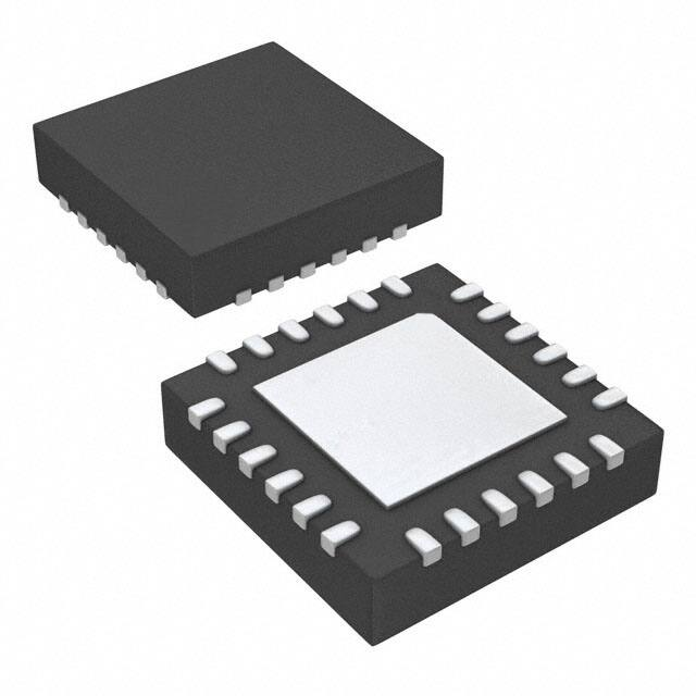
ISL8115 (24 LD 4x4 QFN)
TOP VIEW
24
23
22
21
20
19
FSET
1
18 COMP
EN
2
17
FB
VCC
3
16
RGND
15
VMON
GND
PGOOD
4
14 ISENB
RAMP 5
13
9
10
UGATE
PHASE
11
12
LGATE
8
PVCC
7
BOOT
6
VIN
VFF
ISENA
Functional Pin Descriptions
PIN
NUMBER
SYMBOL
1
FSET
Placing a resistor (RFSET) from this pin to GND to adjust the switching frequency.
Input an external clock signal to this pin and the internal oscillator synchronizes with the leading edge of the input signal.
2
EN
The input voltage to this pin is compared with a precision 1.22V reference. Tie this pin to ground to disable the part. Tie this
pin to VIN through a resistor divider to realize undervoltage lock-out.
3
VCC
This pin provides power for the analog circuitry. Connect this pin to a 2.97V to 5.15V bias through a recommended RC filter.
This pin can be powered up by the internal or external linear regulator. A 2.2µF filter capacitor is recommended to connect
closely to the pin.
4
PGOOD
Provides an open drain Power-Good signal when the voltage at VMON is within ±10% of nominal output regulation point after
soft-start is complete.
5
RAMP
A resistor to GND to set the sawtooth ramp. Select the resistor value to make the ramp amplitude the same as the voltage
on VFF. Refer to Voltage Feedforward Section on Page 15.
DESCRIPTION
T s – 275ns
1
R ramp = ----------------------------- ;Ts = -----------3 10pF
F SW
6
VFF
Pin for input voltage feed-forward. The voltage at this pin sets the internal oscillator ramp peak-to-peak amplitude at 1xVFF.
A resistor divider network from input voltage to this pin is required and an additional decoupling capacitor may be required
at this pin in noisy input environments. Make sure VFF is in the range of the clamp voltage (0.53V to 2.59V) specified in
“Electrical Specifications” on page 9.
7
VIN
This pin should be tied directly to the input rail when using the internal linear regulator. It provides power to the internal linear
drive circuitry.
8
BOOT
This pin provides the bootstrap bias for the high-side driver.
9
UGATE
This pin provides the drive signals for the high-side devices and should be connected to the high-side MOSFETs’ gates.
10
PHASE
Connect this pin to the source of the high-side MOSFETs and the drain of the low-side MOSFETs. This pin represents the return
path for the high-side gate drivers.
11
PVCC
Connect a 4.7µF capacitor closely to this pin. This pin is the output of the internal series linear regulator. It provides the bias
for both low-side and high-side drivers. Its operational voltage range is 2.97V to 5.3V. When the input supply is ≤5V, this pin
should be tied directly to VIN to eliminate the dropout voltage in the internal linear regulator.
FN8272 Rev 1.00
September 23, 2013
Page 6 of 24
�ISL8115
Functional Pin Descriptions (Continued)
PIN
NUMBER
SYMBOL
12
LGATE
This pin provides the drive for the low-side devices and should be connected to the lower MOSFETs’ gates.
13
ISENA
The positive input of the current sensing amplifier. Provide DCR, or precision resistor current sensing.
14
ISENB
The negative input of the current sensing amplifier. Provide DCR, or precision resistor current sensing.
15
VMON
This pin monitors the regulator’s output for OV and UV protection. PGOOD refers to the voltage on VMON. Connect a resistor
divider from VOUT to RGND, with the same ratio as the FB resistor divider. It is not recommended to share the resistor divider
for both FB and VMON; the response to a fault may not be as quick or robust. The voltage on this pin is also monitored for
the non-linear control.
16
RGND
Pin for remote ground sensing. There’s a current sourcing out from RGND if ISET voltage is lower than ISHARE in the
multi-phase configuration. A typical 100Ω resistor is required connected between RGND and negative terminal of the load.
17
FB
FB is the inverting input of the error amplifier. This pin is connected to the feedback resistor divider and provides the voltage
feedback signal for the controller.
18
COMP
This pin is the error amplifier’s output. It should be connected to the FB pin through a desired compensation network. The
lower limit of the voltage at COMP is 0.85V.
19
ISET
This pin sources a current equal to 5 times ISEN with 50µA offset. Connect RISET to the pin to adjust the OCP trigger point.
Parallel CISET with RISET to obtain the average output current signal at this pin. The voltage VISET set by an external resistor
RISET represents the sensed current for the controller which compares with the internal reference to implement over current
protection. Refer to the ““Average Overcurrent Protection” on page 18.
20
ISHARE
This pin is used for current sharing purpose and is configured to the current share bus representing all module’s reference
current. The voltage VISHARE represents the highest voltage of VISET of all active ISL8115(s) that connected together to the
current share bus. Float in single phase operation. Pulling this pin low will disable the ISL8115.
21
PLL_COMP
Compensation pin for the internal PLL circuit. A compensation network shows in the typical application diagram is required.
RPLL(5.11kΩ); CPLL(2.2nF); CPLL_H (390pF) are recommended.
22
CONF
A resistor at this pin is used to set: 1.) Enable or disable Diode emulation mode, and 2) Phase delay of clock out signal with
respect to input clock signal. See Table 1 for the resistor values.
23
CLKOUT
This pin provides clock signal to synchronize with other ISL8115(s). The phase delay of the CLKOUT with respect to the
external clock signal is configured through CONF pin.
24
SS
A resistor connected from this pin to ground is used to select the length of soft-start period. See Table 2 for the resistor
values.
25
GND
DESCRIPTION
All voltage levels are referenced to this pad. This pad provides a return path for the low side MOSFET drivers and internal
power circuitries as well as analog signals. Connect this pad to the board ground with the shortest possible path (9 vias to
the internal ground plane, placed on the soldering pad are recommended).
Ordering Information
PART NUMBER
(Notes 1, 2, 3)
PART MARKING
TEMP RANGE
(°C)
ISL8115FRTZ
81 15FRTZ
ISL8115EVAL1Z
12V to 1.5V/30A Evaluation Board
-40 to +125
ISL8115EVAL2Z
28V to 5V/20A Evaluation Board
PACKAGE
(Pb-free)
24 Ld Exposed Pad 4x4 TQFN
PKG.
DWG. #
L24.4x4F
NOTES:
1. Add “-T*” suffix for tape and reel. Please refer to TB347 for details on reel specifications.
2. These Intersil Pb-free plastic packaged products employ special Pb-free material sets, molding compounds/die attach materials, and 100% matte
tin plate plus anneal (e3 termination finish, which is RoHS compliant and compatible with both SnPb and Pb-free soldering operations). Intersil Pbfree products are MSL classified at Pb-free peak reflow temperatures that meet or exceed the Pb-free requirements of IPC/JEDEC J STD-020.
3. For Moisture Sensitivity Level (MSL), please see device information page for ISL8115. For more information on MSL please see techbrief TB363.
FN8272 Rev 1.00
September 23, 2013
Page 7 of 24
�ISL8115
Absolute Maximum Ratings
Thermal Information
VIN . . . . . . . . . . . . . . . . . . . . . . . . . . . . . . . . . . . . . . . . . . . . . . . . . -0.3V to 38V
PVCC. . . . . . . . . . . . . . . . . . . . . . . . . . . . . . . . . . . . . . . . . . . . . . . . -0.3V to +6V
VCC . . . . . . . . . . . . . . . . . . . . . . . . . . . . . . . . . . . . . . . . . . . . . . . . . -0.3V to +6V
PVCC to VCC . . . . . . . . . . . . . . . . . . . . . . . . . . . . . . . . . . . . . . . . . . .-1V to +1V
BOOT . . . . . . . . . . . . . . . . . . . . . . . . . . . . . . . . . . . . . . . . . . . . . . -0.3V to +44V
PHASE . . . . . . . . . . . . . . . . . . . . . . . . . . . . . . . . . . . . . . . . . . . . . -0.3V to +41V
PHASE Voltage Transient (20ns max) . . . . . . . . . . . . . . . . . . . . . . . GND - 2V
Boot to Phase Voltage, BOOT-PHASE . . . . . . . . . . . . . . . . . . . . . -0.3V to +6V
LGATE . . . . . . . . . . . . . . . . . . . . . . . . . . . . . . . . . . . . . . . . . . . . . . . -0.3V to +6V
LGATE Voltage Transient (20ns max) . . . . . . . . . . . . . . . . . . . . . . GND - 2.6V
ISENA, ISENB. . . . . . . . . . . . . . . . . . . . . . . . . . . . . . . . . . . . . -0.3V to +6.675V
Voltage on All Other Pins . . . . . . . . . . . . . . . . . . . . . . . . . -0.3V to VCC + 0.3V
ESD Rating
Human Body Model (Tested per JESD22-A114E) . . . . . . . . . . . . . . .2.5kV
Machine Model (Tested per JESD22-A115-A) . . . . . . . . . . . . . . . . . . 250V
Latch Up (Tested per JESD-78B; Class 1, Level A) . . . . . . . . . . . . . . 100mA
Thermal Resistance (Typical)
JA (°C/W) JC (°C/W)
24 Ld QFN Package (Note 5). . . . . . . . . . . .
39
3.5
Maximum Junction Temperature (Plastic Package) . . . . . . . . . . . .+150°C
Storage Temperature Range. . . . . . . . . . . . . . . . . . . . . . . .-65°C to +150°C
Pb-Free Reflow Profile . . . . . . . . . . . . . . . . . . . . . . . . . . . . . . . see link below
http://www.intersil.com/pbfree/Pb-FreeReflow.asp
Recommended Operating Conditions
Temperature . . . . . . . . . . . . . . . . . . . . . . . . . . . . . . . . . . . . .-40°C to +125°C
Input Voltage, VIN . . . . . . . . . . . . . . . . . . . . . . . . . . . . . . . . . . . . 2.97V to 36V
Driver Bias Voltage, PVCC . . . . . . . . . . . . . . . . . . . . . . . . . . . . . 2.97V to 5.5V
Signal Bias Voltage, VCC . . . . . . . . . . . . . . . . . . . . . . . . . . . . . . 2.97V to 5.5V
Boot-to-Phase Voltage (Overcharged), BOOT- PHASE. . . . . . . . . . . . . . . 9V
Input offset
Differential Current Sense Voltage
Range
ISET_OFFSET
IDEM_threshold
RISEN = 2kΩ
ISET Offset Current
ISEN Threshold of DEM
-0.2
6.375
V
-0.6
0.6
mV
-8
40
mV
44
50
55
µA
RISEN = 2kΩ
0.38
1.135
2.76
µA
VCC = 5.15V
17.6
20
22.4
OVERCURRENT PROTECTION
IOC
VISET_OC
ISEN Overcurrent Limit
ISET Pin OC Threshold
µA
VCC = 2.97V to 5.15V
20
µA
VCC = 2.97V to 5.15V
1.40
V
VCC = 5.15V
1.35
1.40
1.45
V
ISET Pin Under Current Threshold
0.22
0.25
0.28
V
ISHARE Pin Fault Threshold
0.22
0.225
0.24
V
0.2
V
ISHARE Pull-Down Voltage Capability
ISHARE = 500µA
POWER GOOD MONITOR AND UNDER/OVERVOLTAGE PROTECTION
VPG-
Power-Good Lower Threshold
Voltage from VMON to RGND; ~3 clock
cycles noise filter
0.51
0.54
0.57
V
VPG+
Power-Good Upper Threshold
Voltage from VMON to RGND; ~3 clock
cycles noise filter
0.63
0.66
0.69
V
PGOOD Low Output Voltage
IPGOOD = 2mA
0.35
V
UNDER/OVER VOLTAGE PROTECTION WITH VMON
VOV_NONLatch
Overvoltage Non-Latching Off
Threshold
Voltage from VMON to RGND; above the
Power-Good Upper Threshold
30
mV
Overvoltage Latching Off Threshold
Voltage from VMON to RGND; above the
OV Non-Latching UP Threshold
30
mV
Overvoltage LGATE Release Trip Point Voltage from VMON to RGND
0.51
V
VUV
Undervoltage Protection Trip Point
0.3
V
VUV
Undervoltage Protection Trip Point
Hysteresis
0.032
V
20
mV
Over-Temperature Protection Trip
Point
160
°C
OTP Release Threshold
145
°C
VOV_Latch
Voltage from VMON to RGND; after
soft-start completed
NON-LINEAR CONTROL
Offset of the non-linear control
Refer to Figure 23
OVER-TEMPERATURE PROTECTION
TOTP
NOTE:
7. Parameters with MIN and/or MAX limits are 100% tested at +25°C, unless otherwise specified. Temperature limits established by characterization
and are not production tested
FN8272 Rev 1.00
September 23, 2013
Page 10 of 24
�ISL8115
Typical Performance Curves
Unless otherwise stated, all curves were tested with example circuit in Figure 1.
95
95
90
90
CCM_VIN = 12V
EFFICIENCY (%)
EFFICIENCY (%)
CCM_VIN = 5V
85
80
75
85
80
75
FS = 220kHz
70
0
5
10
15
FS = 220kHz
70
20
0
5
OUTPUT CURRENT (A)
FIGURE 4. EFFICIENCY AT 12V INPUT, 1.5V OUTPUT
15
20
FIGURE 5. EFFICIENCY AT 5V INPUT, 1.5V OUTPUT
90
100
80
90
DEM_VIN = 5V
DEM_VIN = 12V
80
70
EFFICIENCY (%)
EFFICIENCY (%)
10
OUTPUT CURRENT (A)
CCM_VIN = 12V
60
50
CCM_VIN = 5V
70
60
50
40
40
FS = 220kHz
FS = 220kHz
30
0.5
1.5
2.5
30
3.5
0.5
1.5
OUTPUT CURRENT (A)
2.5
3.5
OUTPUT CURRENT (A)
FIGURE 6. EFFICIENCY vs LOAD CURRENT AT 12V INPUT
FIGURE 7. EFFICIENCY vs LOAD CURRENT AT 5V INPUT
0.00000
-0.010
OUTPUT VOLTAGE (%)
OUTPUT VOLTAGE (%)
-0.00010
-0.012
-0.014
-0.016
-0.018
-0.00020
-0.00030
-0.00040
-0.00050
-0.00060
-0.00070
-0.020
10
12
14
INPUT VOLTAGE (V)
FIGURE 8. LINE REGULATION, VOUT = 1.5V, IO = 20A
FN8272 Rev 1.00
September 23, 2013
16
-0.00080
0
5
10
15
20
25
30
OUTPUT CURRENT (A)
FIGURE 9. LOAD REGULATION, VIN = 12V, VOUT = 1.5V
Page 11 of 24
35
�ISL8115
Typical Performance Curves
Unless otherwise stated, all curves were tested with example circuit in Figure 1. (Continued)
EN: 500mV/DIV
VOUT : 500mV/DIV
IOUT : 10A/DIV
COMP: 500mV/DIV
EN: 500mV/DIV
VOUT : 500mV/DIV
PHASE: 5V/DIV
ss: 500mV/DIV
5ms/DIV
FIGURE 10. FULL LOAD START-UP
FIGURE 11. PRE-BIAS START-UP
VOUT : 1V/DIV
VOUT : 50mV/DIV (AC)
IOUT : 20A/DIV
IOUT : 10A/DIV
PHASE: 10V/DIV
20µs/DIV
10ms/DIV
FIGURE 12. HICCUP OCP
FIGURE 13. TRANSIENT RESPONSE 2A/µs
IL1: 4A/DIV
IL2: 4A/DIV
VOUT : 50mV/DIV (AC)
IOUT : 10A/DIV
ISET1: 200mV/DIV
ISET2: 200mV/DIV
20µs/DIV
FIGURE 14. TRANSIENT RESPONSE 2A/µs
FN8272 Rev 1.00
September 23, 2013
FIGURE 15. CURRENT SHARING WITH 2-PHASE CONFIGURATION
Page 12 of 24
�ISL8115
Typical Performance Curves
Unless otherwise stated, all curves were tested with example circuit in Figure 1. (Continued)
17.50
21.55
17.45
21.50
21.45
17.35
VIN = 24V
21.40
IOC (µA)
IQ_VIN_DISABLE (µA)
17.40
17.30
17.25
21.35
21.30
17.20
21.25
17.15
21.20
17.10
17.05
-50
-25
0
25
50
75
100
21.15
-50
125
-25
0
TEMPERATURE (°C)
25
50
75
100
125
TEMPERATURE (°C)
FIGURE 16. SHUTDOWN CURRENT vs TEMPERATURE
FIGURE 17. OVERCURRENT THRESHOLD vs TEMPERATURE
45
0.6005
40
0.6000
35
3.3V INPUT
0.5995
TD (ns)
VREF (V)
30
0.5990
25
12V INPUT
20
15
10
0.5985
5
0.5980
-50
-25
0
25
50
75
100
0
-50
125
-25
0
TEMPERATURE (°C)
50
75
100
125
1350
1550
FIGURE 19. DEAD TIME vs TEMPERATURE
499.60
190
499.40
170
499.20
150
499.00
130
RFSET (kΩ)
FREQUENCY (kHz)
FIGURE 18. FEEDBACK VOLTAGE REFERENCE vs TEMPERATURE
498.80
498.60
25
TEMPERATURE (°C)
RFSET = 47.8k
498.40
110
90
70
498.20
50
498.00
30
497.80
497.60
-50
-25
0
25
50
75
TEMPERATURE (°C)
FIGURE 20. FREQUENCY vs TEMPERATURE
FN8272 Rev 1.00
September 23, 2013
100
125
10
150
350
550
750
950
1150
FREQUENCY (kHz)
FIGURE 21. FREQUENCY vs RFSET
Page 13 of 24
�ISL8115
Functional Description
Functional Overview
The ISL8115 is a synchronous buck PWM controller with current
sharing capability. The current sharing function allows multiple
modules to be connected in parallel to achieve higher output
current. The controller also features multi-phase operation to reduce
input and output ripple current, resulting in fewer components and
reduced output dissipation.
Utilizing voltage-mode control with input voltage feed-forward
compensation, the ISL8115 maintains a constant loop gain for
optimal transient response, especially for applications with a wide
input voltage range.
Initialization
The ISL8115 requires VCC and PVCC biased by a single supply.
The Power-On Reset (POR) function continually monitors the
input supply voltages (PVCC and VCC) and the voltage at EN pin.
With PVCC, VCC and EN above their POR thresholds, the IC will
initialize a process to read the resistor value on the CONF and SS
pins. This process can take up to 2ms. Failure to read the resistor
values will stop the soft-start process.
Use a resistor with 1% tolerance on the CONF pin.
TABLE 1. RESISTOR VALUES TO SET CONF PIN
PHASE DELAY
(°)
DEM
1% TOLERANCE RESISTOR
VALUE (kΩ)
0
ENABLE
46.4
60
73.2
90
105
120
137
180
11.8
240
18.2
270
26.1
300
34
0
60
DISABLE
(Force CCM)
2.94
4.53
90
6.49
120
8.66
180
0.732
After successfully reading the resistor values on the CONF and SS
pins, there is another 1ms delay for the PLL.
240
1.13
270
1.62
If the system voltage drops below the falling POR threshold, then
UGATE and LGATE are forced off. Also ISHARE is pulled low.
300
2.15
Enable and Input Voltage UVLO
Setting SS pin
When the voltage on EN pin is greater than the 1.22V threshold,
the controller is enabled. If the EN voltage is less than 1.22V
minus the hysteresis (typical 65mV), the controller is disabled.
A resistor connected from the SS pin to ground is used to set the
length of the output soft-start time. The internal soft-start DAC
operates with and internal 2MHz clock. The value of the resistor
on this pin set number on steps for the soft-start. The resistor
value and the corresponding soft-start duration is shown in
Table 2. Use a resistor with 1% tolerance on the SS pin.
The EN pin can be used as a voltage monitor for the input
undervoltage lock-out by connecting the EN pin to the input rail
through a resistor divider.
Pre-bias Startup
TABLE 2. RESISTOR VALUES TO SET SOFT-START TIME
1% TOLERANCE
RESISTOR VALUE
(kΩ)
SOFT-START TIME
(ms)
46.4
0.4
73.2
0.8
105
1.2
Setting CONF Pin
137
2.2
A resistor connected from the CONF pin to ground is used to:
11.8
4.8
• Enable or disable diode emulation mode (DEM) after soft-start.
18.2
8.8
• Set the phase delay of CLKOUT with respect to an external
clock signal applied to the FSET pin.
26.1
12.8
34
25.6
A pre-bias voltage may exist at the output before the controller is
enabled. The ISL8115 can support a pre-bias startup condition
by keeping UGATE and LGATE off until the internal soft-start
voltage exceeds the feedback voltage. This feature prevents the
output voltage from discharging through the lower MOSFET
during the soft-start.
When using multiple ISL8115s in parallel module configuration,
all soft-start times must be set to the same value.
FN8272 Rev 1.00
September 23, 2013
Page 14 of 24
�ISL8115
Frequency Setting
The peak-to-peak amplitude of the sawtooth yields as:
The switching frequency is set by the RFSET connected between
the FSET pin and ground. Figure 21 shows the typical RFSET vs
Frequency variation curve. Equation 1 illustrates the relationship
between RFSET and switching frequency.
To synchronize with an external clock, apply a clock signal in the
programmable oscillator range of 150kHz to 1.5MHz to the FSET
pin. A duty cycle in the range of 10% to 90% is required.
·
9
–9
1
R FSET = 25 10 ----------- – 85 10
Fsw
(EQ. 1)
T s – 275ns
V ramp – pk – pk = I disch arg e ----------------------------10pF
(EQ. 2)
where:
V FF
I disch arg e = --------------------3R ramp
(EQ. 3)
1
T s = ---------F sw
According to the Equations 2 and 3, design the resistor at the
RAMP pin to make the amplitude of sawtooth equal to VFF.
Voltage Feed-forward
T s – 275ns
R ramp = ----------------------------3 10pF
The voltage applied to the VFF pin can adjust the amplitude of
the internal sawtooth ramp. It is recommended to set the
amplitude equal to VFF. This helps to maintain a constant gain
contributed by the modulator and the input voltage to achieve
optimum loop response over a wide input voltage range.
Figure 22 shows the feed-forward circuits.
For example, select 113kΩ for RFSET to achieve 220kHz
switching frequency and 140kΩ for Rramp to make the
Vramp_pk_pk = VFF. The sawtooth ramp offset voltage is 1V and
the peak of the sawtooth is to VFF +1V.
Fsw
Vin
Vramp_peak
Vcc-2.2V
+
3xI_discharge
1V
VFF
Vramp_pk_pk
Ideal
diode
+
10pF
I_discharge
(EQ. 4)
Non Linear Control
In order to respond faster to a load step, non-linear control has
been introduced in ISL8115. If the feedback voltage at VMON is
greater than the voltage of the previous cycle plus 20mV
(typical), the LG turns on immediately without waiting for the next
clock signal. This function helps to improve the transient
response especially for a controller with leading-edge modulator.
-
Fsw
20mV
+
-
+
-
-
Ideal
diode
+
Turn on
LG
0.5V
RAMP
Rramp
VMON
FIGURE 23. NON-LINEAR CONTROL CIRCUIT
Vramp_peak
Vramp_pk_pk
275ns
Ts
FIGURE 22. FEED-FORWARD CIRCUITRY
VFF voltage is clamped between 0.5V (typical) and VCC-2.2V
(typical). To make the feed forward work for all input voltage, the
voltage on VFF pin should be designed within this range.
Power-Good
The Power-Good comparator monitors the voltage on the VMON
pin. The trip points are shown in Figure 24. Power-Good will not
be asserted until the completion of the soft-start cycle. The
Power-Good pulls low when EN is low or VMON is out of the
threshold window. PGOOD stays high until the fault exists for
three consecutive clock cycles.
VREF
END OF SS
PGOOD
x1.10
VMON
x0.90
3 Clock
Cycles Filter
OC, OC, UV AND OT
FIGURE 24. PGOOD CIRCUIT
FN8272 Rev 1.00
September 23, 2013
Page 15 of 24
�ISL8115
Undervoltage and Overvoltage Protection
Inductor Current Sensing
The Undervoltage (UV) and Overvoltage (OV) protection circuitry
monitors the voltage on the VMON pin.
The ISL8115 supports inductor DCR sensing techniques up to
5.5V output voltage, as shown in Figure 25.
An OV event (VOUT > 120%) causes the high-side MOSFET to latch
off permanently, while the low-side MOSFET turns on and then
turns off after the output voltage drops below 85%. At the same
time, the PGOOD and ISHARE are also latched low. The latch
condition can be reset only by re-cycling VCC or EN.
I s
L
UGATE
L
PHASE
ISL8115
INTERNAL CIRCUIT
VL
COUT
+ VC(s) R
C
RISEN
CURRENT
MIRROR
+
I SET
VOUT
DCR
INDUCTOR
LGATE
+
ISL8115 has 2 level OV thresholds: 115% (non-latch), and 120%
(Latch). In an OV event with VMON between 115% and 120%, the
high-side MOSFET is turned off, while the low-side MOSFET turns
on. At the same time PGOOD is also pulled down. When the
VMON voltage drops to 85% of reference voltage, the LGATE is
turned off, then hiccup restart occurs.
VIN
-
The UV functionality is not enabled until the end of soft-start. If
the VMON drops below 50% of the 0.6V internal reference, the
controller goes into hiccup mode and recovers until VMON rises
up to 0.332V.
-
ISENA
ISENB
POR Overvoltage Protection (POR-OVP)
When both the VCC and PVCC are below the POR thresholds, the
UGATE is low and LGATE is floating (high impedance). EN has no
control over LGATE when below POR. When above POR, the
LGATE will toggle with its PWM pulses. An external 10kΩ resistor
can be placed between the PHASE and LGATE node to implement
a PRE-POR-OVP circuit. The output of the converter is equal to the
phase node voltage via output inductor and then is effectively
clamped to the low-side MOSFET’s gate threshold voltage, which
provides some protection to the load if the upper MOSFET(s) is
shorted during start-up, shutdown, or normal operations. For
complete protection, the low-side MOSFET should have a gate
threshold that is much smaller than the maximum voltage rating
of the load.
The PRE-POR-OVP works against pre-biased start-up when
pre-charged output voltage is higher than the threshold of the
low-side MOSFET.
Over-Temperature Protection (OTP)
When the junction temperature of the IC is greater than +160°C
(typically), the Ugate and Lgate are forced off. The ISHARE and
PGOOD pins are forced low indicating a fault. In a multi-phase
configuration, this pulls the ISHARE bus low and informs other
channels to turn off. All connected ISHARE pins stay low, but
release after the IC’s junction temperature drops below the
+15°C hysteresis (typical). The device now starts the
initialization process of reading the CONFIG and SS resistors, PLL
locking, and soft-start.
FN8272 Rev 1.00
September 23, 2013
ISEN
FIGURE 25. DCR SENSING CONFIGURATION
An inductor’s winding is characteristic of a distributed resistance
as measured by the DCR (Direct Current Resistance) parameter.
Consider the inductor DCR as a separate lumped quantity, as
shown in Figure 25. The inductor current, IL, will also pass
through the DCR. Equation 5 shows the S-domain equivalent
voltage across the inductor VL.
V L = I L s L + DCR
(EQ. 5)
A simple R-C network across the inductor extracts the DCR
voltage, as shown in Figure 25. The voltage on the capacitor VC,
can be shown to be proportional to the inductor current IL, see
Equation 6.
L
s ------------+ 1 DCR I L
DCR
V C = -------------------------------------------------------------------- s RC + 1
(EQ. 6)
If the R-C network components are selected such that the RC
time constant (= R*C) matches the inductor time constant
(= L/DCR), the voltage across the capacitor VC is equal to the
voltage drop across the DCR, i.e., proportional to the inductor
current. The value of R should be as small as feasible for best
signal-to-noise ratio. Make sure the resistor package size is
appropriate for the power dissipated and include this loss in
efficiency calculations.
Page 16 of 24
�ISL8115
In calculating the minimum value of R, the average voltage
across C (average of ILDCR product) is small and can be
neglected. Therefore, the minimum value of R may be
approximated Equation 7:,
2
2
D V IN – max – V OUT + 1 – D V OUT
R min = ------------------------------------------------------------------------------------------------------------k P R – pkg P
With the internal low-offset current amplifier, the capacitor
voltage Vc is replicated across the sense resistor RISEN.
Therefore, the current out of ISENB pin, ISEN, is proportional to
the inductor current.
(EQ. 7)
Peak Current Limit
The ISL8115 contains a peak current limit circuit to protect the
converter.
where PR-pkg is the maximum power dissipation specification for
the resistor package and P is the derating factor for the same
parameter (e.g., PR-pkg = 0.063W for 0402 package, P = 80% @
+85°C). k is the margin factor, also to limit temperature raise in
the resistor package, recommend using 0.4. Once Rmin has been
calculated, solve for the maximum value of C from Equation 8:
L
C max = -------------------------------R min DCR
When a peak current limit occurs, the UG is turned off
immediately. An internal counter begins to record the number of
OC events detected. Two consecutive clock cycles without a
current limit will reset the counter. If 8 consecutive clock cycles
of overcurrent is detected, the ISL8115 enters into a hiccup
mode. The ISL8115 operation during the peak current limit event
is illustrated in Figure 26.
(EQ. 8)
The sensed current signal and peak current signal in Figure 25
can be derived by the following equations:
Next, choose the next-lowest readily available value. Then
substitute the chosen value into the same equation and
re-calculate the value of R. Choose a 1% resistor standard value
closest to this re-calculated value of R. For example, when VINMax = 14.4V, VOUT = 2.5V, L = 1mH and DCR = 1.5mΩ, with 0402
package Equation 7 yields Rmin of 1476Ω and Equation 8 yields
Cmax of 0.45µF. Choose 0.39µF and re-calculate, the resistor
yields 1.69k.
I L DCR
I SEN = ----------------------R ISEN
(EQ. 9)
V out 1 – D
I L + ------------ -------------- DCR
L
2F sw
I SEN – PK = -----------------------------------------------------------------R ISEN
(EQ. 10)
UG OFF
CURRENT LIMIT
20µA (TYPICAL)
1
2
3
1
2
3
ISEN
No trigger in two consecutive
cycles will reset the counter
4
5
6
7
8
0A
HICCUP
PHASE
CLOCK
FIGURE 26. CURRENT LIMIT TIMING
FN8272 Rev 1.00
September 23, 2013
Page 17 of 24
�ISL8115
Average Overcurrent Protection
DEM
The ISL8115 provides an average overcurrent protection circuit
to protect the converter during an overcurrent fault.
Diode emulation allows for higher converter efficiency under light
load situations. With diode emulation active, the ISL8115 will
detect the zero current crossing of the output inductor and turn
off LGATE. This ensures that discontinuous conduction mode
(DCM) is achieved. This prevents the low side MOSFET from
sinking current and discharging of the output during pre-biased
startup. DEM can only be disabled after soft-start. Please refer to
the “Electrical Specifications” table on page 10 for the threshold
of DEM.
The voltage on pin ISET represents the average inductor current
signal which compares with an internal reference of 1.4V to
implement positive overcurrent protection and 0.25V for
negative current protection. If the overcurrent event is detected,
the ISL8115 will enter hiccup mode. This consists of a 10ms shut
down and then a restart. The voltage on pin ISET can be obtained
from Equation 11. The circuit of average OCP is shown in
Figure 27.
(EQ. 11)
V ISET = 5I SEN + 50A R ISET
5
1.4V
50µA
Isen
5xIsen
+
-
OC
HICCUP
0.25V
+
-
ISET
+
MULTIPLIER
Current Sharing
The ISL8115 can support up to 6 phase operation. Connecting
the ISHARE pins together allows for communication between the
phases. In a single phase application, the voltage on the ISHARE
pin follows the ISET voltage and the ISHARE pin can be floated.
However, in multi-phase applications, the voltage on the ISHARE
bus represents the highest ISET voltage of all phases. This
voltage becomes the current reference of each phase. Figure 28
illustrates the relation between ISHARE and ISET.
PHASE
RISET
VOUT
CISET
`
+ Vc RISEN
ISENB
CSA
ISEN
FIGURE 27. AVERAGE OCP CIRCUIT
-
ISENA
Select a suitable RISET for setting the OCP trigger point. Also, a
filer capacitor CISET is required in parallel with RISET to get the
average inductor current signal.
ISEN = Vc
RISEN
V`
Iset
=ILxDCR
RISEN
ISET
1
I
+ --- di DCR
(EQ. 12)
OC 2
24A + 4A 1.6m
R SEN = ------------------------------------------------- = ------------------------------------------------------- = 2.24k
20uA
20uA
Considering DCR increases as the temperature rises. Select 3kΩ
(2.24kΩ x 1.34) for RSEN.
The voltage difference between ISHARE and ISET will create two
correction currents (See Figure 29). One is Ish_corr1 which
makes the COMP voltage increase and the other is Ish_corr2
which makes the RGND voltage increase. A resistor (typically
100Ω) connected between RGND and the output capacitor
ground is required. The correction currents make the duty cycle
increase thereby making the voltage at ISET track the voltage at
ISHARE within 10mV of offset.
COMP
10mV
(EQ. 13)
+
-
+
gm
Ish_corr1
+
Gain1
-
To filter the inductor ripple current and achieve the average
inductor current signal from ISET, the roll off frequency of the low
pass filter should be much lower than the switching frequency.
Capacitor at ISET CISET is obtained by Equation 14:
1
1
---------------------------------------------- ------ F SW
2R ISET C ISET 10
1
10
C ISET ------------ ------------------------- = 0.68nF
F SW 2R ISET
ISHARE BUS
FIGURE 28. CURRENT SENSING BLOCK DIAGRAM
To set 22A for the average OCP, the value of RISET can be yield
as:
1.4V
R ISET = -------------------------------------------------------------------------- = 10.7k
22A 1.34DCR
------------------------------------------- 5 + 50uA
3k
ISHARE
RISET
Generally, set the average OCP trigger point lower than the peak
current limit.
For example, L = 2.5µH; DCR = 1.6mΩ; IOUT = 20A; di = 8A;
FSW = 220kHz. To set 24A as the output peak current limit. RSEN
can be derived by:
+
V`
Gain2
Ish_corr2
ISHARE
(EQ. 14)
ISET
RGND
FIGURE 29. CURRENT SHARING BLOCK DIAGRAM
Select a 1nF Capacitor for CISET.
FN8272 Rev 1.00
September 23, 2013
Page 18 of 24
�ISL8115
Vin
EN
ISHARE CLKOUT
EN
FSET
Module1
ISL8115
RGND
Rcsr
100ohm
ISHARE
EN
FSET
Module2
ISL8115
FSET
RFSET
RGND
ISHARE
Module3
ISL8115
CLKOUT
CLKOUT
RGND
Rcsr
100ohm
RISHARE
40kohm
Rcsr
100ohm
FIGURE 30. SIMPLIFIED MULTI-PHASE DIAGRAM
Figure 30 shows 3-phase operation. Device 1 is the master and
the remaining devices are synchronized and phase shifted. The
phase shift can be set using the CONF pin.
VIN
DRIVER
OSC
PWM COMPARATOR
VOSC
The ISHARE bus remains low until the PLL of all phases are
locked. This assures that all phases start up at the same time,
thereby preventing an overcurrent condition. A 40kΩ resistor is
required between the ISHARE bus and ground.
Lo
_
PHASE
+
Vo
DRIVER
Co
ESR
Feedback Compensation
ZFB
ZIN
_
VCOMP
+
Figure 31 highlights the voltage-mode control loop for a
synchronous-rectified buck converter. The output voltage (VOUT)
is regulated to the reference voltage level. The error amplifier
output (VEA) is compared with the oscillator (OSC) sawtooth
waveform to provide a pulse-width modulated (PWM) signal with
an amplitude of VIN at the PHASE node. The PWM signal is
smoothed by the output filter (LO and CO).
REFERENCE
ERROR AMP
DETAILED COMPENSATION
COMPONENTS
This function is dominated by a DC Gain and the output filter (LO
and CO), with a double pole break frequency at FLC and a zero at
FESR. The DC Gain of the modulator is simply the input voltage
(VIN) divided by the peak-to-peak oscillator voltage VOSC.
ZFB
C2
Vo
ZIN
C1
R2
R3
C3
R1
VCOMP
FB
_
+
ISL8115
R4
REFERENCE
VOUT VREF*(1+R1/R4)
FIGURE 31. VOLTAGE- MODE BUCK CONVERTER COMPENSATION
DESIGN
FN8272 Rev 1.00
September 23, 2013
Page 19 of 24
�ISL8115
Modulator Break Frequency Equations
1
F LC = --------------------------------------2 L O C O
100
(EQ. 15)
FZ1 FZ2
FP1
FP2
80
OPEN LOOP
ERROR AMP GAIN
1
F ESR = --------------------------------------------2 ESR C O
(EQ. 16)
The compensation network consists of the error amplifier
(internal to the ISL8115) and the impedance networks ZIN and
ZFB. The goal of the compensation network is to provide a closed
loop transfer function with the highest 0dB crossing frequency
(f0dB) and adequate phase margin. Phase margin is the
difference between the closed loop phase at f0dB and 180°. The
following equations relate to the compensation network’s poles,
zeros and gain to the components (R1, R2, R3, C1, C2, and C3) in
Figure 31. Use the following guidelines for locating the poles and
zeros of the compensation network.
Compensation Break Frequency Equations
1
F Z1 = ---------------------------------2 R 2 C1
(EQ. 17)
1
F P1 = ------------------------------------------------------C1 C2
2 R2 ----------------------
C1 + C2
(EQ. 18)
1
F Z2 = -----------------------------------------------------2 R1 + R3 C3
(EQ. 19)
1
F P2 = ---------------------------------2 R3 C3
(EQ. 20)
40
20
20LOG
(R2/R1)
20LOG
(VIN/DVOSC)
0
COMPENSATION
GAIN
MODULATOR
GAIN
-20
LOOP GAIN
-40
-60
FLC
10
100
1k
FESR
10k
100k
1M
10M
FREQUENCY (Hz)
FIGURE 32. ASYMPTOTIC BODE PLOT OF CONVERTER GAIN
The compensation gain uses external impedance networks ZFB
and ZIN to provide a stable, high bandwidth (BW) overall loop. A
stable control loop has a gain crossing with -20dB/decade slope
and a phase margin greater than 45°. Include worst case
component variations when determining phase margin.
Component Selection Guidelines
OUTPUT CAPACITOR SELECTION
1. Pick Gain (R2/R1) for desired converter bandwidth
2. Place 1ST Zero Below Filter’s Double Pole (~75% FLC)
3. Place 2ND Zero at Filter’s Double Pole
4. Place 1ST Pole at the ESR Zero
5. Place 2ND Pole at Half the Switching Frequency
6. Check Gain against Error Amplifier’s Open-Loop Gain
7. Estimate Phase Margin - Repeat if Necessary
Figure 32 shows an asymptotic plot of the DC/DC converter’s
gain vs frequency. The actual Modulator Gain has a high gain peak
due to the high Q factor of the output filter and is not shown in
Figure 32. Using the previously mentioned guidelines should give a
compensation gain similar to the curve plotted. The open loop
error amplifier gain bounds the compensation gain. Check the
compensation gain at FP2 with the capabilities of the error
amplifier. The Loop Gain is constructed on the log-log graph of
Figure 32 by adding the Modulator Gain (in dB) to the
Compensation Gain (in dB). This is equivalent to multiplying the
modulator transfer function to the compensation transfer function
and plotting the gain.
FN8272 Rev 1.00
September 23, 2013
GAIN (dB)
60
The output capacitors should be selected to meet the dynamic
regulation requirements including ripple voltage and load
transients. Selection of output capacitors is also dependent on
the output inductor, thus some inductor analysis is required to
select the output capacitors.
One of the parameters limiting the converter’s response to a load
transient is the time required for the inductor current to slew to
its new level. The response time is the time interval required to
slew the inductor current from an initial current value to the load
current level. During this interval the difference between the
inductor current and the transient current level must be supplied
by the output capacitor(s). Minimizing the response time can
minimize the output capacitance required. Also, if the load
transient rise time is slower than the inductor response time, as
in a hard drive or CD drive, it reduces the requirement on the
output capacitor.
The maximum capacitor value required to provide the full, rising
step, transient load current during the response time of the
inductor is shown in Equation 21:
2
L O I TRAN
C OUT = ----------------------------------------------------------2 V IN – V O DV OUT
(EQ. 21)
where COUT is the output capacitor(s) required, LO is the output
inductor, ITRAN is the transient load current step, VIN is the input
voltage, VO is output voltage, and DVOUT is the drop in output
voltage allowed during the load transient.
Page 20 of 24
�ISL8115
High frequency capacitors initially supply the transient current
and slow the load rate-of-change seen by the bulk capacitors. The
bulk filter capacitor values are generally determined by the ESR
(Equivalent Series Resistance) and voltage rating requirements
as well as actual capacitance requirements.
The output voltage ripple is due to the inductor ripple current and
the ESR of the output capacitors as defined by Equation 22:
V RIPPLE = I L ESR
(EQ. 22)
High frequency decoupling capacitors should be placed as close
to the power pins of the load as physically possible. Be careful
not to add inductance in the circuit board wiring that could
cancel the usefulness of these low inductance components.
Consult with the manufacturer of the load circuitry for specific
decoupling requirements.
Use only specialized low-ESR capacitors intended for
switching-regulator applications for the bulk capacitors. In most
cases, multiple small-case electrolytic capacitors perform better
than a single large-case capacitor.
MOSFET SELECTION
The logic level MOSFETs are chosen for optimum efficiency given
the potentially wide input voltage range and output power
requirements, two N-Channel MOSFETs for the Buck converter.
These MOSFETs should be selected based upon rDS(ON), gate
supply requirements, and thermal management considerations.
Compared with other components, MOSFETs contribute
significant power loss to the converter. Power loss of high side
FET includes switching losses, conduction losses and gate charge
losses. Low side FET contributes conduction losses and gate
charge losses too, also reverse recovery loss and loss of the body
diode during dead time should be considered.
Power loss of high side MOSFET can be expressed as:
2
2 I L
P H = I o + ----------- D R DS on + V IN I t sw F sw + V IN Q H F sw (EQ. 25)
o
12
where tswis switching interval includes on and off intervals. QH is
gate charge of the high side MOSFET.
OUTPUT INDUCTOR SELECTION
Power loss of low side MOSFET derived as:
The output inductor is selected to meet the output voltage ripple
requirements and minimize the converter’s response time to the
load transient. The inductor value determines the converter’s
ripple current and the ripple voltage is a function of the ripple
current and output capacitor(s) ESR. The ripple current is
approximated by Equation 23:
2 I L
P L = I o + ----------- 1 – D R DS on + V IN Q rr F sw + V IN Q L F sw
12
(EQ. 26)
V IN – V OUT V OUT
I L = --------------------------------------------------------- f S L O V IN
(EQ. 23)
Increasing the value of inductance reduces the ripple current and
voltage. However, the large inductance values reduce the
converter’s response time to a load transient. Also, it always
means more expensive and large size.
INPUT CAPACITOR SELECTION
The important parameters for the bulk input capacitor(s) are the
voltage rating and the RMS current rating. For reliable operation,
select bulk input capacitors with voltage and current ratings
above the maximum input voltage and largest RMS current
required by the circuit. The capacitor voltage rating should be at
least 1.25x greater than the maximum input voltage and 1.5x is
a conservative guideline. The AC RMS Input current varies with
the load. The total RMS current supplied by the input capacitance
is given by Equation 24:
2
I RMSx =
I L
2
2
I O D – D + ------------ D
12
(EQ. 24)
2
where Qrr is the total reverse recovery charge. QL is gate charge
of the low side MOSFET.
Layout Considerations
As in any high frequency switching converter, layout is very
important. Switching current from one power device to another
can generate voltage transients across the impedances of the
interconnecting bond wires and circuit traces. These
interconnecting impedances should be minimized by using wide,
short printed circuit traces. The critical components should be
located as close together as possible using ground plane
construction or single point grounding.
Figure 33 shows the critical power components of the buck
converter. To minimize the voltage overshoot the interconnecting
wires indicated by heavy lines should be part of ground or power
plane in a printed circuit board. The components shown in
Figure 33 should be located as close together as possible. Please
note that the capacitors CIN and CO each represent numerous
physical capacitors. Locate the ISL8115 within 3 inches of the
MOSFETs, Q1 and Q2. The circuit traces for the MOSFETs’ gate
and source connections from the ISL8115 must be sized to
handle up to 4A peak current.
where, D is duty cycle of the buck converter.
Use a mix of input bypass capacitors to control the voltage ripple
across the MOSFETs. Use ceramic capacitors for the high
frequency decoupling and bulk capacitors to supply the RMS
current. Small ceramic capacitors can be placed very close to the
upper MOSFET to suppress the voltage induced in the parasitic
circuit impedances.
FN8272 Rev 1.00
September 23, 2013
Page 21 of 24
�ISL8115
General PowerPAD Design Considerations
VIN
Figure 35 is an example of how to use vias to remove heat from
the IC.
ISL8115
Q1
LO
VOUT
CIN
Q2
LGATE
LOAD
UGATE
PHASE
CO
GND
FIGURE 35. PCB VIA PATTERN
RETURN
FIGURE 33. CRITICAL POWER TRAIN LOOP
Figure 34 shows the current sensing loop of the ISL8115 which is
a sensitive analog loop needs “quiet and clean environment”. To
minimize the coupling from switching nodes, using differential
pair as the sensing route. R should be located close to the
inductor; C and RISEN should be close to the IC.
RISEN
Connect all vias to the ground plane. It is important the vias have
a low thermal resistance for efficient heat transfer. It is
important to have a complete connection of the plated
through-hole to each plane.
DIFFERENTIAL PAIR
ISENA
ISENB
C
We recommend you fill the thermal pad area with vias. A typical
via array would be to fill the thermal pad footprint with space,
such that they are center on center 3x the radius apart from each
other. Keep the Vias small but not so small that their inside
diameter prevents solder wicking through the holes during
reflow.
R
Vout
PHASE
Lo
Co
ISL8115
FIGURE 34. CURRENT SENSING LOOP
FN8272 Rev 1.00
September 23, 2013
Page 22 of 24
�ISL8115
Revision History
The revision history provided is for informational purposes only and is believed to be accurate, but not warranted. Please go to web to make sure you
have the latest revision.
DATE
REVISION
September 23, 2013
FN8272.1
CHANGE
Initial Release.
About Intersil
Intersil Corporation is a leader in the design and manufacture of high-performance analog, mixed-signal and power management
semiconductors. The company's products address some of the largest markets within the industrial and infrastructure, personal
computing and high-end consumer markets. For more information about Intersil, visit our website at www.intersil.com.
For the most updated datasheet, application notes, related documentation and related parts, please see the respective product
information page found at www.intersil.com. You may report errors or suggestions for improving this datasheet by visiting
www.intersil.com/en/support/ask-an-expert.html. Reliability reports are also available from our website at
http://www.intersil.com/en/support/qualandreliability.html#reliability
© Copyright Intersil Americas LLC 2013. All Rights Reserved.
All trademarks and registered trademarks are the property of their respective owners.
For additional products, see www.intersil.com/en/products.html
Intersil products are manufactured, assembled and tested utilizing ISO9001 quality systems as noted
in the quality certifications found at www.intersil.com/en/support/qualandreliability.html
Intersil products are sold by description only. Intersil may modify the circuit design and/or specifications of products at any time without notice, provided that such
modification does not, in Intersil's sole judgment, affect the form, fit or function of the product. Accordingly, the reader is cautioned to verify that datasheets are
current before placing orders. Information furnished by Intersil is believed to be accurate and reliable. However, no responsibility is assumed by Intersil or its
subsidiaries for its use; nor for any infringements of patents or other rights of third parties which may result from its use. No license is granted by implication or
otherwise under any patent or patent rights of Intersil or its subsidiaries.
For information regarding Intersil Corporation and its products, see www.intersil.com
FN8272 Rev 1.00
September 23, 2013
Page 23 of 24
�ISL8115
Package Outline Drawing
L24.4X4F
24 LEAD THIN QUAD FLAT NO-LEAD PLASTIC PACKAGE
Rev 2, 1/11
2.50
4.00
20X 0.50
A
B
19
6
PIN 1
INDEX AREA
18
4.00
(4X)
24
1
EXP. DAP
2.50 ±0.05 SQ.
2.50
6
13
0.15
0.10 M C A B
TOP VIEW
12
4
24X 0.250 ±0.050
6
PIN #1
INDEX AREA
7
0.25 MIN (4 SIDES)
24X 0.400 ±0.10
BOTTOM VIEW
SEE DETAIL "X"
( 3.80 )
( 2.50)
0.10 C
0.75 ±0.05
SEATING PLANE
0.08 C
SIDE VIEW
( 20X 0.50)
( 3.80 )
( 2.50 )
(24X 0.25)
C
0 . 2 REF
5
0 . 00 MIN.
0 . 05 MAX.
( 24 X 0.60)
TYPICAL RECOMMENDED LAND PATTERN
DETAIL "X"
NOTES:
1.
Dimensions are in millimeters.
Dimensions in ( ) for Reference Only.
2.
Dimensioning and tolerancing conform to ASME Y14.5m-1994.
3.
Unless otherwise specified, tolerance : Decimal ± 0.05
4.
Dimension applies to the metallized terminal and is measured
between 0.15mm and 0.30mm from the terminal tip.
5.
Tiebar shown (if present) is a non-functional feature.
6.
The configuration of the pin #1 identifier is optional, but must be
located within the zone indicated. The pin #1 identifier may be
7.
Compliant to JEDEC MO-220 VGGD-8.
either a mold or mark feature.
FN8272 Rev 1.00
September 23, 2013
Page 24 of 24
C
�


 工商网监
湘ICP备2023018690号
工商网监
湘ICP备2023018690号
