DATASHEET
ISL8120IR
FN6763
Rev.2.00
November 11, 2011
Dual/n-Phase Buck PWM Controller with Integrated Driver
The ISL8120IRZEC integrates two voltage-mode
synchronous buck PWM controllers to control a dual
independent voltage regulator or a 2-phase single output
regulator. It has PLL circuits and can output a phase-shiftprogrammable clock signal for the system to be expanded to
3-, 4-, 6-, 12- phases with desired interleaving phase shift. It
also integrates current sharing control for the power module
to operate in parallel, which offers high system flexibility.
Features
It has voltage feed forward compensation to maintain a
constant loop gain for optimal transient response, especially
for applications with a wide input voltage range. Its
integrated high speed MOSFET drivers and multi-feature
functions provide complete control and protection for a
2/n-phase synchronous buck converter, dual independent
regulators, or DDR tracking applications (VDDQ and VTT
outputs).
• Fast Transient Response
The output voltage of a ISL8120IRZEC-based converter can be
precisely regulated to as low as the internal reference voltage
0.6V, with a system accuracy of ±0.9% over industrial
temperature and line load variations. Channel 2 can track an
external ramp signal for DDR/tracking applications.
The ISL8120IRZEC integrates an internal linear regulator,
which generates VCC from input rail for applications with
only one single supply rail. The internal oscillator is
adjustable from 150kHz to 1.5MHz, and is able to track an
external clock signal for frequency synchronization and
phase paralleling applications. The integrated Pre-Biased
Digital Soft-Start, Differential Remote Sensing Amplifier, and
Programmable Input Voltage POR features enhance the
value of ISL8120IRZEC.
The ISL8120IRZEC protects against overcurrent conditions
by inhibiting the PWM operation while monitoring the current
with rDS(ON) of the lower MOSFET, DCR of the output
inductor, or a precision resistor. It also has a PRE-POR
Overvoltage Protection option, which provides some
protection to the load device if the upper MOSFET(s) is
shorted. See “PRE-POR Overvoltage Protection (PRE-POROVP)” on page 24 for details.
The ISL8120IRZEC’s Fault Hand Shake feature protects any
channel from overloading/stressing due to system faults or
phase failure. The undervoltage fault protection features are
also designed to prevent a negative transient on the output
voltage during falling down. This eliminates the Schottky
diode that is used in some systems for protecting the load
device from reversed output voltage damage.
FN6763 Rev.2.00
November 11, 2011
• Full Traceability Through Assembly and Test by
Date/Trace Code Assignment
• Enhanced Process Change Notification per MIL-PRF-38535
• Enhanced Obsolescence Management
• Wide VIN Range Operation: 3V to 22V
- VCC Operation from 3V to 5.60V
- 80MHz Bandwidth Error Amplifier
- Voltage-Mode PWM Leading-Edge Modulation Control
- Voltage Feed-Forward
• Dual Channel 5V High Speed 4A MOSFET Gate Drivers
- Internal Bootstrap Diodes
• Internal Linear Regulator Provides a 5.4V Bias from VIN
• External Soft-Start Ramp Reference Input for
DDR/Tracking Applications
• Excellent Output Voltage Regulation
- 0.6V ±0.6%/±0.9% Internal Reference Over Industrial
Temperature
- True Differential Remote Voltage Sensing
• Oscillator Programmable from 150kHz to 1.5MHz
• Frequency Synchronization
• Scale for 1-, 2-, 3-, 4-, 6-, up to 12- Phase with Single
Output
- Excellent Phase Current Balancing
- Programmable Phase Shift Between the 2 Phases
Controlled by the ISL8120IRZEC and Programmable
Phase Shift for Clockout Signal
- Interleaving Operation Results in Minimum Input RMS
Current and Minimum Output Ripple Current
• Fault Hand Shake Capability for High System Reliability
• Overcurrent Protection
- DCR, rDS(ON), or Precision Resistor Current Sensing
- Independent and Average Phase Current OCP
• Output Overvoltage and Undervoltage Protections
• Programmable Phase Shift in Dual Mode Operation
• Digital Soft-Start with Pre-Charged Output Start-up Capability
• Power-Good Indication
• Dual Independent Channel Enable Inputs with Precision
Voltage Monitor and Voltage Feed-Forward Capability
- Programmable Input Voltage POR and its Hysteresis
with a Resistor Divider at EN Input
Page 1 of 33
�ISL8120IR
• Over-Temperature Protection
Related Literature
• Pre-Power-On-Reset Overvoltage Protection Option
• Technical Brief TB389 “PCB Land Pattern Design and
Surface Mount Guidelines for QFN (MLFP) Packages”
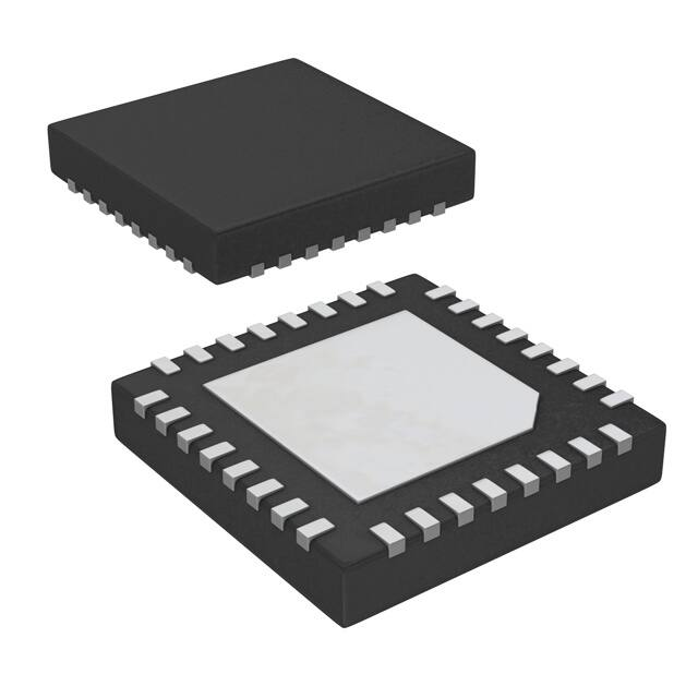
• 32 Ld 5x5 QFN Package - Near Chip-Scale Footprint
- Enhanced Thermal Performance for MHz Applications
Ordering Information
• Pb-Free (RoHS compliant)
PART
NUMBER
(Note)
Applications
PART
MARKING
TEMP.
RANGE
(°C)
PACKAGE PKG.
(Pb-free) DWG. #
• Power Supply for Datacom/Telecom and POL
ISL8120IRZEC
• Paralleling Power Module
ISL8120IRZ-TEC* ISL8120 IRZ -40 to +85 32 Ld QFN L32.5x5B
• Wide and Narrow Input Voltage Range Buck Regulators
*Please refer to TB347 for details on reel specifications.
NOTE: These Intersil Pb-free plastic packaged products employ
special Pb-free material sets, molding compounds/die attach
materials, and 100% matte tin plate plus anneal (e3 termination
finish, which is RoHS compliant and compatible with both SnPb and
Pb-free soldering operations). Intersil Pb-free products are MSL
classified at Pb-free peak reflow temperatures that meet or exceed
the Pb-free requirements of IPC/JEDEC J STD-020.
• DDR I and II Applications
• High Current Density Power Supplies
• Multiple Outputs VRM and VRD
Pinout
ISL8120 IRZ -40 to +85 32 Ld QFN L32.5x5B
FB1
VMON1
VSEN1-
VSEN1+
ISEN1B
ISEN1A
VCC
BOOT1
ISL8120IRZEC
(32 LD QFN)
TOP VIEW
32
31
30
29
28
27
26
25
COMP1 1
24 UGATE1
ISET 2
23 PHASE1
ISHARE 3
22 LGATE1
EN/VFF1 4
21 PVCC
33
GND
FSYNC 5
20 LGATE2
EN/VFF2 6
19 PHASE2
CLKOUT/REFIN 7
18 UGATE2
17 BOOT2
FN6763 Rev.2.00
November 11, 2011
9
10
11
12
13
14
15
16
COMP2
FB2
VMON2
VSEN2-
VSEN2+
ISEN2B
ISEN2A
VIN
PGOOD 8
Page 2 of 33
�EN/FF1
PVCC
VCC
ISL8120IR
FN6763 Rev.2.00
November 11, 2011
Block Diagram (1/2)
VIN
INTERNAL
LINEAR REGULATOR
POWER-ON
RESET (POR)
5.4V
OTP
OVER-TEMPERATURE
PROTECTION (OTP)
CHANNEL 1
REFERENCE
VREF = 0.6V
SOFT-START AND
FAULT LOGIC
VCC
UGATE1
VREF
700mV
BOOT1
SAW1
AVG_OCP
+
FB1
E/A1
7-CYCLE
DELAY
COMP1
PHASE1
GATE
CONTROL
PWM1
-
PVCC
OV/UV
COMP1
CHANNEL1
OCP
ICSH_ERR
CORRECTION
IAVG_CS
AVERAGE
OCP
1V
VSEN1+
CURRENT
ICS1
ISHARE
CHANNEL 1
UNITY GAIN
DIFF AMP1
PGOOD
COMP1
PGOOD
ISEN1A
CURRENT
SAMPLING
105µA
VSEN1-
LGATE1
CURRENT
CORRECTION
ISEN1B
ICSH_ERR
(BOTTOM PAD) GND
Page 3 of 33
VMON1
PGOOD
FIGURE 1. CHANNEL/PHASE 1 (VDDQ)
�ISHARE
CLKOUT/REFIN FSYNC
EN/FF2
ICSH_ERR
RELATIVE
PHASE
CONTROL
ISL8120IR
FN6763 Rev.2.00
November 11, 2011
Block Diagram (2/2)
IAVG_CS+15µA
CURRENT
SHARE
BLOCK
SAW1
IAVG_CS+15µA
ISET
IAVG_CS
OTP POR
k*VDDQ
VREF
CHANNEL 2
VCC
MASTER CLOCK
OSCILLATOR
GENERATOR
ICS1
+
ICS2
+
AVERAGE
IAVG
SOFT-START AND
FAULT LOGIC
BOOT2
PVCC
VREF2
700mV
UGATE2
SAW2
M/D CONTROL
AVG_OCP
FB2
E/A2
7-CYCLE
DELAY
COMP2
+
PWM2
OV/UV
COMP2
PHASE2
GATE
CONTROL
-
CURRENT
VREF
M/D
CONTROL
CURRENT
CORRECTION
PVCC
-
LGATE2
+
CHANNEL2
OCP
ICS2
GND
CHANNEL 2
105µA
VSEN2+
VSEN2-
PGOOD
COMP2
UNITY GAIN
DIFF AMP2
ISEN2A
CURRENT
SAMPLING
ISEN2B
PGOOD
M/D = 1: multiphase
VMON2
Page 4 of 33
M/D = 0: DUAL OUTPUT OPERATION
IAVG_CS = IAVG or ICS1
IAVG = (ICS1 + ICS2) / 2
ICSH_ERR = (VISARE - VISET)/GCS
0.6V =k*VDDQ
FIGURE 2. CHANNEL/PHASE 2 (VTT)
�ISL8120IR
Typical Application I (Dual Regulators with DCR Sensing and Remote Sense)
VIN
+3.3 TO +22V
VIN_F
RCC
CF2
LIN
CHFIN
CBIN
CF1
VCC
PVCC
BOOT1
CBOOT1
UGATE1
VIN
Q1
LOUT1
PHASE1
CF3
VOUT1
COUT1
LGATE1
Q2
2k
ISEN1A
COMP1
ISL8120IRZEC
10
RISEN1
ISEN1B
10
ZCOMP1
FB1
VCC
CLKOUT/REFIN
ZFB1
VMON1
VSENSE1+
RFB1
VSEN1+
ROS1
VSEN1-
PGOOD
CSEN1
VSENSE1-
VIN_F
BOOT2
CBOOT2
RFS
UGATE2
FSYNC
Q3
LOUT2
PHASE2
VOUT2
Q4
LGATE2
COUT2
2k
ISEN2A
10
ISEN2B
COMP2
EN2/FF2
RISEN2
10
ZCOMP2
FB2
EN1/FF1
ZFB2
RSET
VMON2
ISET
GND
FN6763 Rev.2.00
November 11, 2011
RFB2
VSEN2+
ISHARE
VSEN2-
ROS2
CSEN2
VSENSE2+
VSENSE2-
Page 5 of 33
�ISL8120IR
Typical Application II (Double Data Rate I or II)
VIN
+3.3 TO +22V
VIN_F
RCC
CF2
LIN
CHFIN
CBIN
CF1
VCC
PVCC
BOOT1
CBOOT1
UGATE1
VIN
2.5V
1.8V
LOUT1
PHASE1
CF3
RFS
Q1
(DDR I)
(DDR II)
VDDQ
COUT1
LGATE1
FSYNC
Q2
2k
ISEN1A
COMP1
ISL8120IRZEC
10
RISEN1
ISEN1B
10
ZCOMP1
FB1
ZFB1
VMON1
VSENSE1+
RFB1
VSEN1+
VDDQ
ROS1
VSEN1-
CSEN1
VSENSE1-
R*(VDDQ/0.6-1)
(See notes below)
CLKOUT/REFIN
1nF
R
VDDQ Or VIN_F
BOOT2
CBOOT2
UGATE2
(Or tie REFIN pin to VMON1 pin)
Q3
1.25V (DDR I)
0.9V (DDR II)
LOUT2
PHASE2
VTT
LGATE2
COUT2
Q4
( VDDQ/2)
2k
ISEN2A
10
ISEN2B
COMP2
RISEN2
10
ZCOMP1
FB2
PGOOD
ZFB1
VMON2
RSET
ISET
RFB2
VSEN2+
ISHARE
GND
VSEN2-
ROS2
CSEN2
VSENSE2+
VSENSE2-
Note 1: Set the upper resistor to be a little higher than R*(VDDQ/0.6 - 1) will set the final REFIN voltage (stead state voltage after soft-start) derived from
the VDDQ to be a little higher than internal 0.6V reference. In this way, the VTT final voltage will use the internal 0.6V reference after soft-start.
Note 2: Another way to set REFIN voltage is to connect VMON1 directly to REFIN pin.
FN6763 Rev.2.00
November 11, 2011
Page 6 of 33
�ISL8120IR
Typical Application III (2-Phase Operation with rDS(ON) Sensing and Voltage Trimming)
VIN
+3V TO +22V
LIN
CHFIN
CF1
RCC
VCC
CBIN
CF2
PVCC
BOOT1
CBOOT1
UGATE1
VIN
Q1
LOUT1
VOUT1
PHASE1
CF3
EN/FF1,2
COUT1
Q2
LGATE1
ISEN1A
10
RISEN1
ISEN1B
ISL8120IRZEC
COMP1/2
10
VSENSE1+
VSENSE1-
ZCOMP1
FB1
RSET
ISET
DNP
VMON1/2
ISHARE
RFB1
VSEN1+
ROS1
VSEN1-
0
CSEN1
PULLED TO VSENSE1TRIM UP
TRIM DOWN
PGOOD
PULLED TO VSENSE1+
VIN_F
BOOT2
CBOOT2
RFS
UGATE2
FSYNC
Q3
LOUT2
PHASE2
LGATE2
ISEN2A
CLKOUT/REFIN
RISEN2
ISEN2B
GND
Q4
VCC
FB2
VSEN2-
VSEN2+
GND
FN6763 Rev.2.00
November 11, 2011
Page 7 of 33
�ISL8120IR
Typical Application IV (3-Phase Regulator with Precision Resistor Sensing)
VIN
LIN
+3V TO +22V
RCC
VCC
CF1
VIN_F
CIN
CF2
PVCC
BOOT1
CBOOT2
VIN
CF3
UGATE1
LOUT2
VOUT
PHASE1
ISL8120IRZEC
EN/FF1
Q1
LGATE1
PHASE 2
COUT
Q2
ISEN1A
CLKOUT/REFIN
PGOOD
RISEN2
ISEN1B
COMP1
10
FB1
BOOT2
10
VMON1
UGATE2
PHASE2
VSEN1+
LGATE2
VSEN1-
ISEN2A
VSENSE1+
VCC
VSENSE1-
GND
ISEN2B
EN/FF2
GND
FSYNC
FB2
VMON2
ISHARE
VSEN2+
ISET
VSEN2-
RCC
VCC
CF1
VIN
FSYNC
EN/FF1,2
BOOT2
Q3
CBOOT1
LOUT1
LGATE1
Q2
ISL8120IRZEC
PHASE 1 AND 3
UGATE2
ISEN1A
RISEN1
ISEN1B
COMP1/2
PHASE2
Q4
Q1
PHASE1
EN/FF1,2
PGOOD
LOUT3
VIN_F
UGATE1
RFS
CBOOT3
CF2
PVCC
BOOT1
CF3
VIN_F
R
R
ZCOMP1
FB1
ZFB1
VMON1/2
LGATE2
RFB1
VSEN1+
ISEN2A
VSEN1-
ROS1
CSEN1
ISEN2B
RISEN3
VCC
GND
VCC
ISHARE
FB2
VSEN2+
R
VSEN2-
CLKOUT/REFIN
GND
ISET
R
FN6763 Rev.2.00
November 11, 2011
Page 8 of 33
�ISL8120IR
Typical Application V (4 Phase Operation with DCR Sensing)
VIN
LIN
+3V TO +22V
VIN_F
CIN
VCC
CF1
RCC
CF2
PVCC
BOOT1
CBOOT2
VIN
CF3
UGATE1
CLKOUT/REFIN
Q1
LGATE1
EN/FF1,2
VCC
VCC
VCC
VIN_F
FB2
ISL8120IRZEC
ISEN1A
PHASE 2 AND 4
ISEN1B
VSEN1,2BOOT2
Q3
Q4
10
RISEN2
COMP1/2
10
FB1
CBOOT4
LOUT4
UGATE2
VMON1/2
PHASE2
ISET
ISEN2A
RFB1
COS
ROS1
R
GND
LGATE2
VOUT1
COUT
Q2
PGOOD
VSEN1,2+
LOUT2
PHASE1
2ND DIVIDER TO AVOID
SINGLE POINT FAILURE
VSENSE1+
VSENSE1-
FSYNC
ISEN2B
ISHARE
RISEN4
R
VCC
CF1
RCC
CF2
PVCC
VIN_F
BOOT1
VIN
FSYNC
CF3
UGATE1
Q1
CBOOT1
LOUT1
PHASE1
RFS
LGATE1
EN/FF1,2
Q2
PGOOD
VIN_F
BOOT2
CBOOT3
LOUT3
Q3
ISL8120IRZEC
ISEN1A
PHASE 1 AND 3
ISEN1B
UGATE2
COMP1/2
PHASE2
RISEN1
ZCOMP1
ZFB1
FB1
VMON1/2
Q4
LGATE2
RFB1
VSEN1+
ISEN2A
RISEN3
VSEN1-
ROS1
CSEN1
ISEN2B
VCC
VCC
VCC
ISHARE
FB2
VSEN2+
R
VSEN2-
CLKOUT/REFIN
GND
ISET
R
FN6763 Rev.2.00
November 11, 2011
Page 9 of 33
�ISL8120IR
Typical Application VI (3-Phase Regulator with Resistor Sensing and 1 Phase Regulator)
VIN
LIN
+3V TO +22V
VCC
CF1
RCC
CBOOT2
VIN
UGATE1
LGATE1
EN/FF1
PGOOD
VCC
Q3
FB1
PHASE2
VMON1
ISL8120IRZEC
COUT1
Q2
RISEN2
VSEN1-
ISEN2A
10
VSENSE1+
VCC
ISET
10
ISEN2B
10
ZFB2
RISEN4
FSYNC
FB2
ISHARE
VMON2
VSEN2+
VSEN2-
VSENSE1R
ZCOMP2
VSENSE2+
10
VSEN1+
LGATE2
Q4
VOUT1
ISEN1B
COMP1
UGATE2
COUT2
PHASE 2
LOUT2
ISEN1A
CLKOUT/REFIN
BOOT2
LOUT4
VOUT2
Q1
PHASE1
EN/FF2
CBOOT4
CIN
CF2
PVCC
BOOT1
CF3
VIN_F
VIN_F
GND
R
PHASE 2
VSENSE2-
VCC
CF1
RCC
CF2 VIN_F
PVCC
BOOT1
VIN
FSYNC
CF3
UGATE1
CBOOT1
LOUT1
Q1
PHASE1
RFS
LGATE1
PGOOD
Q2
EN/FF1, 2
VIN_F
BOOT2
CBOOT3
LOUT3
Q3
ISL8120IRZEC
RISEN1
ISEN1B
UGATE2
COMP1/2
PHASE2
Q4
ISEN1A
ZCOMP1
FB1
ZFB1
VMON1/2
LGATE2
RFB1
VSEN1+
ISEN2A
VSEN1-
ROS1
CSEN1
ISEN2B
RISEN3
VCC
GND
VCC
ISHARE
FB2
VSEN2+
PHASE 1 AND 3
VSEN2-
R
ISET
VSEN2+
FN6763 Rev.2.00
November 11, 2011
CLKOUT/REFIN
GND
R
Page 10 of 33
�ISL8120IR
Typical Application VII (6 Phase Operation with DCR Sensing)
+3V TO +22V
VIN
VIN_F
LIN
RCC
VCC
CF1
VIN
CLKOUT/REFIN
CF3
EN/FF1, 2
PVCC
BOOT1
CIN
CF2
UGATE1
PHASE1
Q1
LGATE1
Q2
PGOOD
GND
VCC
VIN_F
CBOOT6
LOUT6
FB2
VSEN2+
VSEN2BOOT2
Q3
Q4
ISL8120IRZEC
PHASE 3 AND 6
UGATE2
PHASE2
LGATE2
ISEN1A
ISEN1B
COMP1/2
FB1
VMON1/2
VSEN1+
VSEN1ISET
RISEN3
VCC
R
ISEN2A
FSYNC
ISEN2B
ISHARE
GND
RISEN6
R
VCC
CF1
RCC
VIN
CF3
EN/FF1, 2
PVCC
BOOT1
VIN_F
CF2
UGATE1
PHASE1
Q1
LGATE1
Q2
PGOOD
VIN_F
CBOOT5
LOUT5
Q3
GND
VCC
UGATE2
PHASE2
ISL8120IRZEC
LGATE2
RISEN2
COMP1/2
FB1
VMON1/2
VSEN1+
VSEN1-
ISEN2A
VCC
CLKOUT/REFIN
ISEN2B
FSYNC
FB2
VSEN2+
VSEN2-
CBOOT2
LOUT2
ISEN1A
ISEN1B
BOOT2
Q4
RISEN5
CBOOT3
LOUT3
PHASE 2 AND 5
GND
ISHARE
ISET
R
R
VIN_F
VCC
CF1
CF3
FSYNC
RCC
VIN
EN/FF1, 2
PGOOD
VIN_F
CBOOT4
LOUT4
UGATE2
PHASE2
ISL8120IRZEC
Q4
LGATE2
RISEN4
GND
VCC
FB2
VSEN2+
VSEN2-
LGATE1
Q2
PHASE 1 AND 4
CBOOT1
LOUT1
VOUT1
COUT1
RISEN1
ZCOMP1
10
ZFB1
10
VMON2
ROS1
VSEN1ISHARE
GND
FN6763 Rev.2.00
November 11, 2011
Q1
VSEN1+
ISEN2A
ISEN2B
CF2
UGATE1
PHASE1
ISEN1A
ISEN1B
VMON1
FB1
COMP1/2
BOOT2
Q3
PVCC
BOOT1
CLKOUT/REFIN
ISET
RFB1
ROS1
RFB1
CSEN1
VSENSE1+
VSENSE1-
R
R
Page 11 of 33
�ISL8120IR
Typical Application VIII (Multiple Power Modules in Parallel with Current Sharing Control)
VIN
LIN
+3V TO +22V
VIN_F
CIN
VCC
CF4
RCC2
BOOT1
CBOOT3
VIN
CF6
CF5
PVCC
UGATE1
PGOOD
Q5
LOUT3
VOUT2
PHASE1
CLKOUT/REFIN
LGATE1
COUT2
Q6
EN/FF1, 2
ISEN1A
VIN_F
BOOT2
ISEN1B
CBOOT4
LOUT4
PHASE2
COMP1/2
ISL8120IRZEC
Q8
LGATE2
10
ZCOMP2
ZFB2
FB1
VMON1/2
RFB2
VSEN1+
ISEN2A
RISEN4
GND
VCC
2-PHASE
MODULE #1
ROS2
RCSR2
VSEN1-
ISEN2B
VSEN2+
FB2
10
RISEN3
UGATE2
Q7
CSEN2
VSENSE2+
VSENSE2VLOAD
FSYNC
ISHARE
VSEN2-
GND
ISET
R
R
VCC
CF1
RCC1
VIN_F
CF2
PVCC
BOOT1
VIN
FSYNC
CF3
UGATE1
Q1
CBOOT1
LOUT1
VOUT1
PHASE1
RFS
LGATE1
EN/FF1, 2
COUT1
Q2
PGOOD
VIN_F
ISEN1A
BOOT2
LOUT2
Q3
UGATE2
COMP1/2
PHASE2
10
ZCOMP1
ZFB1
FB1
ISL8120IRZEC
Q4
RISEN1
ISEN1B
CBOOT2
LGATE2
RFB1
VSEN1+
ISEN2A
RISEN2
10
VMON1/2
VSEN1-
RCSR1
ROS1
CSEN1
VSENSE1+
VSENSE1-
ISEN2B
VSEN2+
GND
VCC
FB2
2-PHASE
ISHARE
R
MODULE #2
CLKOUT/REFIN
VSEN2GND
ISET
R
FN6763 Rev.2.00
November 11, 2011
Page 12 of 33
�ISL8120IR
Typical Application VIIII (4 Outputs Operation with DCR Sensing)
VIN
LIN
+3V TO +22V
CF3
VSENSE4+
EN/FF2
VSEN2+
RFB4
VSENSE4ZFB3
2
PVCC
BOOT1
VIN
CLKOUT/REFIN
CSEN4
ROS4
2
RCC
VCC
CF1
VIN_F
COUT4 CBOOT6
LOUT6
VOUT4
VSEN2VMON2
FB2
ZCOMP4 COMP2
PGOOD
BOOT2
Q4
Q1
LGATE1
Q2
CBOOT3
LOUT3
VOUT3
COUT3
(PHASE 3 AND 6)
2
RISEN3
2
ZFB3
RFB3
VSEN1+
ROS3
VSEN1ISHARE/ISET
EN/FF1
R
FSYNC
VSENSE3+
CSEN3
VSENSE3-
ISEN2A OUTPUT 3 AND 4 GND
ISEN2B
RCC
VCC
CF1
PVCC
BOOT1
VIN
CF3
EN/FF1, 2
PGOOD
VIN_F
LOUT5
UGATE1
PHASE1
COMP1
FB1
VMON1
ISL8120IRZEC
LGATE2
RISEN6
CBOOT2
CF2
ISEN1A
ISEN1B
UGATE2
PHASE2
Q3
VIN_F
CIN
BOOT2
Q4
LGATE2
ISL8120IRZEC
(PHASE 2 AND 5)
VCC
LGATE1
Q2
CBOOT1
LOUT2
VOUT2
COUT2
RISEN2
2
2
RFB2
CSEN2
ROS2
VSEN1CLKOUT/REFIN
FSYNC
ISEN2B
GND
Q1
COMP1/2 ZCOMP2
FB1
ZFB2
VMON1/2
VSEN1+
ISEN2A
RISEN5
UGATE1
PHASE1
ISEN1A
ISEN1B
UGATE2
PHASE2
Q3
VIN_F
CF2
VSENSE2+
VSENSE2-
ISHARE/ISET
FB2
VSEN2+
VSEN2-
OUTPUT 2
GND
R
VIN_F
VCC
CF1
FSYNC
CF3
RCC
VIN
EN/FF1, 2
PGOOD
VIN_F
CBOOT4
LOUT4
BOOT2
Q3
Q4
UGATE2
PHASE2
LGATE2
ISL8120IRZEC
(PHASE 1 AND 4)
GND
VCC
FB2
VSEN2+
VSEN2-
CF2
UGATE1
PHASE1
Q1
LGATE1
Q2
ISEN1A
ISEN1B
VMON1
FB1
COMP1/2
VOUT1
COUT1
RISEN1
ZCOMP1
ROS1
2
ZFB1
RFB1
ROS1
VSEN1ISHARE/ISET
OUTPUT 1
CBOOT1
LOUT1
2
VMON2
VSEN1+
ISEN2A
ISEN2B
RISEN4
PVCC
BOOT1
CLKOUT/REFIN
RFB1
CSEN1
VSENSE1+
VSENSE1-
R
GND
FN6763 Rev.2.00
November 11, 2011
Page 13 of 33
�ISL8120IR
Absolute Maximum Ratings
Thermal Information
Input Voltage, VIN . . . . . . . . . . . . . . . . . . . . . . . . . . . . -0.3V to +27V
Driver Bias Voltage, PVCC . . . . . . . . . . . . . . . . . . . . -0.3V to +6.5V
Signal Bias Voltage, VCC . . . . . . . . . . . . . . . . . . . . . -0.3V to +6.5V
BOOT/UGATE Voltage, VBOOT . . . . . . . . . . . . . . . . . . -0.3V to +36V
Phase Voltage, VPHASE . . . . . . . . . . VBOOT - 7V to VBOOT + 0.3V
BOOT to PHASE Voltage, VBOOT - VPHASE . . -0.3V to VCC +0.3V
Input, Output or I/O Voltage . . . . . . . . . . . . . . . . -0.3V to VCC +0.3V
Thermal Resistance (Typical Notes 1, 2)
JA(°C/W)
JC(°C/W)
32 Ld QFN Package . . . . . . . . . . . . . . 32
3.5
Maximum Junction Temperature . . . . . . . . . . . . . . .-55°C to +150°C
Maximum Storage Temperature Range . . . . . . . . . .-65°C to +150°C
Pb-free Reflow Profile . . . . . . . . . . . . . . . . . . . . . . . . .see link below
http://www.intersil.com/pbfree/Pb-FreeReflow.asp
Recommended Operating Conditions
Input Voltage, VIN . . . . . . . . . . . . . . . . . . . . . . . . . . . . . . . 3V to 22V
Driver Bias Voltage, PVCC . . . . . . . . . . . . . . . . . . . . . . . 3V to 5.6V
Signal Bias Voltage, VCC . . . . . . . . . . . . . . . . . . . . . . . . 3V to 5.6V
Boot to Phase Voltage (Overcharged), VBOOT - VPHASE . . . . . .


 工商网监
湘ICP备2023018690号
工商网监
湘ICP备2023018690号

