DATASHEET
ISL8560
FN9244
Rev 7.00
September 19, 2008
DC/DC Power Switching Regulator
The ISL8560 is a step down DC/DC power switching
regulator which accepts 9.0V to 60V input and provides a 2A
output current. The output voltage can be set in the range
between 1.21V and 55V by means of an external divider.
The device uses an internal power DMOS transistor with a
typical rDS(ON) of 0.19 to obtain very high efficiency and
high switching speed. A switching frequency in the range of
100kHz to 600kHz can be realized (the maximum power
dissipation of the various packages must be observed).
Notable features of this next generation of DC/DC converter
includes pulse-by-pulse current limit for FET protection,
hiccup mode for short circuit protection, voltage feedforward
regulation, Frequency SYNC, soft-start, low standby current
of 60µA typical in the disabled state, and thermal shut-down.
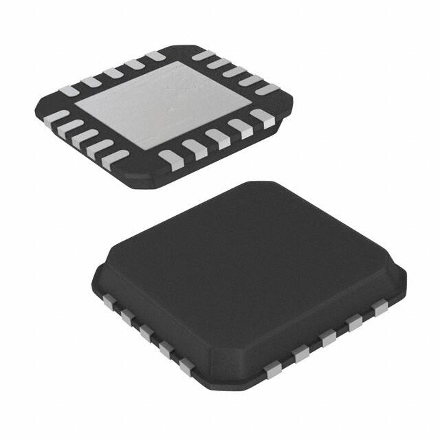
The device is available in a 20 Ld QFN package.
Features
• Voltage feedforward mode
• Step down DC/DC supporting up to 2A
• Input voltage range of 9.0V to 60V
• Internal reference of 1.21V ±1%
• Adjustable output voltage range of 1.21V to 55V
• Adjustable switching frequency 100kHz to 600kHz
• Frequency SYNC pin
• Zero load current operation
• Pulse-by-pulse mode current limit and Hiccup mode
• Low standby current of 60µA typical
• Thermal shut-down
Ordering Information
PART
NUMBER
(Note)
ISL8560IRZ
PART
MARKING
TEMP.
RANGE
(°C)
• Load dump to 100V for 400ms
PACKAGE
(Pb-Free)
PKG.
DWG. #
ISL 8560IRZ -40 to +85 20 Ld 6x6 QFN L20.6x6B
ISL8560IRZ-T* ISL 8560IRZ -40 to +85 20 Ld 6x6 QFN L20.6x6B
*Please refer to TB347 for details on reel specifications.
NOTE: These Intersil Pb-free plastic packaged products employ
special Pb-free material sets, molding compounds/die attach
materials, and 100% matte tin plate plus anneal (e3 termination
finish, which is RoHS compliant and compatible with both SnPb and
Pb-free soldering operations). Intersil Pb-free products are MSL
classified at Pb-free peak reflow temperatures that meet or exceed
the Pb-free requirements of IPC/JEDEC J STD-020.
• Pb-Free (RoHS compliant)
Applications
• Industrial and automotive power supplies
• Portable computers
• Battery chargers
• Distributed power systems
Related Literature
• Technical Brief TB363 “Guidelines for Handling and
Processing Moisture Sensitive Surface Mount Devices
(SMDs)”
Pinout
FN9244 Rev 7.00
September 19, 2008
VIN
VIN
VIN
VIN
LX
ISL8560
(20 LD QFN)
TOP VIEW
20
19
18
17
16
2
14
SS
BOOT
3
13
PGND
EN
4
12
PGOOD
VCC5
5
11
REF
6
7
8
9
10
COMP
LX
FB
LX
SGND
15
RTCT
1
SYNC
LX
Page 1 of 17
�ISL8560
Absolute Maximum Ratings
Thermal Information
Input Voltage VIN . . . . . . . . . . . . . . . . . . . . . . . . . GND - 0.3V to 72V
Voltage at BOOT pin . . . . . . . . . . . . . . . . . . . . . . GND - 0.3V to 82V
LX, RTCT . . . . . . . . . . . . . . . . . . . . . . . . . . . . . . . GND - 0.3V to 60V
REF, FB, SS, EN, SYNC, PGOOD pins. . . . . . . . . . . . . . . . . . . . .8V
VCC5* . . . . . . . . . . . . . . . . . . . . . . . . . . . . . . . . GND - 0.3V to 5.5V
Thermal Resistance (Typical, Notes 1, 2) JA (°C/W) JC (°C/W)
QFN Package. . . . . . . . . . . . . . . . . . . .
30
1.5
Maximum Power Dissipation. . . . . . . . . . . . . . . . . . . . . . . . . . . . . . . . 3W
Maximum Junction Temperature (Hermetic Package or Die) . . +150°C
Maximum Junction Temperature (Plastic Package) . . . . . . . +150°C
Maximum Storage Temperature Range . . . . . . . . . .-65°C to +150°C
Pb-Free Reflow Profile. . . . . . . . . . . . . . . . . . . . . . . . .see link below
http://www.intersil.com/pbfree/Pb-FreeReflow.asp
Recommended Operating Conditions
Junction Temperature Range. . . . . . . . . . . . . . . . . .-40°C to +125°C
Supply Voltage Range (Typical). . . . . . . . . . . . . . . . . . . 9.0V to 60V
CAUTION: Do not operate at or near the maximum ratings listed for extended periods of time. Exposure to such conditions may adversely impact product reliability and
result in failures not covered by warranty.
*An accidental short between VCC5 and GND may cause excessive heating and permanent damage to the device.
NOTES:
1. JA is measured in free air with the component mounted on a high effective thermal conductivity test board with “direct attach” features. See
Tech Brief TB379.
2. For JC, the “case temp” location is the center of the exposed metal pad on the package underside.
3. Additional heatsinking may be required to insure that the junction temperature does not exceed above +125°C.
Electrical Specifications
PARAMETER
Unless otherwise specified the specifications listed in the table are tested at TA = +25°C and guard band for the
full Temperature Range, VIN = 48V, VOUT = 5.0V, IOUT = 0A. Typical values are at TA = +25°C. Parameters
with MIN and/or MAX limits are 100% tested at +25°C, unless otherwise specified. Temperature limits
established by characterization and are not production tested.
SYMBOL
TEST CONDITIONS
MIN
TYP
MAX
UNITS
9.0
24
60
V
VIN = 9V, EN = HIGH
35
60
µA
VIN = 60V, EN = HIGH
60
110
µA
VIN = 9V, VFB = 1.5V
3.6
4
mA
VIN = 60V, VFB = 1.5V
6.0
8.0
mA
5.0
5.1
V
5
mA
8.9
V
0.55
V
VIN - 5
V
VIN SUPPLY
Input Voltage Range
VIN SUPPLY CURRENT
Shut-down Current
Operating Current
IDD
IDD
VCC5 SUPPLY (A 1µF capacitor is needed from VCC5 to GND)
VCC5 Output Voltage
VIN = 9.0V to 60V, IL = 0mA to 5mA
Maximum Output Current
VIN = 24V
4.9
INPUT UV
Rising UV Threshold
7.8
UV Threshold Hysteresis
0.18
0.3
BUCK CONVERTER
Output Voltage (Note 3)
IOUT = 2A
1.2
Maximum Duty Cycle
F = 300kHz
90
Minimum Controllable ON Time
96
%
F = 300kHz
150
ns
Over the VIN range with frequency set by
external resistor and capacitor at RTCT
±10
%
OSCILLATOR
Total Variation on Set Frequency
Frequency Range (Set by RTCT)
fOSC
100
600
kHz
SYNC Range
fOSC
100
600
kHz
Tested Oscillation Frequency
fOSC
FN9244 Rev 7.00
September 19, 2008
VIN = 9V to 60V, RT = 100k, CT = 1200pF
60
kHz
VIN = 9V to 60V, RT = 27.4k, CT = 220pF
725
kHz
Page 2 of 17
�ISL8560
Electrical Specifications
PARAMETER
Max Ramp Amplitude
Modulator Gain
Unless otherwise specified the specifications listed in the table are tested at TA = +25°C and guard band for the
full Temperature Range, VIN = 48V, VOUT = 5.0V, IOUT = 0A. Typical values are at TA = +25°C. Parameters
with MIN and/or MAX limits are 100% tested at +25°C, unless otherwise specified. Temperature limits
established by characterization and are not production tested. (Continued)
SYMBOL
VOSC
TEST CONDITIONS
MIN
VIN = 9V
VVIN/VOSC
Min OFF Time
TYP
MAX
UNITS
1
VP
9
-
150
300
ns
REFERENCE AND SOFT-START
Internal Reference Voltage
Soft-Start Current
Soft-Start Threshold
1.21
VREF
ISS
8
VSOFT
0.8
gm
3.9
10
V
12
µA
V
ERROR AMPLIFIER
Transconductance
Gain-Bandwidth Product
Slew Rate
COMP Pin Drive
5.7
7.2
mS
GBW
15
MHz
SR
6
V/µs
ICOMP
±200
µA
Internal Feedback Voltage
VFB
TA = -40°C to +85°C, VIN = 9.0V to 60V
Internal Feedback Bias Current
IFB
TA = -40°C to +85°C, VFB = 1.20V
1.194
1.210
1.222
V
±50
±100
nA
OVERCURRENT PROTECTION
Dynamic Current Limit ON Time
tOCON
16
Clock
pulses
Dynamic Current Limit OFF Time
tOCOFF
4
SS cycle
Switch Current Limit
ILIMIT
TA = +25°C
3.2
VPG-
Fraction of the VOUT set point; ~3µs noise filter
VPG+
Fraction of the VOUT set point; ~3µs noise filter
4.0
4.8
A
85
89
%
111
115
%
VPULLUP = 5.5V
1
µA
IPGOOD = 4mA
0.5
V
0.355
POWER-GOOD (OPEN DRAIN)
Power-Good Lower Threshold
PGOOD Leakage Current
IPGLKG
PGOOD Voltage Low
MOSFET
Switch ON-Resistance
rDS(ON)
IOUT = 2A, VBOOT = VIN + 5.0V, Tested at wafer
level
0.19
EN
Input HIGH Level (Asserted)
VINHIGH
Input LOW Level (Unasserted)
VINLOW
Input Current HIGH
IENHIGH
Input Current LOW
IENLOW
2.6
V
1.2
V
VIN = 24V
25
µA
VIN = 24V
25
µA
SYNC
Input HIGH Level (Asserted)
VINHIGH
2.6
V
Input LOW Level (Unasserted)
VINLOW
1.2
V
Input Current HIGH
ISYNCHIGH
0.2
µA
Input Current LOW
ISYNCLOW
0.2
µA
THERMAL SHUT-DOWN
Thermal Shut-down Temperature
Thermal Shut-down Hysteresis
FN9244 Rev 7.00
September 19, 2008
Rising Threshold
150
°C
15
°C
Page 3 of 17
�ISL8560
Pin Descriptions
SGND (Pin 8)
LX (Pins 1, 2, 15, 16)
The SGND terminal of the ISL8560 provides the return path
for the control and monitor portions of the IC.
There are four output pins that must be connected together
externally in normal operation.
BOOT (Pin 3)
A capacitor is connected from this pin to the output pin. An
internal 10V supply and an internal Schottky diode provide
the high side voltage to drive the gate of the output DMOS
device.
EN (Pin 4)
The EN input will disable the part and shut-down all function
when it is held high or left OPEN. The EN current will be
10µA typical. An internal pull-up resistor will hold the pin
high. When EN = Low, the part is enabled. Connect to GND
for auto start-up.
VCC5 (Pin 5)
VCC5 is the +5.0V output pin which provides an output of an
internal supply for supply filtering purposes. A 1µF capacitor
should be connected from this pin to GND. Internal VDD
supply is set at 5.0V (not planned that the user would use
this supply).
FB (Pin 9)
This is the feedback pin. The feedback ratio is set by an
external resistor divider connected to the load.
COMP (Pin 10)
This pin is connected to the output of the Error Amplifier and
is used to compensate the loop. The Error Amplifier is a GM
amplifier.
REF (Pin 11)
1.20V reference output. Bypass to GND with 0.01µF
capacitor.
PGOOD (Pin 12)
This pin is an open drain output that is turned on when the
feedback voltage is more than ±10% from the reference
voltage, indicating that the output is not within 10% of set
point.
PGND (Pin 13)
This pin is used as the ground connection of the power train.
SYNC (Pin 6)
SS (Pin 14)
This pin provides a digital input pin to synchronize the
internal oscillator to an external signal. When the sync
function is not used, this pin can be left open or tied to GND.
If the sync function is used, the RTCT timing must be set to a
frequency lower than the sync input frequency. The
termination of the ramp is synchronized with the rising edge
of the sync input signal. There are no duty cycle restrictions
on the input sync signal. Input thresholds are TTL
compatible.
A capacitor is connected from this pin to GND to determine
the soft-start timing. The soft-start pin internal charging
current is 10µA.
VIN (Pins 17, 18, 19, 20)
The input supply for the PWM regulator power stage.
Connected to DRAIN of the high side MOSFET.
RTCT (Pin 7)
A resistor to VIN and a capacitor to GND determine the
frequency of the saw-tooth oscillator. Resistor range is
R = 20k to 100k. Capacitor range is C = 470pF to 1.2nF. The
oscillator amplitude will vary from approximately 0.9V to 10V
as VIN changes from 8.5V to 60V to maintain constant
frequency and provide feed forward. The oscillator will have
a fixed off time, which will establish the maximum on time for
the regulator. This off time will be