DATASHEET
ISL88011, ISL88012, ISL88013, ISL88014, ISL88015
Data Sheet
December 4, 2015
5 Ld Voltage Supervisors with Adjustable Power-On Reset, Dual Voltage
Monitoring or Watchdog Timer Capability
The ISL88011, ISL88012, ISL88013, ISL88014, ISL88015
family of devices offer both fixed and/or adjustable
voltage-monitoring that combine popular functions such as
Power-On reset control, watchdog timer, supply voltage
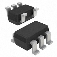
supervision, and manual reset assertion in a small 5 Ld
SOT-23 package.
Unique features on the ISL88013 and ISL88015 include a
watchdog timer with a 51s start-up timeout and a 1.6s
normal timeout duration. On the ISL88011 and ISL88014,
users can increase the nominal 200ms Power-On reset
timeout delay by adding an external capacitor to the CPOR
pin. Both fixed and adjustable voltage monitors are provided
by the ISL88012. Complementary active-low and active-high
reset outputs are available on the ISL88011, ISL88012 and
ISL88013 devices. All devices provide manual reset
capability (see “Product Features Table” on page 5).
Seven preprogrammed reset threshold voltages accurate to
±1.5% over temperature are offered (see “Ordering
Information” on page 3). The ISL88012, ISL88014 and
ISL88015 have a user-adjustable voltage input available for
custom monitoring of any voltage down to 0.6V. All parts are
specifically designed for low power consumption and high
threshold accuracy.
FN8093
Rev 5.00
December 4, 2015
Features
• Single/dual voltage monitoring supervisors
• Fixed-voltage options allow precise monitoring of +2.5V,
+3.0V, +3.3V, and +5.0V power supplies
• Dual supervisor has one fixed voltage input and another
that is user-adjustable down to 0.6V.
• Both RST and RST outputs available
• Adjustable POR timeout delay options
• Watchdog timer with 1.6s normal and 51s start-up timeout
durations
• Manual reset input on all devices
• Reset signal valid down to VDD = 1V
• Accurate ±1.5% voltage threshold
• Immune to power-supply transients
• Ultra low 5.5µA supply current
• Small 5 Ld SOT-23 Pb-Free package
• Pb-Free (RoHS Compliant)
Applications
• Process control systems
• Intelligent instruments
• Embedded control systems
• Computer systems
• Critical µP and µC power monitoring
• Portable/battery-powered equipment
• PDA and handheld PC devices
FN8093 Rev 5.00
December 4, 2015
Page 1 of 15
�ISL88011, ISL88012, ISL88013, ISL88014, ISL88015
Pinouts
ISL88012
(5 LD SOT-23)
TOP VIEW
ISL88011
(5 LD SOT-23)
TOP VIEW
RST/MR
1
GND
2
RST
3
5
4
VDD
CPOR
RST/MR
1
GND
2
RST
3
1
GND
2
RST
3
VDD
4
VMON
ISL88014
(5 LD SOT-23)
TOP VIEW
ISL88013
(5 LD SOT-23)
TOP VIEW
RST/MR
5
5
4
VDD
WDI
RST/MR
1
GND
2
VMON
3
5
VDD
4
CPOR
ISL88015
(5 LD SOT-23)
TOP VIEW
FN8093 Rev 5.00
December 4, 2015
RST/MR
1
GND
2
VMON
3
5
VDD
4
WDI
Page 2 of 15
�ISL88011, ISL88012, ISL88013, ISL88014, ISL88015
Ordering Information
PART NUMBER
(Notes 1, 2, 3)
PART
MARKING VTHVDD VTHVMON
(Note 4)
(V)
(V)
TEMPERATURE
RANGE
(°C)
PACKAGE
TAPE AND REEL PKG.
(Pb-free)
DWG. #
ISL88011IH546Z-TK
AGU
4.64
N/A
-40 to +85
5 Ld SOT-23
P5.064
ISL88011IH546Z-T7A
AGU
4.64
N/A
-40 to +85
5 Ld SOT-23
P5.064
ISL88011IH544Z-TK
AGV
4.38
N/A
-40 to +85
5 Ld SOT-23
P5.064
ISL88011IH544Z-T7A
AGV
4.38
N/A
-40 to +85
5 Ld SOT-23
P5.064
ISL88011IH531Z-TK
AGW
3.09
N/A
-40 to +85
5 Ld SOT-23
P5.064
ISL88011IH531Z-T7A
AGW
3.09
N/A
-40 to +85
5 Ld SOT-23
P5.064
ISL88011IH529Z-TK
AGX
2.92
N/A
-40 to +85
5 Ld SOT-23
P5.064
ISL88011IH529Z-T7A
AGX
2.92
N/A
-40 to +85
5 Ld SOT-23
P5.064
ISL88011IH526Z-TK
AGY
2.63
N/A
-40 to +85
5 Ld SOT-23
P5.064
ISL88011IH526Z-T7A
AGY
2.63
N/A
-40 to +85
5 Ld SOT-23
P5.064
ISL88011IH523Z-TK
AGZ
2.32
N/A
-40 to +85
5 Ld SOT-23)
P5.064
ISL88011IH523Z-T7A
AGZ
2.32
N/A
-40 to +85
5 Ld SOT-23)
P5.064
ISL88011IH522Z-TK (No longer available, recommended AHE
replacement: ISL88013IH522Z-TK)
2.19
N/A
-40 to +85
5 Ld SOT-23
P5.064
AHE
2.19
N/A
-40 to +85
5 Ld SOT-23
P5.064
ISL88012IH546Z-TK (No longer available or supported) AHF
4.64
0.6 (Note 2)
-40 to +85
5 Ld SOT-23
P5.064
ISL88012IH546Z-T7A (No longer available or supported) AHF
4.64
0.6 (Note 2)
-40 to +85
5 Ld SOT-23
P5.064
ISL88012IH544Z-TK (No longer available or supported) AHG
4.38
0.6 (Note 2)
-40 to +85
5 Ld SOT-23
P5.064
ISL88012IH544Z-T7A (No longer available or supported) AHG
4.38
0.6 (Note 2)
-40 to +85
5 Ld SOT-23
P5.064
ISL88012IH531Z-TK (No longer available or supported) AHH
3.09
0.6 (Note 2)
-40 to +85
5 Ld SOT-23
P5.064
ISL88012IH531Z-T7A (No longer available or supported) AHH
3.09
0.6 (Note 2)
-40 to +85
5 Ld SOT-23
P5.064
ISL88012IH529Z-TK (No longer available or supported) AHI
2.92
0.6 (Note 2)
-40 to +85
5 Ld SOT-23
P5.064
ISL88012IH529Z-T7A (No longer available or supported) AHI
2.92
0.6 (Note 2)
-40 to +85
5 Ld SOT-23
P5.064
ISL88012IH526Z-TK (No longer available or supported) AHJ
2.63
0.6 (Note 2)
-40 to +85
5 Ld SOT-23
P5.064
ISL88012IH526Z-T7A (No longer available or supported) AHJ
2.63
0.6 (Note 2)
-40 to +85
5 Ld SOT-23
P5.064
ISL88012IH523Z-TK (No longer available or supported) AHK
2.32
0.6 (Note 2)
-40 to +85
5 Ld SOT-23
P5.064
ISL88012IH523Z-T7A (No longer available or supported) AHK
2.32
0.6 (Note 2)
-40 to +85
5 Ld SOT-23
P5.064
ISL88012IH522Z-TK (No longer available or supported) AHL
2.19
0.6 (Note 2)
-40 to +85
5 Ld SOT-23
P5.064
ISL88012IH522Z-T7A (No longer available or supported) AHL
2.19
0.6 (Note 2)
-40 to +85
5 Ld SOT-23
P5.064
ISL88013IH546Z-TK (No longer available, recommended AHM
replacement: ISL88011IH546Z-TK)
4.64
N/A
-40 to +85
5 Ld SOT-23
P5.064
ISL88013IH546Z-T7A (No longer available,
recommended replacement: ISL88011IH546Z-T7A)
AHM
4.64
N/A
-40 to +85
5 Ld SOT-23
P5.064
ISL88013IH544Z-TK
AHN
4.38
N/A
-40 to +85
5 Ld SOT-23
P5.064
ISL88013IH544Z-T7A
AHN
4.38
N/A
-40 to +85
5 Ld SOT-23
P5.064
ISL88013IH531Z-TK
AHO
3.09
N/A
-40 to +85
5 Ld SOT-23
P5.064
ISL88013IH531Z-T7A
AHO
3.09
N/A
-40 to +85
5 Ld SOT-23
P5.064
ISL88013IH529Z-TK
AHP
2.92
N/A
-40 to +85
5 Ld SOT-23
P5.064
ISL88013IH529Z-T7A
AHP
2.92
N/A
-40 to +85
5 Ld SOT-23
P5.064
ISL88011IH522Z-T7A (No longer available,
recommended replacement: ISL88013IH522Z-T7A)
FN8093 Rev 5.00
December 4, 2015
Page 3 of 15
�ISL88011, ISL88012, ISL88013, ISL88014, ISL88015
Ordering Information
(Continued)
PART
MARKING VTHVDD VTHVMON
(Note 4)
(V)
(V)
PART NUMBER
(Notes 1, 2, 3)
TEMPERATURE
RANGE
(°C)
PACKAGE
TAPE AND REEL PKG.
(Pb-free)
DWG. #
ISL88013IH526Z-TK
AHQ
2.63
N/A
-40 to +85
5 Ld SOT-23
P5.064
ISL88013IH526Z-T7A
AHQ
2.63
N/A
-40 to +85
5 Ld SOT-23
P5.064
ISL88013IH523Z-TK (No longer available,
recommended replacement: ISL88011IH523Z-TK)
AHR
2.32
N/A
-40 to +85
5 Ld SOT-23
P5.064
ISL88013IH523Z-T7A (No longer available,
recommended replacement: ISL88011IH523Z-T7A)
AHR
2.32
N/A
-40 to +85
5 Ld SOT-23
P5.064
ISL88013IH522Z-TK
AHS
2.19
N/A
-40 to +85
5 Ld SOT-23
P5.064
ISL88013IH522Z-T7A
AHS
2.19
N/A
-40 to +85
5 Ld SOT-23
P5.064
ISL88014IH5Z-TK
AHT
N/A
0.6 (Note 2)
-40 to +85
5 Ld SOT-23
P5.064
ISL88014IH5Z-T7A
AHT
N/A
0.6 (Note 2)
-40 to +85
5 Ld SOT-23
P5.064
ISL88015IH5Z-TK (No longer available or supported)
AHU
N/A
0.6 (Note 2)
-40 to +85
5 Ld SOT-23
P5.064
ISL88015IH5Z-T7A (No longer available or supported) AHU
N/A
0.6 (Note 2)
-40 to +85
5 Ld SOT-23
P5.064
ISL88011EVAL1Z
ISL88011 Evaluation Card
ISL88013EVAL1Z
ISL88013 Evaluation Card
ISL88014EVAL1Z
ISL88014 Evaluation Card
NOTES:
1. These Intersil Pb-free plastic packaged products employ special Pb-free material sets, molding compounds/die attach materials, and 100% matte
tin plate plus anneal (e3 termination finish, which is RoHS compliant and compatible with both SnPb and Pb-free soldering operations). Intersil Pbfree products are MSL classified at Pb-free peak reflow temperatures that meet or exceed the Pb-free requirements of IPC/JEDEC J STD-020.
2. The voltage trip point can be adjusted to be greater than 0.6V using 2 external resistors. By default, the VTHVMON trip point is 0.6V if no external
resistors are used.
3. For Moisture Sensitivity Level (MSL), please see device information page for ISL88011, ISL88012, ISL88013, ISL88014, ISL88015. For more
information on MSL please see techbrief TB363.
4. The part marking is located on the bottom of the part.
Functional Block Diagrams
VDD
VDD
VDD
RST/MR
RST/MR
POR
± VTHMON
RST/MR
POR
PB
VDD
POR
PB
± VTHMON
OSC
VMON
CPOR
PB
± VTHMON
RST
RST
RST
OSC
WDI
± VREF
GND
GND
ISL88011
GND
ISL88012
ISL88013
VDD
VDD
R1
R1
RST/MR
VMON
R2
WDT
POR
± VTHMON
PB
VDD
RST/MR
VMON
R2
POR
PB
± VTHMON
OSC
CPOR
OSC
GND
ISL88014
FN8093 Rev 5.00
December 4, 2015
WDI
WDT
GND
ISL88015
Page 4 of 15
�ISL88011, ISL88012, ISL88013, ISL88014, ISL88015
Product Features Table
FUNCTION
ISL88011
ISL88012
ISL88013
ISL88014
ISL88015
Active-Low Reset (RST)
x
x
x
x
x
Active-High Reset (RST)
x
x
x
Watchdog Timer (WDI)
x
Dual Voltage Supervision
x
x
Adjustable POR Timeout (CPOR)
x
Manual Reset Input (MR)
x
x
x
Fixed Trip Point Voltage
x
x
x
Adjustable Trip Point Voltage
x
x
x
x
x
x
Pin Descriptions
PIN
ISL88011
ISL88012
ISL88013
ISL88014
ISL88015
NAME
1
1
1
1
1
RST/MR
2
2
2
2
2
GND
3
3
VMON
4
3
3
3
4
RST
4
4
5
5
FN8093 Rev 5.00
December 4, 2015
5
5
CPOR
FUNCTION
Combined Active-Low Reset Output and Manual Reset Input
Ground
Adjustable Threshold Voltage Input
Active-High Reset Output
Adjustable POR Timeout Delay Input
4
WDI
Watchdog Timer Input
5
VDD
Supply Voltage and Monitored Input
Page 5 of 15
�ISL88011, ISL88012, ISL88013, ISL88014, ISL88015
R
Absolute Maximum Ratings
Thermal Information
Temperature Under Bias . . . . . . . . . . . . . . . . . . . . .-40°C to +125°C
Storage Temperature . . . . . . . . . . . . . . . . . . . . . . .-65°C to +150°C
Voltage on any pin with respect to GND . . . . . . . . . . . . -1.0V to +7V
DC Output Current . . . . . . . . . . . . . . . . . . . . . . . . . . . . . . . . . . . 5mA
ESD Rating
Human Body Model (Tested per JESD22-A114) . . . . . . . . .2500V
Charged Device Model (Tested per JESD22-C101E) . . . . .1200V
Machine Model (Tested per JESD22-A115) . . . . . . . . . . . . .250V
Thermal Resistance (Typical
JA (°C/W)
5 Ld SOT-23 (Note 5). . . . . . . . . . . . . . . . . . . . . . . .
190
Maximum Junction Temperature (Plastic Package) . . . . . . . +125°C
Maximum Storage Temperature Range . . . . . . . . . .-65°C to +150°C
Pb-Free Reflow Profile. . . . . . . . . . . . . . . . . . . . . . . . .see link below
http://www.intersil.com/pbfree/Pb-FreeReflow.asp
Recommended Operating Conditions
Temperature Range (Industrial) . . . . . . . . . . . . . . . . .-40°C to +85°C
Pull-up Resistance (RPU) . . . . . . . . . . . . . . . . . . . . . 5k to 100k
CAUTION: Do not operate at or near the maximum ratings listed for extended periods of time. Exposure to such conditions may adversely impact
product reliability and result in failures not covered by warranty.
NOTE:
5. JA is measured with the component mounted on a high effective thermal conductivity test board in free air. See Tech Brief TB379 for details.
Electrical Specifications
SYMBOL
Over the recommended operating conditions unless otherwise specified, RPU = 10k.
PARAMETER
TEST CONDITIONS
MAX
UNITS
5.5
V
8
11.5
µA
7
10
µA
VDD = 2.5V
5.5
9
µA
VDD = 3.3V
4.5
8
µA
VDD
Supply Voltage Range
IDD
Supply Current for ISL88011,
ISL88012, ISL88013
VDD = 5.0V
VDD = 3.3V
Supply Current for ISL88014,
ISL88015
MIN
TYP
2.0
ILI
Input Leakage Current (VMON)
100
nA
ILO
Output Leakage Current (VMON)
100
nA
VOLTAGE THRESHOLDS
VTHVDD
VTHVDD
Fixed VDD Voltage Trip Point
Hysteresis at VDD Input
HYST
ISL88011, ISL88012, ISL88013IH546
4.57
4.64
4.71
V
ISL88011, ISL88012, ISL88013IH544
4.31
4.38
4.45
V
ISL88011, ISL88012, ISL88013IH531
3.04
3.09
3.14
V
ISL88011, ISL88012, ISL88013IH529
2.88
2.92
2.96
V
ISL88011, ISL88012, ISL88013IH526
2.59
2.63
2.67
V
ISL88011, ISL88012, ISL88013IH523
2.29
2.32
2.35
V
ISL88011, ISL88012, ISL88013IH522
2.16
2.19
2.22
V
VTHVDD = 4.64V
46
mV
VTHVDD = 4.38V
44
mV
VTHVDD = 3.09V
31
mV
VTHVDD = 2.92V
29
mV
VTHVDD= 2.63V
26
mV
VTHVDD = 2.32V
23
mV
VTHVDD = 2.19V
22
mV
VTHVMON Adj. Reset Voltage Trip Point (Note 6) VTHVDD = 4.64V
599
605
611
mV
VTHVDD = 4.38V
597
603
609
mV
FN8093 Rev 5.00
December 4, 2015
VTHVDD = 3.09V
589
595
601
mV
VTHVDD = 2.92V
589
595
601
mV
VTHVDD= 2.63V
589
595
601
mV
VTHVDD = 2.32V
597
603
609
mV
VTHVDD = 2.19V
597
603
609
mV
Page 6 of 15
�ISL88011, ISL88012, ISL88013, ISL88014, ISL88015
Electrical Specifications
SYMBOL
Over the recommended operating conditions unless otherwise specified, RPU = 10k. (Continued)
PARAMETER
TEST CONDITIONS
VTHVMON Adj. Reset Voltage Trip Point (Note 7)
MIN
TYP
MAX
UNITS
594
600
606
mV
VTHVMON Hysteresis Voltage (Notes 6, 7)
HYST
3
mV
RESET
VOL
Reset Output Voltage Low
VDD 3.3V, Sinking 0.5mA
VOH
Reset Output Voltage High
VDD 3.3V, Sourcing 0.4mA
VDD-0.6
VDD-0.4
VDD < 3.3V, Sourcing 0.4mA
VDD-0.6
VDD-0.4
V
tRPD
VTH to Reset Asserted Delay
60
µs
tPOR
POR Timeout Delay
VDD < 3.3V, Sinking 0.5mA
CLOAD
0.05
0.40
V
0.05
0.40
V
V
ISL88012, ISL88013, ISL88015
140
200
ISL88011, ISL88014 with CPOR = OPEN
200
250
ms
5
pF
Load Capacitance on Reset Pins
260
ms
MANUAL RESET
VMR
MR Input Voltage
0
tMR
MR Minimum Pulse Width
1
100
mV
µs
WATCHDOG TIMER (Note 8)
Start tWDT Start-up Watchdog Timeout Period
32
51
64
sec
1.6
2.0
sec
tWDT
Normal Watchdog Timeout Period
1.0
tWDPS
WDI Minimum Pulse Width
100
VIL
Watchdog Input Voltage Low
VIH
Watchdog Input Voltage High
IWDT
Watchdog Input Current
ns
0.3 x VDD
0.85 x VDD
V
V
100
nA
NOTES:
6. Applies to ISL88012.
7. Applies to ISL88014 and ISL88015.
8. Applies to ISL88013 and ISL88015.
FN8093 Rev 5.00
December 4, 2015
Page 7 of 15
�ISL88011, ISL88012, ISL88013, ISL88014, ISL88015
Pin Description
RST
The push-pull RST output is set to VDD (HIGH) listed in the
following:
1. The device is first powered up.
ensure that the power supply has stabilized. Thereafter,
reset is again asserted whenever VDD falls below VTHVDD.
The device is designed with hysteresis to help prevent
chattering due to noise.
VMON
2. Either VDD or the voltage on VMON falls below their
respective minimum voltage sense levels.
The VMON pin on the ISL88012, ISL88014 and ISL88015 is
a monitored input voltage that is user-adjustable. The
voltage at this pin is compared against an internal 600mV
reference voltage (VTHVMON) and a reset is asserted
whenever the monitored voltage falls below this trip point.
3. MR is asserted.
4. The watchdog timeout expires.
RST/MR
This pin functions as both a reset output and a manual reset
input. The RST output functions identically to the
complementary RST output but is an open drain output that
is pulled to GND (LOW) when reset is asserted. The MR
input is an active-low debounced input to which a user can
connect a push-button to add manual reset capability or
drive with active low signal from a controller.
VDD
The VDD pin is the power supply terminal. It is monitored by
the ISL88011, ISL88012 and ISL88013. For these devices,
the voltage at this pin is compared against an internal
factory-programmed voltage trip point, VTHVDD. A reset is
first asserted when the device is initially powered up to
WDI
The Watchdog Input takes an input from a microprocessor
and ensures that it periodically toggles the WDI pin,
otherwise the internal watchdog timer runs out and reset is
asserted. The internal Watchdog Timer is cleared whenever
the WDI input pin sees a rising or falling edge or the device
is manually reset.
CPOR
The CPOR input pin lets users increase the Power-On Reset
timeout delay (tPOR) by connecting a capacitor between
CPOR and ground. (See Figure 3)
VTHVDD
VDD
1V
VTHVMON
VMON
>tMR
MR
tPOR
tRPD
tPOR
tRPD
tPOR
tPOR
RST
RST
FIGURE 1. VOLTAGE MONITORING TIMING DIAGRAM
FN8093 Rev 5.00
December 4, 2015
Page 8 of 15
�ISL88011, ISL88012, ISL88013, ISL88014, ISL88015
Principles of Operation
Power-On Reset (POR)
The ISL88011, ISL88012, ISL88013, ISL88014, ISL88015
devices provide those functions needed for critical voltage
monitoring. These features include Power-On Reset control,
customizable supply voltage supervision, Watchdog Timer
capability, and manual reset assertion. By integrating all of
these features into a small 5 Ld SOT-23 package and using
only 5.5µA of supply current, the ISL88011, ISL88012,
ISL88013, ISL88014, ISL88015 devices can assist in lowering
system cost, reducing board space requirements, and
increasing the reliability of a system.
Applying at least 1V to the VDD pin activates a POR circuit
which asserts reset (i.e., RST goes HIGH while RST goes
LOW). The reset signals remain asserted until the voltage at
VDD and/or VMON rise above the minimum voltage sense
level for time period tPOR. This ensures that the voltages have
stabilized.
Low Voltage Monitoring
During normal operation, these supervisors monitor both the
voltage level of VDD (ISL88011, ISL88012, ISL88013) and/or
VMON (ISL88012, ISL88014, ISL88015). The device asserts a
reset if any of these voltages falls below their respective trip
points. The reset signal effectively prevents the system from
operating during a power failure or brownout condition. This
reset signal remains asserted until VDD and the voltage on
VMON exceed their voltage threshold setting for the reset time
delay period tPOR of 200ms (See Figure 1)
The ISL88012, ISL88014 and ISL88015 allow users to
customize the minimum voltage sense level on the VMON
input pin. To do this, connect an external resistor divider
network to the VMON pin in order to set the trip point to some
voltage above 600mV according to the following Equation 1
(See Figure 2).
These reset signals provide several benefits:
• It prevents the system microprocessor from starting to
operate with insufficient voltage.
• It prevents the processor from operating prior to stabilization
of the oscillator.
• It ensures that the monitored device is held out of operation
until internal registers are properly loaded.
• It allows time for an FPGA to download its configuration prior
to initialization of the circuit.
Adjusting POR Timeout via CPOR Pin
On the ISL88011 and ISL88014, users can adjust the
Power-On Reset timeout delay (tPOR) up to many times the
normal tPOR of 250ms. To do this, connect a capacitor
between CPOR and ground (see Figure 3). For example,
connecting a 30pF capacitor to CPOR will increase tPOR from a
typical 250ms to about 2.5s. NOTE: Care should be taken in
PCB layout and capacitor placement in order to reduce stray
capacitance as much as possible, which lengthens the tPOR
timeout period.
:
R1 + R2
V INTRIP = 0.6 -------------------------R2
(EQ. 1)
CPOR
ISL88011
ISL88014
R1
VMON
VIN
R2
ISL88012
ISL88014
ISL88015
6
5
FIGURE 2. USING VMON TO MONITOR VIN VIA RESISTORS
tPOR (s)
4
3
2
1
0
0
10
20
30
40
50
60
70
80
CPOR (pF)
FIGURE 3. ADJUSTING tPOR WITH A CAPACITOR
FN8093 Rev 5.00
December 4, 2015
Page 9 of 15
�ISL88011, ISL88012, ISL88013, ISL88014, ISL88015
Manual Reset
Watchdog Timer
The manual reset input (MR) allows the user to trigger a reset
by using a push-button switch. The MR input is an active-low
debounced input. By connecting a push-button directly from
MR to ground, the designer adds manual system reset
capability (see Figure 4). Reset is asserted if the MR pin is
pulled low to less than 100mV for 1µs or longer while the pushbutton is closed. After MR is released, the reset outputs remain
asserted for tPOR (200ms) and then released.
The Watchdog Timer circuit checks microprocessor activity by
monitoring the WDI input pin. The microprocessor must
periodically toggle the WDI pin within tWDT (1.6s nominal),
otherwise the reset signal is asserted (see Figure 5). Internally,
the 1.6s timer is cleared by either a reset or by toggling the
WDI input.
VDD
ISL88011
ISL88012
ISL88013
Rpu
RST/MR
Besides the 1.6s default timeout during normal operation,
these devices also have a longer 51s timeout for start-up.
During this time, a reset cannot be asserted due to the WDI not
being toggled. The longer delay at power-on allows an
operating system to boot, an FPGA to initialize, or the system
software to initialize without the burden of dealing with the
Watchdog.
Symbol Table
ISL88014
ISL88015
PB
WAVEFORM
FIGURE 4. CONNECTING A MANUAL RESET PUSH-BUTTON
INPUTS
OUTPUTS
Must be
steady
Will be
steady
May change
from LOW
to HIGH
Will change
from LOW
to HIGH
May change
from HIGH
to LOW
Will change
from HIGH
to LOW
Don’t Care:
Changes
Allowed
Changing:
State Not
Known
N/A
Center Line
is High
Impedance
VTHVDD
VDD
1V
START tWDT
9.4 (abs)
FIGURE 14. MONITOR 5V AND 12V SUPPLIES
FIGURE 15. +5V AND -5V MONITOR
3.3V
3.3V
VTHL @ 3.09V
VDD
100k
PGOOD
RST
50k
ISL8801X-31
3.3V
VDD
VTHH @ 3.6V
VMON
100k
RST
10K
ISL88014/ISL88015
VOLTAGE OUT OF RANGE = PGOOD LOW
FIGURE 16. OVER/UNDERVOLTAGE MONITOR
FN8093 Rev 5.00
December 4, 2015
Page 12 of 15
�ISL88011, ISL88012, ISL88013, ISL88014, ISL88015
ISL8801XEVAL1Z Board Schematics
FIGURE 17. ISL88011EVAL1Z
FIGURE 18. ISL88012EVAL1Z
FIGURE 19. ISL88013EVAL1Z
FIGURE 20. ISL88014EVAL1Z
Each of the ISL8801X parts has its own
evaluation board provided with minimal
customization, allowing the user to program
with passive components both the POR
timing and adjustable VMON thresholds,
where applicable. The ISL88011EVAL1Z,
ISL88012EVAL1Z and ISL88013EVAL1Z
have a 4.6V Vth part installed.
FIGURE 21. ISL88015EVAL1Z
FN8093 Rev 5.00
December 4, 2015
FIGURE 22. THE TYPICAL ISL8801XEVAL1Z MEASURING 0.5” x 1”
Page 13 of 15
�ISL88011, ISL88012, ISL88013, ISL88014, ISL88015
Revision History
The revision history provided is for informational purposes only and is believed to be accurate, but not warranted. Please go to the web to make sure that
you have the latest revision.
DATE
REVISION
December 4, 2015
FN8093.5
CHANGE
Updated Ordering Information Table on page 3 and page 4.
Added Revision History and About Intersil sections.
About Intersil
Intersil Corporation is a leading provider of innovative power management and precision analog solutions. The company's products
address some of the largest markets within the industrial and infrastructure, mobile computing and high-end consumer markets.
For the most updated datasheet, application notes, related documentation and related parts, please see the respective product
information page found at www.intersil.com.
You may report errors or suggestions for improving this datasheet by visiting www.intersil.com/ask.
Reliability reports are also available from our website at www.intersil.com/support
© Copyright Intersil Americas LLC 2004-2015. All Rights Reserved.
All trademarks and registered trademarks are the property of their respective owners.
For additional products, see www.intersil.com/en/products.html
Intersil products are manufactured, assembled and tested utilizing ISO9001 quality systems as noted
in the quality certifications found at www.intersil.com/en/support/qualandreliability.html
Intersil products are sold by description only. Intersil may modify the circuit design and/or specifications of products at any time without notice, provided that such
modification does not, in Intersil's sole judgment, affect the form, fit or function of the product. Accordingly, the reader is cautioned to verify that datasheets are
current before placing orders. Information furnished by Intersil is believed to be accurate and reliable. However, no responsibility is assumed by Intersil or its
subsidiaries for its use; nor for any infringements of patents or other rights of third parties which may result from its use. No license is granted by implication or
otherwise under any patent or patent rights of Intersil or its subsidiaries.
For information regarding Intersil Corporation and its products, see www.intersil.com
FN8093 Rev 5.00
December 4, 2015
Page 14 of 15
�ISL88011, ISL88012, ISL88013, ISL88014, ISL88015
Package Outline Drawing
P5.064
5 LEAD SMALL OUTLINE TRANSISTOR PLASTIC PACKAGE
Rev 3, 4/11
8°
0°
3.00 3
2.80
(1.90)
5
0.22
0.08 5
4
3.00
2.60
1.70
1.50
3
2
(0.95)
SEE DETAIL X
0.50
0.30
0.20 (0.008) M C
TOP VIEW
END VIEW
0.25
0.10
0.10 MIN
1.30
0.90
1.45 SEATING
0.90 PLANE
C
GAUGE PLANE
SEATING
PLANE
4
0.55
0.35
C
0.15
0.00
0.10 (0.004) C
(0.60)
SIDE VIEW
8°
0°
(0.25)
DETAIL "X"
5x (0.60)
5x (1.2)
5
4
(2.4)
NOTES:
1. Dimensioning and tolerance per ASME Y14.5M-1994.
3
2. Package conforms to EIAJ SC-74 and JEDEC MO178AA.
3. Package length and width are exclusive of mold flash, protrusions,
or gate burrs.
4. Footlength measured at reference to gauge plane.
5. Lead thickness applies to the flat section of the lead between
0.08mm and 0.15mm from the lead tip.
(2x 0.95)
6. Controlling dimension: MILLIMETER.
Dimensions in ( ) for reference only.
(1.90)
TYPICAL RECOMMENDED LAND PATTERN
FN8093 Rev 5.00
December 4, 2015
Page 15 of 15
�