DATASHEET
ISL88016, ISL88017
FN6141
Rev 1.00
August 5, 2015
6-Pin Voltage Supervisors with Pin-Selectable Voltage Trip Points
The ISL88016, ISL88017 supervisors offer pin-selectable
voltage trip points along with popular functions such as
Power-on Reset control, Supply Voltage Supervision, and
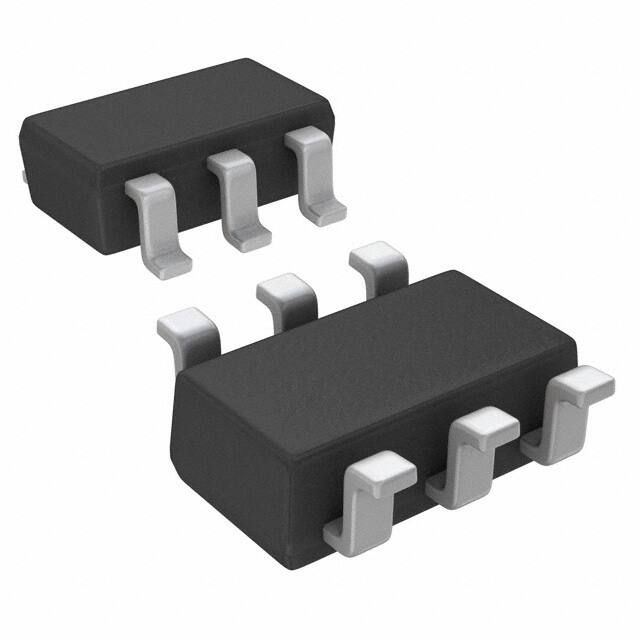
Manual Reset assertion in a small 6 Ld TSOT-23 package.
By connecting the three VSET pins to VDD, GND or floating,
users can program the voltage trip point from 1.60V to 2.85V
in 50mV increments on the ISL88016 and from 2.15V to
4.65V in 100mV increments on the ISL88017. These userselectable reset threshold voltages are accurate to ±2% over
temperature and the reset signal is valid down to 1V.
Intersil’s proprietary TwinPin™ combines the active low reset
out with the manual reset input into one pin. This provides
device adjustability without sacrificing functionality. These
parts are specifically designed for low power consumption
and high threshold accuracy.
Features
• Pin-Selectable Single Voltage Monitoring Supervisors
• User Pin-Selectable Voltage Trip Points
- ISL88016: 1.60V to 2.85V in 50mV Steps
- ISL88017: 2.15V to 4.65V in 100mV Steps
• Reduce Inventory on Fixed Voltage Trip Point Options
• Manual Reset Capability
• Proprietary TwinPin™ Combines Active-Low Reset Output
and Manual Reset Input Functions into One Pin
• Reset Signal Valid Down to VDD = 0.8V
• Voltage Threshold ±2% Accuracy Over Temp
• No External Components Necessary
• Immune to Power-Supply Transients
Pinout
• Ultra Low 3µA Supply Current
ISL88016, ISL88017
(6 LD TSOT-23)
TOP VIEW
VDD
GND
6
1
2
ISL88016
ISL88017
5
• Small 6 Ld TSOT-23 Pb-Free Plus Anneal Available
(RoHS Compliant)
RST/MR
VSET3
Ordering Information
PART NUMBER
(Note)
PART
TAPE &
MARKING REEL
PACKAGE
(Pb-Free)
PKG.
DWG. #
016Z
ISL88016IHTZ-T
(No longer available
or supported)
3k pcs 6 Ld TSOT-23 MDP0049
Tape & Reel
ISL88017IHTZ-T
017Z
3k pcs 6 Ld TSOT-23 MDP0049
Tape & Reel
• Process Control Systems
016Z
ISL88016IHTZ-TK
(No longer available
or supported)
1k pcs 6 Ld TSOT-23 MDP0049
Tape & Reel
• Intelligent Instruments
ISL88017IHTZ-T7A
017Z
250 pcs 6 Ld TSOT-23 MDP0049
Tape & Reel
ISL88017IHTZ-TK
017Z
1k pcs 6 Ld TSOT-23 MDP0049
Tape & Reel
VSET1
3
4
Applications
• Embedded Control Systems
• Computer Systems
VSET2
• Portable/Battery-Powered Equipment
ISL88016/17EVAL1Z Evaluation Platform
• PDA and Hand-Held PC Devices
NOTE: Intersil Pb-free plus anneal products employ special Pb-free
material sets; molding compounds/die attach materials and 100%
matte tin plate termination finish, which are RoHS compliant and
compatible with both SnPb and Pb-free soldering operations. Intersil
Pb-free products are MSL classified at Pb-free peak reflow
temperatures that meet or exceed the Pb-free requirements of
IPC/JEDEC J STD-020.
FN6141 Rev 1.00
August 5, 2015
Page 1 of 8
�ISL88016, ISL88017
Functional Block Diagrams
VDD
RST/MR
VSET1
VSET2
VOLTAGE
SETTING
POR
± VREF
PB
VDD
VSET3
GND
ISL88016
ISL88017
Product Features Table
FUNCTION
ISL88016
ISL88017
Active-Low Reset (RST)
x
x
Manual Reset Input (MR)
x
x
1.60V to 2.85V (50mV Increments) Pin-Selectable Voltage Trip Range
x
2.15V to 4.65V (100mV Increments) Pin-Selectable Voltage Trip Range
x
Pb-Free Package Option Available
x
x
Pin Descriptions
PIN
NAME
FUNCTION
1
VDD
Supply Voltage and Monitored Input. The VDD pin is the IC power supply terminal and also the
monitored input. The voltage at this pin is compared against the programmed voltage trip point, VTP.
A reset is first asserted when the device is initially powered up to ensure that the power supply has
stabilized. Thereafter, reset is again asserted whenever VDD falls below VTH. The device is designed
with hysteresis to help prevent chattering due to noise and is immune to brief power-supply transients.
2
GND
Ground.
3
VSET1
4
VSET2
5
VSET3
6
RST/MR
FN6141 Rev 1.00
August 5, 2015
Voltage Trip Point Select Pins 1, 2 and 3. These inputs are either tied either to GND or VDD or left
floating in various combinations to program the falling voltage trip point. See Voltage Trip Point Setting
Table on following page for programming configurations.
Proprietary TwinPin™ technology combines Active-Low Reset Output and Manual Reset Input
Functions into one pin. This dual function pin functions as both the reset output and a manual reset
input. The RST output pin has an integrated 100k pull-up resistor to VDD that is pulled to GND (LOW)
when reset is asserted, VDD < programmed voltage trip point. The MR input is an active-low
debounced input to which a user can connect a push-button to add manual reset capability.
Page 2 of 8
�ISL88016, ISL88017
Power-On Reset Voltage Setting
VTH
ISL88016
ISL88017
VSET1
VSET2
VSET3
1.60
2.15
GND
GND
GND
1.65
2.25
FLOAT
GND
GND
1.70
2.35
VDD
GND
GND
1.75
2.45
GND
FLOAT
GND
1.80
2.55
FLOAT
FLOAT
GND
1.85
2.65
VDD
FLOAT
GND
1.90
2.75
GND
VDD
GND
1.95
2.85
FLOAT
VDD
GND
2.00
2.95
VDD
VDD
GND
2.05
3.05
GND
GND
FLOAT
2.10
3.15
FLOAT
GND
FLOAT
2.15
3.25
VDD
GND
FLOAT
2.20
3.35
GND
FLOAT
FLOAT
2.25
3.45
FLOAT
FLOAT
FLOAT
2.30
3.55
VDD
FLOAT
FLOAT
2.35
3.65
GND
VDD
FLOAT
2.40
3.75
FLOAT
VDD
FLOAT
2.45
3.85
VDD
VDD
FLOAT
2.50
3.95
GND
GND
VDD
2.55
4.05
FLOAT
GND
VDD
2.60
4.15
VDD
GND
VDD
2.65
4.25
GND
FLOAT
VDD
2.70
4.35
FLOAT
FLOAT
VDD
2.75
4.45
VDD
FLOAT
VDD
2.80
4.55
GND
VDD
VDD
2.85
4.65
FLOAT
VDD
VDD
Reserved
Reserved
VDD
VDD
VDD
FN6141 Rev 1.00
August 5, 2015
Page 3 of 8
�ISL88016, ISL88017
Absolute Maximum Ratings
Recommended Operating Conditions
Temperature Under Bias . . . . . . . . . . . . . . . . . . . . .-40°C to +125°C
Storage Temperature . . . . . . . . . . . . . . . . . . . . . . .-65°C to +150°C
Voltage on Any Pin with Respect to GND . . . . . . . . . . . -1.0V to +7V
D.C. Output Current . . . . . . . . . . . . . . . . . . . . . . . . . . . . . . . . . . 5mA
Lead Temperature (Soldering, 10s) . . . . . . . . . . . . . . . . . . . . +300°C
Temperature Range (Industrial) . . . . . . . . . . . . . . . . .-40°C to +85°C
CAUTION: Absolute Maximum Ratings indicate limits beyond which permanent damage to the device and impaired reliability may occur. These are stress ratings
provided for information only and functional operation of the device at these or any other conditions beyond those indicated in the operational sections of this
specification are not implied.
For guaranteed specifications and test conditions, see Electrical Specifications. The guaranteed specifications apply only for the test conditions listed. Some
performance characteristics may degrade when the device is not operated under the listed test conditions.
Electrical Specifications
SYMBOL
Over the recommended operating conditions unless otherwise specified.
PARAMETER
TEST CONDITIONS
MIN
TYP
MAX
UNITS
5.5
V
BIAS
VDD
Supply Voltage Range
IDD
ISL88016 Supply Current
VDD > VTH
ISL88017 Supply Current
VDD > VTH
1.6
VDD = 5.0V
4.3
6
µA
VDD = 3.3V
3.1
4.9
µA
VDD = 2.5V
3.1
4.5
µA
VDD = 1.8V
2.5
4.4
µA
VDD = 5.0V
4.0
8.5
µA
VDD = 3.3V
3.2
8.5
µA
VDD = 2.5V
3.2
6.5
µA
VDD = 2.25V
3.0
5.4
µA
+2
%
VOLTAGE THRESHOLD
VTH
VDD Voltage Trip Point
VTHHYST
Hysteresis at VTH Input
Temperature = +25°C
See Power-On Reset Voltage
Setting Table on page 3
-2
1
%
RESET
ISL88016 Reset Output Voltage Low
VDD < VTH, Sinking 0.225mA
0.20
0.5
V
ISL88017 Reset Output Voltage Low
VDD < VTH, Sinking 0.225mA
0.20
0.5
V
VOH
Reset Output Voltage High
VDD VTH
VDD
tPOR
POR Time-Out Delay
tRST
VTH Low to Reset Asserted Delay
VOL
CLOAD
140
VDD Open
Load Capacitance on Reset Pin
200
V
280
ms
0.01
µs
5
pF
MANUAL RESET
VMR
MR Input Voltage
tMR
MR Minimum Pulse Width
RPU
Integrated RST/MR Pull-Up Resistor
100
10
mV
µs
100
k
VSET
IVSET
VSET Current
VVSET
VSET Open Pin Voltage
VIL
VSET Input Voltage Low
VIH
VSET Input Voltage High
FN6141 Rev 1.00
August 5, 2015
1
VSET = Open
µA
0.5VDD
V
0.1VDD
0.9 x VDD
V
V
Page 4 of 8
�ISL88016, ISL88017
VTH / VPOR
VDD
1V
tPOR
tRST
tPOR
tPOR
RST
MR
>tMR
FIGURE 1. VOLTAGE MONITORING TIMING DIAGRAM
Principles of Operation
The ISL88016 and ISL88017 devices provides a low cost
solution for those voltage monitoring applications needing
supply voltage supervision with power reset control, and
manual reset assertion. By integrating these common
features along with three pins of Vth programming into a
small 6 Ld TSOT-23 package and using only 1µA of supply
current, the ISL88016 and ISL88017 devices can lower
system cost, reduce board space requirements, and
increase the reliability of a system while reducing inventory
overhead costs.
Low Voltage Monitoring
During normal operation, the ISL88016 and ISL88017
monitor the voltage level of VDD. The device asserts a reset
(RST = LOW) if this voltage is less than the programmed
voltage trip point. The reset signal prevents system
operation during a power failure or brownout condition. This
reset signal remains asserted until VDD exceeds the voltage
threshold setting for the reset time delay period tPOR. (See
Figure 1).
The ISL88016 and ISL88017 allow users to customize the
Power-On Reset voltage threshold level, which is the voltage
at which the reset is deasserted. The three VSET inputs are
either tied to VDD, GND or left open to program VTH. See
the Power-On Reset Voltage Setting table on page 3 for
specific voltage configuration. Also see Figure 2 for a
schematic representation of the VSET pins being
programmed, noting the minimum necessary components
for IC operation. Do not attempt to reprogram a VTH while
the IC is biased.
FN6141 Rev 1.00
August 5, 2015
VDD
RST/MR
GND
ISL88016
ISL88017
VSET1
VSET3
VSET2
FIGURE 2. SETTING VPOR USING VSET INPUTS
Power-On Reset (POR)
Applying power to the ISL88016 and ISL88017 activates a
POR circuit which asserts reset once VDD = 1 V. (i.e., RST
goes LOW). This provides several benefits:
• It prevents the system microprocessor from starting to
operate with insufficient voltage.
• It prevents the processor from operating prior to
stabilization of the oscillator.
• It ensures that the monitored device is held out of
operation until internal registers are properly loaded.
• It allows time for an FPGA to download its configuration
prior to initialization of the circuit.
The reset signal remains asserted until VDD rises above the
minimum voltage sense level for time period tPOR. This
ensures that the VDD voltage has stabilized.
Optional VDD de-coupling capacitance can be added to filter
transients if needed.
Page 5 of 8
�ISL88016, ISL88017
Manual Reset
The manual reset input (MR) allows the user to trigger a
reset by using a push-button switch. The MR input is an
active low debounced input. By connecting a push-button
directly from MR to ground, the designer adds manual
system reset capability (see Figure 3). Reset is asserted if
the MR pin is pulled low to less than 100mV for 10µs or
longer while the push-button is closed. After MR is released,
the reset outputs remain asserted for tPOR (200ms) and then
released.
ISL88016
ISL88017
FIGURE 5. ISL88016/17EVAL1Z PHOTOGRAPH
RST/MR
0.1
TARGET 0%
PB
-0.1
88017_3.55V
FIGURE 3. CONNECTING A MANUAL RESET PUSH-BUTTON
VDD VTH (%)
88017_4.55V
Using the ISL88016/17EVAL1Z Platform
-0.5
-0.7
88016_2.25V
-0.9
88017_2.25V
-1.1
88016_1.75V
-1.3
-40
-30 -20
-10
0
10
25
35
45
55
65
75
85
(°C)
TEMPERATURE (oC)
FIGURE 6. SAMPLED VTH% TO TARGET OVER TEMP
6.00
BIAS CURRENT (uA)
The ISL88016/17EVAL1Z platform is provided with both an
ISL88016 in the top and an ISL88017 in the bottom
positions. Each IC is default programmed to VSET1, VSET2
and VSET3 = FLOAT but provided with jumpers to change
the Vth level by individually connecting the three VSET pins
to either VDD (1) or GND (0). To the left of the circuits is a
VSET programming table for easy reference. Provide
adequate bias to VDD to deassert RESET signal. See
Figure 4 for the ISL88016/17EVAL1Z schematic and
Figure 5 for its photograph.
88016_2.80V
-0.3
VDD = 5V
5.00
4.00
VDD = 2.5V
3.00
2.00
VDD = 1.8V
VDD = 3.3V
1.00
0.00
-40 -30
-20 -10
0
10
25
35
45
55
65
75
85
55
65
75
85
o
TEMPERATURE ( C)
tPOR (ms)
FIGURE 7. IDD OVER TEMP
FIGURE 4. ISL88016/17EVAL1Z SCHEMATIC
204
203
202
201
200
199
198
197
196
195
194
193
VDD = 5V
VDD = 3.3V
-40
-30
-20
-10
0
10
25
35
45
T EM P ERAT URE (o C)
FIGURE 8. tPOR OVER TEMP
FN6141 Rev 1.00
August 5, 2015
Page 6 of 8
�ISL88016, ISL88017
Revision History. The revision history provided is for informational purposes only and is believed to be accurate, but not
warranted. Please go to the web to make sure that you have the latest revision.
DATE
REVISION
CHANGE
August 5, 2015
FN6141.1
Updated Ordering Information Table on page 1.
Added Revision History and About Intersil sections.
Updated package outline drawing to latest revision. Changes from Revision A to Revision B are as follows:
Added dimensions (MILLIMETERS) to table.
About Intersil
Intersil Corporation is a leading provider of innovative power management and precision analog solutions. The company's products
address some of the largest markets within the industrial and infrastructure, mobile computing and high-end consumer markets.
For the most updated datasheet, application notes, related documentation and related parts, please see the respective product
information page found at www.intersil.com.
You may report errors or suggestions for improving this datasheet by visiting www.intersil.com/ask.
Reliability reports are also available from our website at www.intersil.com/support
FN6141 Rev 1.00
August 5, 2015
Page 7 of 8
�ISL88016, ISL88017
TSOT Package Family
MDP0049
e1
D
TSOT PACKAGE FAMILY
A
MILLIMETERS
6
N
SYMBOL
4
E1
2
E
3
0.15 C D
2X
1
5
2
(N/2)
0.25 C
2X N/2 TIPS
e
ddd M
B
C A-B D
b
NX
0.15 C A-B
1
3
D
2X
TSOT5
TSOT6
TSOT8
TOLERANCE
A
1.00
1.00
1.00
Max
A1
0.05
0.05
0.05
±0.05
A2
0.87
0.87
0.87
±0.03
b
0.38
0.38
0.29
±0.07
c
0.127
0.127
0.127
+0.07/-0.007
D
2.90
2.90
2.90
Basic
E
2.80
2.80
2.80
Basic
E1
1.60
1.60
1.60
Basic
e
0.95
0.95
0.65
Basic
e1
1.90
1.90
1.95
Basic
L
0.40
0.40
0.40
±0.10
L1
0.60
0.60
0.60
Reference
ddd
0.20
0.20
0.13
-
N
5
6
8
Reference
Rev. B 2/07
C
A2
SEATING
PLANE
1. Plastic or metal protrusions of 0.15mm maximum per side are
not included.
2. Plastic interlead protrusions of 0.15mm maximum per side are
not included.
A1
0.10 C
NOTES:
NX
3. This dimension is measured at Datum Plane “H”.
4. Dimensioning and tolerancing per ASME Y14.5M-1994.
(L1)
H
A
GAUGE
PLANE
c
5. Index area - Pin #1 I.D. will be located within the indicated zone
(TSOT6 AND TSOT8 only).
L
6. TSOT5 version has no center lead (shown as a dashed line).
0.25
4° ±4°
© Copyright Intersil Americas LLC 2006-2015. All Rights Reserved.
All trademarks and registered trademarks are the property of their respective owners.
For additional products, see www.intersil.com/en/products.html
Intersil products are manufactured, assembled and tested utilizing ISO9001 quality systems as noted
in the quality certifications found at www.intersil.com/en/support/qualandreliability.html
Intersil products are sold by description only. Intersil may modify the circuit design and/or specifications of products at any time without notice, provided that such
modification does not, in Intersil's sole judgment, affect the form, fit or function of the product. Accordingly, the reader is cautioned to verify that datasheets are
current before placing orders. Information furnished by Intersil is believed to be accurate and reliable. However, no responsibility is assumed by Intersil or its
subsidiaries for its use; nor for any infringements of patents or other rights of third parties which may result from its use. No license is granted by implication or
otherwise under any patent or patent rights of Intersil or its subsidiaries.
For information regarding Intersil Corporation and its products, see www.intersil.com
FN6141 Rev 1.00
August 5, 2015
Page 8 of 8
�


 工商网监
湘ICP备2023018690号
工商网监
湘ICP备2023018690号
