DATASHEET
ISL95310
FN8083
Rev 1.00
August 27, 2015
Digitally Controlled Potentiometer (XDCP™), Terminal Voltage 0V to 13.2V,
128 Taps Up/Down Interface
The Intersil ISL95310 is a digitally controlled potentiometer
(XDCP). The device consists of a resistor array, wiper
switches, a control section, and nonvolatile memory. The
wiper position is controlled by an Up/Down interface.
Features
The potentiometer is implemented by a resistor array
composed of 127 resistive elements and a wiper switching
network. Between each element and at either end are tap
points accessible to the wiper terminal. The wiper of each
potentiometer has an associated volatile Wiper Counter
Register (WR) and a non-volatile Initial Value Register (IVR)
that can be directly written to and read by the user. The
contents of the WR controls the position of the wiper on the
resistor array through the switches. At power-up, the device
recalls the contents of the default data registers to the
corresponding WR. The position of the wiper element is
controlled by the CS, U/D, and INC inputs. The position of
the wiper can be stored in nonvolatile memory and then be
recalled upon a subsequent power-up operation.
• DCP terminal voltage, 0 to +13.2V
The device can be used as a three-terminal potentiometer or
as a two-terminal variable resistor in a wide variety of
applications including:
• RTOTAL values = 10k50k
• LCD contrast control
• Non-volatile solid-state potentiometer
• Up/down interface with chip select enable
• 128 wiper tap points - 0.8% resolution
- Wiper position stored in nonvolatile memory and
recalled on power-up
• 127 resistive elements
- Temperature compensated
- Low wiper resistance 70 typical @ 3.3V
• Low power CMOS
- Standby current, 2µA at VCC = +3.6V
• High reliability
- Endurance, 200,000 data changes per bit
- Register data retention 50 years @ T 75°C
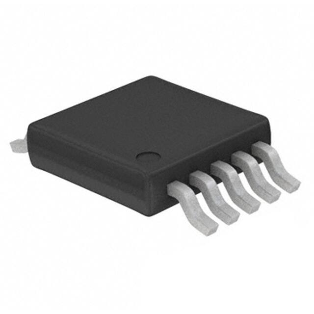
• 10-lead MSOP package
- Pb-free plus anneal available (RoHS compliant)
Pinout
• Parameter and bias adjustments
ISL95310
(10 LD MSOP)
TOP VIEW
• Mechanical potentiometer replacement
• Industrial and automotive control
Ordering Information
PART NUMBER
RESISTANCE
OPTION
()
TEMP
RANGE
(°C)
PACKAGE
(RoHS
Compliant)
ISL95310WIU10Z
(See Note) (No longer
available, recommended
replacement:
ISL95310UIU10Z-TK)
10K
-40 to +85 10 Ld MSOP
ISL95310UIU10Z
(See Note)
50K
-40 to +85 10 Ld MSOP
INC
U/D
1
10
GND
2
9
V+
VCC
3
8
RL
CS
4
7
RW
NC
5
6
RH
Add “-TK” suffix for tape and reel.
NOTE: Intersil Pb-free plus anneal products employ special Pb-free
material sets; molding compounds/die attach materials and 100%
matte tin plate termination finish, which are RoHS compliant and
compatible with both SnPb and Pb-free soldering operations. Intersil
Pb-free products are MSL classified at Pb-free peak reflow
temperatures that meet or exceed the Pb-free requirements of
IPC/JEDEC J STD-020.
FN8083 Rev 1.00
August 27, 2015
Page 1 of 9
�ISL95310
Block Diagram
U/D
INC
V+
VCC
CS
Up/Down
7-BIT
UP/DOWN
COUNTER
126
125
RH
(U/D)
Increment
CONTROL
AND
MEMORY
(INC)
Device Select
RW
(CS)
RH
127
7-BIT
NONVOLATILE
MEMORY
124
ONE
OF
128
TRANSFER
GATES
RESISTOR
ARRAY
DECODER
RL
2
STORE AND
RECALL
CONTROL
CIRCUITRY
GND
SIMPLE BLOCK DIAGRAM
1
0
RL
RW
DETAILED BLOCK DIAGRAM
Pin Descriptions
PIN NUMBER
SYMBOL
DESCRIPTION
1
U/D
Controls the direction of wiper movement and whether the counter is incremented or decremented
2
GND
Ground
3
VCC
Positive logic supply voltage
4
CS
Chip select; the device is selected when the CS input is LOW; also used to initiate a nonvolatile store
5
NC
No connect; pin is to be left unconnected
6
RH
A fixed terminal for one end of the potentiometer resistor
7
RW
The wiper terminal which is equivalent to the movable terminal of a potentiometer
8
RL
A fixed terminal for one end of the potentiometer resistor
9
V+
Positive bias voltage for the potentiometer wiper control
10
INC
Increment input; negative edge triggered
FN8083 Rev 1.00
August 27, 2015
Page 2 of 9
�ISL95310
Absolute Maximum Ratings
Recommended Operating Conditions
Storage temperature . . . . . . . . . . . . . . . . . . . . . . . .-65°C to +150°C
Voltage on CS, INC, U/D
with respect to GND . . . . . . . . . . . . . . . . . . . . -0.3V to VCC +0.3V
Voltage on V+ (referenced to GND) . . . . . . . . . . . . . . . . . . . . +13.2V
V = |V(RH)-V(RL)| . . . . . . . . . . . . . . . . . . . . . . . . . . . . . . . . . . . . .V+
RH, RL, RW . . . . . . . . . . . . . . . . . . . . . . . . . . . . . . . . . . . . . . . . . .V+
Lead temperature (soldering 10s) . . . . . . . . . . . . . . . . . . . . . +300°C
IW (10s) . . . . . . . . . . . . . . . . . . . . . . . . . . . . . . . . . . . . . . . . . . ±6mA
VCC . . . . . . . . . . . . . . . . . . . . . . . . . . . . . . . . . . . . . . . . -0.3V to +6V
Power rating of each DCP . . . . . . . . . . . . . . . . . . . . . . . . . . . .20mW
Temperature Range (Industrial) . . . . . . . . . . . . . . . . .-40°C to +85°C
VCC . . . . . . . . . . . . . . . . . . . . . . . . . . . . . . . . . . . . . . . . 2.7V to 5.5V
V+ . . . . . . . . . . . . . . . . . . . . . . . . . . . . . . . . . . . . . . . . 8.0V to 13.2V
Wiper current of each DCP . . . . . . . . . . . . . . . . . . . . . . . . . . ±3.0mA
CAUTION: Stresses above those listed under “Absolute Maximum Ratings” may cause permanent damage to the device. This is a stress rating only; functional
operation of the device (at these or any other conditions above those listed in the operational sections of this specification) is not implied. Exposure to absolute
maximum rating conditions for extended periods may affect device reliability.
Analog Specifications Over recommended operating conditions unless otherwise stated.
SYMBOL
RTOTAL
PARAMETER
RH to RL resistance
TEST CONDITIONS
UNIT
k
U option
50
k
RH terminal voltage
VRL = 0V
RW
Wiper resistance
V+ = 12V, wiper current = V+ / RTOTAL
-20
+20
%
0
V+
V
200
70
Potentiometer Capacitance (Note 13)
Leakage on DCP pins
MAX
10
VRH
ILkgDCP
TYP
(Note 1)
W option
RH to RL resistance tolerance
CH/CL/CW
MIN
10/10/
25
Voltage at pin from GND to V+
pF
0.1
1
µA
-1
1
LSB
(Note 2)
W option
-0.75
0.75
U option
-0.5
0.5
LSB
(Note 2)
U option
0
1
7
W option
0
0.5
2
U option
-7
-1
0
W option
-2
-1
0
VOLTAGE DIVIDER MODE (0V @ RL; V+ @ RH; measured at RW, unloaded)
INL
(Note 6)
Integral non-linearity
DNL
(Note 5)
Differential non-linearity
ZSerror
(Note 3)
Zero-scale error
FSerror
(Note 4)
Full-scale error
TCV (Note 7) Ratiometric Temperature Coefficient
DCP register set to 40 hex
±4
LSB
(Note 2)
LSB
(Note 2)
ppm/°C
RESISTOR MODE (Measurements between RW and RL with RH not connected, or between RW and RH with RL not connected)
RINL
(Note 11)
Integral non-linearity
DCP register set between 20 hex and 7F hex;
monotonic over all tap positions
RDNL
(Note 10)
Differential non-linearity
Roffset
(Note 9)
Offset
TCR
(Note 12)
Resistance Temperature Coefficient
FN8083 Rev 1.00
August 27, 2015
-1
1
MI
(Note 8)
W option
-0.75
0.75
U option
-0.5
0.5
MI
(Note 8)
DCP Register set to 00 hex, W option
0
1
7
MI
(Note 8)
DCP Register set to 00 hex, U option
0
0.5
2
MI
(Note 8)
DCP register set between 20 hex and 7F hex
±45
ppm/°C
Page 3 of 9
�ISL95310
Operating Specifications Over the recommended operating conditions unless otherwise specified.
SYMBOL
PARAMETER
TEST CONDITIONS
MIN
TYP
(Note 1)
MAX
UNIT
ICC1
VCC supply current, volatile write/read CS = VIL, U/D = VIL or VIH and INC = 0.4V/2.4V
min; tCYC RL, RH, RW not connected
1
mA
ICC2
VCC supply current, nonvolatile write
CS = VIL, U/D = VIL or VIH and INC = 0.4V/2.4V
min; tCYC RL, RH, RW not connected
3
mA
VCC current, standby
VCC = +5.5V, 2-wire interface in standby state
5
µA
VCC = +3.6V, 2-wire interface in standby state
2
µA
V+ bias current
V+ = 13.2V; VCC = +5.5V
1
µA
Leakage current, at pins INC, CS,
U/D, A0, and A1 pins
Voltage at pin from GND to VCC
10
µA
CS input leakage current
VIN = VCC
±1
µA
ISB
IV+
ILkgDig
ILI
IV+
-10
VCC = 3V, CS = 0
60
100
150
µA
VCC = 5V, CS = 0
120
200
250
µA
V+ bias current
V+ = 13.2V; VCC = +5.5V
1
µA
tDCP
(Note 13)
DCP wiper response time
INC falling edge of last bit of DCP data byte to
wiper change
1
µs
Vpor
(Note 13)
Power-on recall voltage
Minimum VCC at which memory recall occurs
2.6
V
VCC Ramp
(Note 13)
VCC ramp rate
tD
(Note 13)
Power up delay
1.8
0.2
V/ms
3
VCC above Vpor, to DCP initial value register
recall completed, and 2-wire Interface in standby
state
ms
EEPROM SPECS
EEPROM endurance
Temperature 75°C
EEPROM retention
150,000
Cycles
50
Years
SERIAL INTERFACE SPECS
VIL
INC, CS, and U/D
-0.3
0.3*
VCC
V
VIH
INC, CS, and U/D
0.7*
VCC
VCC+
0.3
V
Hysteresis
(Note 13)
INC, CS, and U/D input buffer
hysteresis
0.05*
VCC
Cpin
(Note 13)
INC, CS, and U/D pin capacitance
AC Electrical Specifications
10
pF
VCC = 5V ±10%, TA = Full Operating Temperature Range unless otherwise stated
SYMBOL
tCl
V
PARAMETER
MIN
TYP
(Note 4)
MAX
UNIT
CS to INC setup
100
ns
tlD (Note 13)
INC HIGH to U/D change
100
ns
tDI (Note 13)
U/D to INC setup
1
µs
tlL
INC LOW period
1
µs
tlH
INC HIGH period
1
µs
tlC
INC inactive to CS inactive
1
µs
FN8083 Rev 1.00
August 27, 2015
Page 4 of 9
�ISL95310
AC Electrical Specifications
VCC = 5V ±10%, TA = Full Operating Temperature Range unless otherwise stated (Continued)
SYMBOL
tCPHS
tCPHNS (Note 13)
tIW (Note 13)
tCYC
tR, tF (Note 13)
PARAMETER
MIN
TYP
(Note 4)
MAX
UNIT
CS deselect time (STORE)
20
ms
CS deselect time (NO STORE)
1
µs
INC to RW change
100
INC cycle time
500
4
INC input rise and fall time
µs
µs
500
µs
NOTES:
1. Typical values are for TA = 25°C and 3.3V supply voltage.
2. LSB: [V(RW)127 – V(RW)0]/127. V(RW)127 and V(RW)0 are V(RW) for the DCP register set to 7F hex and 00 hex respectively. LSB is the
incremental voltage when changing from one tap to an adjacent tap.
3. ZS error = V(RW)0 /LSB.
4. FS error = [V(RW)127 – V+]/LSB.
5. DNL = [V(RW)i – V(RW)i-1]/LSB-1, for i = 1 to 127. i is the DCP register setting.
6. INL = V(RW)i – (i • LSB – V(RW)0) for i = 1 to 127.
Max V RW i – Min V RW i
10 6
7. TC V = ------------------------------------------------------------------------------------------------- x ---------------- Max V RW i + Min V RW i § 2 125°C
for i = 16 to 120 decimal, T = -40°C to 85°C. Max( ) is the maximum value of the wiper voltage and Min ( ) is the minimum value of the wiper
voltage over the temperature range.
8. MI = |R127 – R0| /127. R127 and R0 are the measured resistances for the DCP register set to 7F hex and 00 hex respectively.
9. Roffset = R0/MI, when measuring between RW and RL.
Roffset = R127/MI, when measuring between RW and RH.
10. RDNL = (Ri – Ri-1)/MI, for i = 16 to 127.
11. RINL = [Ri – (MI • i) – R0]/MI, for i = 16 to 127.
6
Max Ri – Min Ri
10
12. TC = ------------------------------------------------------------------ ----------------R
Max Ri + Min Ri § 2 125°C
for i = 16 to 127, T = -40°C to 85°C. Max( ) is the maximum value of the resistance and Min ( ) is the minimum value of the resistance over the
temperature range.
13. This parameter is not 100% tested.
14. tWC is the minimum cycle time to be allowed for any non-volatile Write by the user, unless Acknowledge Polling is used. It is the time from a
valid STOP condition at the end of a Write sequence of a 3-wire serial interface Write operation, to the end of the self-timed internal non-volatile
write cycle.
Symbol Table
WAVEFORM
FN8083 Rev 1.00
August 27, 2015
INPUTS
OUTPUTS
Must be steady
Will be steady
May change from Low to High
Will change from Low to High
May change from High to Low
Will change from High to Low
Don’t Care: Changes Allowed
Changing: State Not Known
N/A
Center Line is High Impedance
Page 5 of 9
�ISL95310
A.C. Timing
CS
tCYC
tCI
tIL
tIH
tCPHNS
tCPHS
tIC
90%
INC
90%
10%
tID
tDI
tF
tR
U/D
tIW
RW
MI
(3)
Power Up and Down Requirements
In order to prevent unwanted tap position changes, or an
inadvertent store, bring the CS and INC high before or
concurrently with the VCC pin on power-up. The
potentiometer voltages must be applied after this sequence
is completed. During power-up, the data sheet parameters
for the DCP do not fully apply until 1ms after VCC reaches its
final value. The VCC ramp spec is always in effect.
Pin Descriptions
RH and RL
The high (RH) and low (RL) terminals of the ISL95310 are
equivalent to the fixed terminals of a mechanical
potentiometer. The terminology of RL and RH references the
relative position of the terminal in relation to wiper movement
direction selected by the U/D input and not the voltage
potential on the terminal.
RW
RW is the wiper terminal and is equivalent to the movable
terminal of a mechanical potentiometer. The position of the
wiper within the array is determined by the control inputs.
Up/Down (U/D)
The U/D input controls the direction of the wiper movement
and whether the counter is decremented.
Increment (INC)
The INC input is negative-edge triggered. Toggling INC will
move the wiper and either increment or decrement the
counter in the direction indicated by the logic level on the
U/D input.
Chip Select (CS)
CS is returned HIGH while the INC input is also HIGH. After
the store operation is complete the ISL95310 will be placed
in the low power standby mode until the device is selected
once again.
Principles of Operation
There are three sections of the ISL95310: the input control,
counter and decode section; the nonvolatile memory; and
the resistor array. The input control section operates just like
an up/down counter. The output of this counter is decoded to
turn on a single electronic switch connecting a point on the
resistor array to the wiper output. Under the proper
conditions the contents of the counter can be stored in
nonvolatile memory and retained for future use. The resistor
array is comprised of 127 individual resistors connected in
series. At either end of the array and between each resistor
is an electronic switch that transfers the potential at that
point to the wiper.
The wiper, when at either fixed terminal, acts like its
mechanical equivalent and does not move beyond the last
position. That is, the counter does not wrap around when
clocked to either extreme.
The electronic switches on the device operate in a “make
before break” mode when the wiper changes tap positions. If
the wiper is moved several positions, multiple taps are
connected to the wiper for tIW (INC to VW change). The
RTOTAL value for the device can temporarily be reduced by
a significant amount if the wiper is moved several positions.
When the device is powered-down, the last wiper position
stored will be maintained in the nonvolatile memory. When
power is restored, the contents of the memory are recalled
and the wiper is set to the value last stored.
The device is selected when the CS input is LOW. The
current counter value is stored in nonvolatile memory when
FN8083 Rev 1.00
August 27, 2015
Page 6 of 9
�ISL95310
On applying power to the ISL95310, the VCC supply should
have a monotonic ramp to the specified operating voltage. It
is important that once VCC reaches 1V that it increases to at
least 2.5V in less than 7.5ms (0.2V/ms). The ramp rate
before and after these thresholds is not important.
VCC must be applied prior to, or simultaneously, with V+.
Under no condition should V+ be applied without VCC. While
the sequence of applying V+ and VCC to the ISL95310 does
not affect the proper recall of the wiper position, applying V+
before VCC powers the electronic switches of the DCP
before the electronic switch control signals are applied. This
can result in multiple electronic switches being turned on,
which could load the power supply and cause brief,
unexpected potentiometer wiper settings.
To prevent unknown wiper positions on the ISL95310 on
power down, it is recommended that V+ turn off before or
simultaneously with VCC. If V+ remains on after VCC turns
off, the wiper position can remain unchanged from its
previous setting or it can go to an undefined state.
TABLE 1. MODE SELECTION
CS
INC
U/D
MODE
L
H
Wiper up
L
L
Wiper down
H
X
Store wiper position
X
X
Standby current
L
X
No store, return to standby
H
X
Standby
L
H
Wiper up one position
(not recommended)
L
L
Wiper down one position
(not recommended)
H
H
Instructions and Programming
The INC, U/D and CS inputs control the movement of the
wiper along the resistor array. With CS set LOW the device
is selected and enabled to respond to the U/D and INC
inputs. HIGH to LOW transitions on INC will increment or
decrement (depending on the state of the U/D input) a seven
bit counter. The output of this counter is decoded to select
one of one hundred wiper positions along the resistive array.
The value of the counter is stored in nonvolatile memory
whenever CS transitions HIGH while the INC input is also
HIGH.
The system may select the ISL95310, move the wiper and
deselect the device without having to store the latest wiper
position in nonvolatile memory. After the wiper movement is
performed as described above and once the new position is
reached, the system must keep INC LOW while taking CS
HIGH. The new wiper position will be maintained until
changed by the system or until a power-up/down cycle
recalled the previously stored data.
This procedure allows the system to always power-up to a
preset value stored in nonvolatile memory; then during
system operation minor adjustments could be made. The
adjustments might be based on user preference, system
parameter changes due to temperature drift, etc.
The state of U/D may be changed while CS remains LOW.
This allows the host system to enable the device and then
move the wiper up and down until the proper trim is attained.
During initial power-up CS must go high along with or before
VCC to avoid an accidental store generation.
FN8083 Rev 1.00
August 27, 2015
Page 7 of 9
�ISL95310
Revision History
The revision history provided is for informational purposes only and is believed to be accurate, but not warranted. Please go to the web to make
sure that you have the latest revision.
DATE
REVISION
August 27, 2015
FN8083.1
CHANGE
- Ordering Information Table on page 1.
- Added Revision History.
- Added About Intersil Verbiage.
-Updated POD M10.118 to most current version change is as follows:
Added land pattern.
About Intersil
Intersil Corporation is a leading provider of innovative power management and precision analog solutions. The company's products
address some of the largest markets within the industrial and infrastructure, mobile computing and high-end consumer markets.
For the most updated datasheet, application notes, related documentation and related parts, please see the respective product
information page found at www.intersil.com.
You may report errors or suggestions for improving this datasheet by visiting www.intersil.com/ask.
Reliability reports are also available from our website at www.intersil.com/support
© Copyright Intersil Americas LLC 2005-2015. All Rights Reserved.
All trademarks and registered trademarks are the property of their respective owners.
For additional products, see www.intersil.com/en/products.html
Intersil products are manufactured, assembled and tested utilizing ISO9001 quality systems as noted
in the quality certifications found at www.intersil.com/en/support/qualandreliability.html
Intersil products are sold by description only. Intersil may modify the circuit design and/or specifications of products at any time without notice, provided that such
modification does not, in Intersil's sole judgment, affect the form, fit or function of the product. Accordingly, the reader is cautioned to verify that datasheets are
current before placing orders. Information furnished by Intersil is believed to be accurate and reliable. However, no responsibility is assumed by Intersil or its
subsidiaries for its use; nor for any infringements of patents or other rights of third parties which may result from its use. No license is granted by implication or
otherwise under any patent or patent rights of Intersil or its subsidiaries.
For information regarding Intersil Corporation and its products, see www.intersil.com
FN8083 Rev 1.00
August 27, 2015
Page 8 of 9
�ISL95310
Package Outline Drawing
M10.118
10 LEAD MINI SMALL OUTLINE PLASTIC PACKAGE
Rev 1, 4/12
5
3.0±0.05
A
DETAIL "X"
D
10
1.10 MAX
SIDE VIEW 2
0.09 - 0.20
4.9±0.15
3.0±0.05
5
0.95 REF
PIN# 1 ID
1
2
0.50 BSC
B
GAUGE
PLANE
TOP VIEW
0.55 ± 0.15
0.25
3°±3°
0.85±010
H
DETAIL "X"
C
SEATING PLANE
0.18 - 0.27
0.08 M C A-B D
0.10 ± 0.05
0.10 C
SIDE VIEW 1
(5.80)
NOTES:
(4.40)
(3.00)
1. Dimensions are in millimeters.
2. Dimensioning and tolerancing conform to JEDEC MO-187-BA
and AMSEY14.5m-1994.
3. Plastic or metal protrusions of 0.15mm max per side are not
included.
4. Plastic interlead protrusions of 0.15mm max per side are not
included.
(0.50)
(0.29)
(1.40)
5. Dimensions are measured at Datum Plane "H".
6. Dimensions in ( ) are for reference only.
TYPICAL RECOMMENDED LAND PATTERN
FN8083 Rev 1.00
August 27, 2015
Page 9 of 9
�


 工商网监
湘ICP备2023018690号
工商网监
湘ICP备2023018690号
