DATASHEET
ISLA214S50
FN7973
Rev 2.00
April 25, 2013
14-Bit, 500/350 MSPS JESD204B High Speed Serial Output ADC
The ISLA214S50 is a series of low-power, high-performance,
14-bit, analog-to-digital converters. Designed with
FemtoCharge™ technology on a standard CMOS process, the
series supports sampling rates of up to 500MSPS. The
ISLA214S50 is part of a pin-compatible family of 12-, 14-, and
16-bit A/Ds with maximum sample rates ranging from
125MSPS to 500MSPS. The family minimizes power
consumption while providing state-of-the-art dynamic
performance.
The device utilizes two time-interleaved 250MSPS unit ADCs to
achieve the ultimate sample rate of 500MSPS. A single
500MHz conversion clock is presented to the converter, and all
interleave clocking is managed internally. The proprietary
Intersil Interleave Engine (I2E) performs automatic correction
of offset, gain, and sample time mismatches between the unit
ADCs to optimize performance.
The ISLA214S50 offers a highly configurable, JESD204Bcompliant, high speed serial output link. The link offers data
rates up to 4.375 Gbps per lane and multiple packing modes.
The link can be configured to use two or three lanes to
transmit the conversion data, allowing for flexibility in the
receiver design. The JESD204 transmitter also provides
deterministic latency and multi-chip time alignment support to
satisfy complex synchronization requirements.
A serial peripheral interface (SPI) port allows for extensive
configurability of the ADC and its JESD204B transmitter
including access to its built-in link and transport-layer test
patterns as well as the programmable clock divider, enabling
2x harmonic clocking.
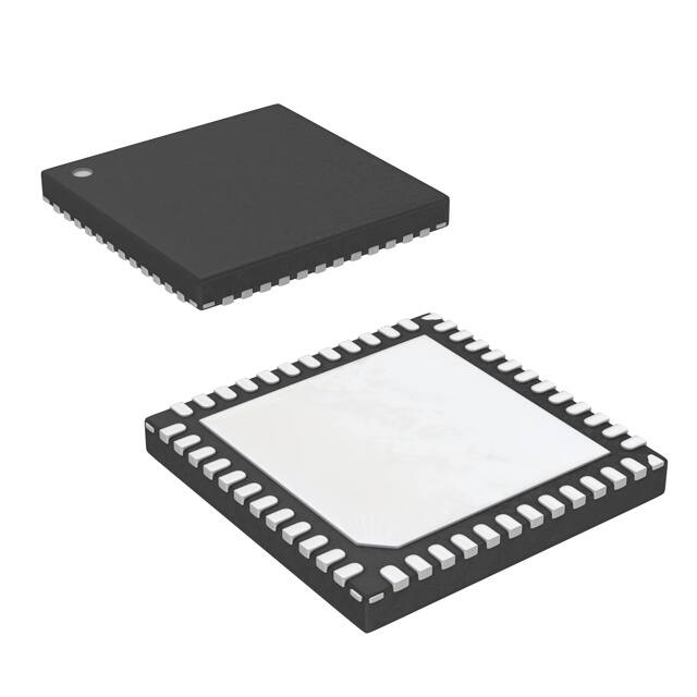
The ISLA214S50 is available in a space-saving 7mmx7mm 48
Ld QFN package. The package features a thermal pad for
improved thermal performance and is specified over the full
industrial temperature range (-40°C to +85°C)
Features
• JESD204A/B High Speed Data Interface
- JESD204A Compliant
- JESD204B Device Subclass 0 Compliant
- JESD204B Device Subclass 2 Compatible
- Up to 3 JESD204 Output Lanes Running up to 4.375Gbps
- Highly Configurable JESD204 Transmitter
• Multiple Chip Time Alignment and Deterministic Latency
Support (JESD204B Device Subclass 2)
• SPI Programmable Debugging Features and Test Patterns
• 48-pin QFN 7mmx7mm Package
Key Specifications
• SNR @ 500/350MSPS
73.1/74.1 dBFS fIN = 30MHz
71.0/71.6 dBFS fIN = 363MHz
• SFDR @ 500/350MSPS
87/87 dBc fIN = 30MHz
78/81 dBc fIN = 363MHz
• Total Power Consumption: 1060mW @ 500MSPS
Applications
•
•
•
•
•
Radar and Satellite Antenna Array Processing
Broadband Communications and Microwave Receivers
High-Performance Data Acquisition
Communications Test Equipment
High-Speed Medical Imaging
Pin-Compatible Family
RESOLUTION
SPEED
(MSPS)
PRODUCT
AVAILABILITY
ISLA214S50
14
500
Now
ISLA214S35
14
350
Soon
MODEL
+
FIGURE 1. SERDES DATA EYE AT 4.375Gbps
FN7973 Rev 2.00
April 25, 2013
Page 1 of 41
�CLKP
OVDD
OVDD
(PLL)
SYNC
AVDD
ISLA214S50
CLOCK
GENERATION
CLKN
AINP
14-BIT
250MSPS
ADC
SHA
AINN
LANE[2:0]P
LANE[2:0]N
VREF
VCM
I2E
AND
JESD204
TRANSMITTER
14-BIT
250MSPS
ADC
VREF
+
–
OVSS
CSB
SCLK
SDIO
SDO
SPI
CONTROL
RESETN
AVSS
(PLL)
NAPSLP
AVSS
1.25V
FIGURE 2. BLOCK DIAGRAM
Pin Configuration
FN7973 Rev 2.00
April 25, 2013
DNC
DNC
AVDD
NAPSLP
CLKDIV
SDIO
SCLK
CSB
SDO
OVDD
OVSS
OVSS
ISLA214S50
(48 LD QFN)
TOP VIEW
48
47
46
45
44
43
42
41
40
39
38
37
VCM
1
36 OVDD
AVDD
2
35 OVSS
AVSS
3
34 LANE2N
AVSS
4
33 LANE2P
VINN
5
32 OVSS
VINN
6
31 LANE1N
VINP
7
30 LANE1P
VINP
8
29 OVSS
AVSS
9
28 LANE0N
AVSS
10
27 LANE0P
AVDD
11
DNC
12
26 OVSS
PAD – Exposed Paddle
13
14
15
16
17
18
19
20
21
22
23
24
RESETN
AVDD
AVDD
CLKP
CLKN
SYNCP
SYNCN
DNC
OVSS (PLL)
OVDD (PLL)
OVSS (PLL)
OVDD (PLL)
25 OVDD
Page 2 of 41
�ISLA214S50
Pin Descriptions
PIN NUMBER
NAME
FUNCTION
2, 11, 14, 15, 46
AVDD
1.8V Analog Supply
12, 20, 47, 48
DNC
Do Not Connect
3, 4, 9, 10
AVSS
Analog Ground
7, 8
VINP
Analog Input Positive
5, 6
VINN
Analog Input Negative
1
VCM
Common Mode Output
44
CLKDIV
16, 17
CLKP, CLKN
45
NAPSLP
Power Control (Nap, Sleep modes)
13
RESETN
Power On Reset (Active Low)
26, 29, 32, 35, 37, 38
OVSS
Output Ground
25, 36, 39
OVDD
1.8V Digital Supply
22, 24
OVDD (PLL)
1.8V Analog Supply for SERDES PLL
21, 23
OVSS (PLL)
Analog Ground Supply for SERDES PLL
18, 19
SYNCP, SYNCN
27, 28
LANE0P, LANE0N
SERDES Lane 0
30, 31
LANE1P, LANE1N
SERDES Lane 1
33, 34
LANE2P, LANE2N
SERDES Lane 2
40
SDO
SPI Serial Data Output
41
CSB
SPI Chip Select (active low)
42
SCLK
SPI Clock
43
SDIO
SPI Serial Data Input/Output
PAD
AVSS
Exposed Paddle. Analog Ground (connect to AVSS)
Clock Divider Control
Clock Input True, Complement
JESD204 SYNC Input
Ordering Information
PART NUMBER
(Notes 1, 2)
PART
MARKING
TEMP. RANGE
(°C)
PACKAGE
(Pb-free)
PKG.
DWG. #
ISLA214S50IR1Z
ISLA214S50 IR1Z
-40 to +85
48 Ld QFN
L48.7x7G
Coming Soon
ISLA214S35IR1Z
ISLA214S35 IR1Z
-40 to +85
48 Ld QFN
L48.7x7G
Coming Soon
ISLA214S50IR48EV1Z
Evaluation Board
NOTES:
1. These Intersil Pb-free plastic packaged products employ special Pb-free material sets; molding compounds/die attach materials and NiPdAu plate-e4
termination finish, which is RoHS compliant and compatible with both SnPb and Pb-free soldering operations. Intersil Pb-free products are MSL
classified at Pb-free peak reflow temperatures that meet or exceed the Pb-free requirements of IPC/JEDEC J STD-020.
2. For Moisture Sensitivity Level (MSL), please see device information page for ISLA214S50, ISLA214S35. For more information on MSL please see
techbrief TB363.
FN7973 Rev 2.00
April 25, 2013
Page 3 of 41
�ISLA214S50
Table of Contents
Absolute Maximum Ratings . . . . . . . . . . . . . . . . . . . . . . . . . . . . . . . . . . . . . . . . . . . . . . . . . . . . . . . . . . . . . . . . . . . . . . . . . . . . . . . . . . . 5
Thermal Information . . . . . . . . . . . . . . . . . . . . . . . . . . . . . . . . . . . . . . . . . . . . . . . . . . . . . . . . . . . . . . . . . . . . . . . . . . . . . . . . . . . . . . . . . 5
Recommended Operating Conditions . . . . . . . . . . . . . . . . . . . . . . . . . . . . . . . . . . . . . . . . . . . . . . . . . . . . . . . . . . . . . . . . . . . . . . . . . . 5
Electrical Specifications . . . . . . . . . . . . . . . . . . . . . . . . . . . . . . . . . . . . . . . . . . . . . . . . . . . . . . . . . . . . . . . . . . . . . . . . . . . . . . . . . . . . . 5
I2E Specifications . . . . . . . . . . . . . . . . . . . . . . . . . . . . . . . . . . . . . . . . . . . . . . . . . . . . . . . . . . . . . . . . . . . . . . . . . . . . . . . . . . . . . . . . . . . 7
Digital Specifications . . . . . . . . . . . . . . . . . . . . . . . . . . . . . . . . . . . . . . . . . . . . . . . . . . . . . . . . . . . . . . . . . . . . . . . . . . . . . . . . . . . . . . . . 8
Switching Specifications . . . . . . . . . . . . . . . . . . . . . . . . . . . . . . . . . . . . . . . . . . . . . . . . . . . . . . . . . . . . . . . . . . . . . . . . . . . . . . . . . . . . . 9
Typical Performance Curves . . . . . . . . . . . . . . . . . . . . . . . . . . . . . . . . . . . . . . . . . . . . . . . . . . . . . . . . . . . . . . . . . . . . . . . . . . . . . . . . . 10
Theory of Operation. . . . . . . . . . . . . . . . . . . . . . . . . . . . . . . . . . . . . . . . . . . . . . . . . . . . . . . . . . . . . . . . . . . . . . . . . . . . . . . . . . . . . . . . . 15
Functional Description . . . . . . . . . . . . . . . . . . . . . . . . . . . . . . . . . . . . . . . . . . . . . . . . . . . . . . . . . . . . . . . . . . . . . . . . . . . . . . . . . . . . . . . . . . . 15
Power-On Calibration. . . . . . . . . . . . . . . . . . . . . . . . . . . . . . . . . . . . . . . . . . . . . . . . . . . . . . . . . . . . . . . . . . . . . . . . . . . . . . . . . . . . . . . . . . . . . 15
User Initiated Reset . . . . . . . . . . . . . . . . . . . . . . . . . . . . . . . . . . . . . . . . . . . . . . . . . . . . . . . . . . . . . . . . . . . . . . . . . . . . . . . . . . . . . . . . . . . . . . 16
Temperature Calibration. . . . . . . . . . . . . . . . . . . . . . . . . . . . . . . . . . . . . . . . . . . . . . . . . . . . . . . . . . . . . . . . . . . . . . . . . . . . . . . . . . . . . 16
Analog Input . . . . . . . . . . . . . . . . . . . . . . . . . . . . . . . . . . . . . . . . . . . . . . . . . . . . . . . . . . . . . . . . . . . . . . . . . . . . . . . . . . . . . . . . . . . . . . . . . . . . 17
Clock Input . . . . . . . . . . . . . . . . . . . . . . . . . . . . . . . . . . . . . . . . . . . . . . . . . . . . . . . . . . . . . . . . . . . . . . . . . . . . . . . . . . . . . . . . . . . . . . . . . . . . . 18
Jitter. . . . . . . . . . . . . . . . . . . . . . . . . . . . . . . . . . . . . . . . . . . . . . . . . . . . . . . . . . . . . . . . . . . . . . . . . . . . . . . . . . . . . . . . . . . . . . . . . . . . . . . . . . . 18
Voltage Reference . . . . . . . . . . . . . . . . . . . . . . . . . . . . . . . . . . . . . . . . . . . . . . . . . . . . . . . . . . . . . . . . . . . . . . . . . . . . . . . . . . . . . . . . . . . . . . . 18
Digital Outputs . . . . . . . . . . . . . . . . . . . . . . . . . . . . . . . . . . . . . . . . . . . . . . . . . . . . . . . . . . . . . . . . . . . . . . . . . . . . . . . . . . . . . . . . . . . . . . . . . . 18
Power Dissipation . . . . . . . . . . . . . . . . . . . . . . . . . . . . . . . . . . . . . . . . . . . . . . . . . . . . . . . . . . . . . . . . . . . . . . . . . . . . . . . . . . . . . . . . . . . . . . . 18
Nap/Sleep. . . . . . . . . . . . . . . . . . . . . . . . . . . . . . . . . . . . . . . . . . . . . . . . . . . . . . . . . . . . . . . . . . . . . . . . . . . . . . . . . . . . . . . . . . . . . . . . . . . . . . 19
Data Format . . . . . . . . . . . . . . . . . . . . . . . . . . . . . . . . . . . . . . . . . . . . . . . . . . . . . . . . . . . . . . . . . . . . . . . . . . . . . . . . . . . . . . . . . . . . . . . . . . . . 19
I2E Requirements and Restrictions . . . . . . . . . . . . . . . . . . . . . . . . . . . . . . . . . . . . . . . . . . . . . . . . . . . . . . . . . . . . . . . . . . . . . . . . . . . 20
Overview . . . . . . . . . . . . . . . . . . . . . . . . . . . . . . . . . . . . . . . . . . . . . . . . . . . . . . . . . . . . . . . . . . . . . . . . . . . . . . . . . . . . . . . . . . . . . . . . . . . . . . . . . . . . 20
Active Run State . . . . . . . . . . . . . . . . . . . . . . . . . . . . . . . . . . . . . . . . . . . . . . . . . . . . . . . . . . . . . . . . . . . . . . . . . . . . . . . . . . . . . . . . . . . . . . . . 20
Power Meter . . . . . . . . . . . . . . . . . . . . . . . . . . . . . . . . . . . . . . . . . . . . . . . . . . . . . . . . . . . . . . . . . . . . . . . . . . . . . . . . . . . . . . . . . . . . . . . . . . . . 20
FS/4 Filter. . . . . . . . . . . . . . . . . . . . . . . . . . . . . . . . . . . . . . . . . . . . . . . . . . . . . . . . . . . . . . . . . . . . . . . . . . . . . . . . . . . . . . . . . . . . . . . . . . . . . . 20
Nyquist Zones. . . . . . . . . . . . . . . . . . . . . . . . . . . . . . . . . . . . . . . . . . . . . . . . . . . . . . . . . . . . . . . . . . . . . . . . . . . . . . . . . . . . . . . . . . . . . . . . . . . 20
Configurability and Communication . . . . . . . . . . . . . . . . . . . . . . . . . . . . . . . . . . . . . . . . . . . . . . . . . . . . . . . . . . . . . . . . . . . . . . . . . . . . . . . . 20
Clock Divider Synchronous Reset . . . . . . . . . . . . . . . . . . . . . . . . . . . . . . . . . . . . . . . . . . . . . . . . . . . . . . . . . . . . . . . . . . . . . . . . . . . . . 21
Soft Reset . . . . . . . . . . . . . . . . . . . . . . . . . . . . . . . . . . . . . . . . . . . . . . . . . . . . . . . . . . . . . . . . . . . . . . . . . . . . . . . . . . . . . . . . . . . . . . . . . 21
JESD204 Transmitter . . . . . . . . . . . . . . . . . . . . . . . . . . . . . . . . . . . . . . . . . . . . . . . . . . . . . . . . . . . . . . . . . . . . . . . . . . . . . . . . . . . . . . . . 21
Overview . . . . . . . . . . . . . . . . . . . . . . . . . . . . . . . . . . . . . . . . . . . . . . . . . . . . . . . . . . . . . . . . . . . . . . . . . . . . . . . . . . . . . . . . . . . . . . . . . . . . . . . 21
Initial Lane Alignment . . . . . . . . . . . . . . . . . . . . . . . . . . . . . . . . . . . . . . . . . . . . . . . . . . . . . . . . . . . . . . . . . . . . . . . . . . . . . . . . . . . . . . . . . . . . 22
Test Patterns . . . . . . . . . . . . . . . . . . . . . . . . . . . . . . . . . . . . . . . . . . . . . . . . . . . . . . . . . . . . . . . . . . . . . . . . . . . . . . . . . . . . . . . . . . . . . . 23
Serial Peripheral Interface . . . . . . . . . . . . . . . . . . . . . . . . . . . . . . . . . . . . . . . . . . . . . . . . . . . . . . . . . . . . . . . . . . . . . . . . . . . . . . . . . . 26
SPI Physical Interface . . . . . . . . . . . . . . . . . . . . . . . . . . . . . . . . . . . . . . . . . . . . . . . . . . . . . . . . . . . . . . . . . . . . . . . . . . . . . . . . . . . . . . . . . . . . 26
SPI Configuration. . . . . . . . . . . . . . . . . . . . . . . . . . . . . . . . . . . . . . . . . . . . . . . . . . . . . . . . . . . . . . . . . . . . . . . . . . . . . . . . . . . . . . . . . . . . . . . . 27
Device Information . . . . . . . . . . . . . . . . . . . . . . . . . . . . . . . . . . . . . . . . . . . . . . . . . . . . . . . . . . . . . . . . . . . . . . . . . . . . . . . . . . . . . . . . . . . . . . 27
Device Configuration/Control. . . . . . . . . . . . . . . . . . . . . . . . . . . . . . . . . . . . . . . . . . . . . . . . . . . . . . . . . . . . . . . . . . . . . . . . . . . . . . . . . . . . . . 27
Address 0x60-0x64: I2E initialization . . . . . . . . . . . . . . . . . . . . . . . . . . . . . . . . . . . . . . . . . . . . . . . . . . . . . . . . . . . . . . . . . . . . . . . . . . . . . . . 29
Global Device Configuration/Control . . . . . . . . . . . . . . . . . . . . . . . . . . . . . . . . . . . . . . . . . . . . . . . . . . . . . . . . . . . . . . . . . . . . . . . . . . . . . . . 29
ADDRESS 0xDF - 0xF3: JESD204 REGISTERS . . . . . . . . . . . . . . . . . . . . . . . . . . . . . . . . . . . . . . . . . . . . . . . . . . . . . . . . . . . . . . . . . . . . . . . . 31
Address 0xDF-0xEE: JESD204 Parameter Interface . . . . . . . . . . . . . . . . . . . . . . . . . . . . . . . . . . . . . . . . . . . . . . . . . . . . . . . . . . . . . . . . . . . 31
SPI Memory Map . . . . . . . . . . . . . . . . . . . . . . . . . . . . . . . . . . . . . . . . . . . . . . . . . . . . . . . . . . . . . . . . . . . . . . . . . . . . . . . . . . . . . . . . . . . 33
Equivalent Circuits . . . . . . . . . . . . . . . . . . . . . . . . . . . . . . . . . . . . . . . . . . . . . . . . . . . . . . . . . . . . . . . . . . . . . . . . . . . . . . . . . . . . . . . . . 38
ADC Evaluation Platform . . . . . . . . . . . . . . . . . . . . . . . . . . . . . . . . . . . . . . . . . . . . . . . . . . . . . . . . . . . . . . . . . . . . . . . . . . . . . . . . . . . . 39
Layout Considerations . . . . . . . . . . . . . . . . . . . . . . . . . . . . . . . . . . . . . . . . . . . . . . . . . . . . . . . . . . . . . . . . . . . . . . . . . . . . . . . . . . . . . . 39
Split Ground and Power Planes . . . . . . . . . . . . . . . . . . . . . . . . . . . . . . . . . . . . . . . . . . . . . . . . . . . . . . . . . . . . . . . . . . . . . . . . . . . . . . . . . . . . 39
Clock Input Considerations. . . . . . . . . . . . . . . . . . . . . . . . . . . . . . . . . . . . . . . . . . . . . . . . . . . . . . . . . . . . . . . . . . . . . . . . . . . . . . . . . . . . . . . . 39
Exposed Paddle . . . . . . . . . . . . . . . . . . . . . . . . . . . . . . . . . . . . . . . . . . . . . . . . . . . . . . . . . . . . . . . . . . . . . . . . . . . . . . . . . . . . . . . . . . . . . . . . . 39
Bypass and Filtering . . . . . . . . . . . . . . . . . . . . . . . . . . . . . . . . . . . . . . . . . . . . . . . . . . . . . . . . . . . . . . . . . . . . . . . . . . . . . . . . . . . . . . . . . . . . . 39
CML Outputs . . . . . . . . . . . . . . . . . . . . . . . . . . . . . . . . . . . . . . . . . . . . . . . . . . . . . . . . . . . . . . . . . . . . . . . . . . . . . . . . . . . . . . . . . . . . . . . . . . . . 39
Unused Inputs . . . . . . . . . . . . . . . . . . . . . . . . . . . . . . . . . . . . . . . . . . . . . . . . . . . . . . . . . . . . . . . . . . . . . . . . . . . . . . . . . . . . . . . . . . . . . . . . . . 39
Definitions . . . . . . . . . . . . . . . . . . . . . . . . . . . . . . . . . . . . . . . . . . . . . . . . . . . . . . . . . . . . . . . . . . . . . . . . . . . . . . . . . . . . . . . . . . . . . . . . 39
Revision History. . . . . . . . . . . . . . . . . . . . . . . . . . . . . . . . . . . . . . . . . . . . . . . . . . . . . . . . . . . . . . . . . . . . . . . . . . . . . . . . . . . . . . . . . . . . 40
About Intersil . . . . . . . . . . . . . . . . . . . . . . . . . . . . . . . . . . . . . . . . . . . . . . . . . . . . . . . . . . . . . . . . . . . . . . . . . . . . . . . . . . . . . . . . . . . . . . 40
Package Outline Drawing . . . . . . . . . . . . . . . . . . . . . . . . . . . . . . . . . . . . . . . . . . . . . . . . . . . . . . . . . . . . . . . . . . . . . . . . . . . . . . . . . . . . 41
FN7973 Rev 2.00
April 25, 2013
Page 4 of 41
�ISLA214S50
Absolute Maximum Ratings
Thermal Information
AVDD to AVSS . . . . . . . . . . . . . . . . . . . . . . . . . . . . . . . . . . . . . . . .-0.4V to 2.1V
OVDD to OVSS . . . . . . . . . . . . . . . . . . . . . . . . . . . . . . . . . . . . . . . .-0.4V to 2.1V
AVSS to OVSS . . . . . . . . . . . . . . . . . . . . . . . . . . . . . . . . . . . . . . . -0.3V to 0.3V
Analog Inputs to AVSS . . . . . . . . . . . . . . . . . . . . . . . . . -0.4V to AVDD + 0.3V
Clock Inputs to AVSS . . . . . . . . . . . . . . . . . . . . . . . . . . -0.4V to AVDD + 0.3V
Logic Input to AVSS . . . . . . . . . . . . . . . . . . . . . . . . . . . -0.4V to OVDD + 0.3V
Logic Inputs to OVSS . . . . . . . . . . . . . . . . . . . . . . . . . . -0.4V to OVDD + 0.3V
Latchup (Tested per JESD-78C;Class 2,Level A . . . . . . . . . . . . . . . . 100mA
Thermal Resistance (Typical)
JA (°C/W) JC (°C/W)
48 Ld QFN (Notes 3, 4, 5) . . . . . . . . . . . . . .
23
0.75
Storage Temperature . . . . . . . . . . . . . . . . . . . . . . . . . . . . . .-65°C to +150°C
Junction Temperature . . . . . . . . . . . . . . . . . . . . . . . . . . . . . . . . . . . . .+150°C
Pb-Free Reflow Profile . . . . . . . . . . . . . . . . . . . . . . . . . . . . . . . see link below
http://www.intersil.com/pbfree/Pb-FreeReflow.asp
Recommended Operating Conditions
Operating Temperature . . . . . . . . . . . . . . . . . . . . . . . . . . . . . -40°C to +85°C
CAUTION: Do not operate at or near the maximum ratings listed for extended periods of time. Exposure to such conditions may adversely impact product
reliability and result in failures not covered by warranty.
NOTES:
3. JA is measured in free air with the component mounted on a high effective thermal conductivity test board with “direct attach” features. See Tech
Brief TB379.
4. For JC, the “case temp” location is the center of the exposed metal pad on the package underside.
5. For solder stencil layout and reflow guidelines, please see Tech Brief TB389.
Electrical Specifications All specifications apply under the following conditions unless otherwise noted: AVDD = 1.8V, OVDD = 1.8V,
TA = -40°C to +85°C (typical specifications at +25°C), AIN = -2dBFS, fSAMPLE = Maximum Conversion Rate (per speed grade). Boldface limits apply
over the operating temperature range, -40°C to +85°C.
ISLA214S50
PARAMETER
SYMBOL
CONDITIONS
ISLA214S35
MIN
(Note 6)
TYP
MAX
(Note 6)
MIN
(Note 6)
TYP
MAX
(Note 6)
UNITS
1.95
2.00
2.15
1.95
2.00
2.15
VP-P
DC SPECIFICATIONS
Analog Input
Full-Scale Analog Input
Range
VFS
Differential
Input Resistance
RIN
Differential
600
600
Input Capacitance
CIN
Differential
13.3
13.3
pF
Full Temp
100
100
ppm/°C
Full Scale Range Temp. Drift
AVTC
Input Offset Voltage
VOS
Gain Error
EG
-2.6
-2.6
%
Common-Mode Output
Voltage
VCM
0.94
0.94
V
Common Mode Input Current
(per pin)
ICM
6.0
6.0
µA/MSPS
Inputs Common Mode
Voltage
0.9
0.9
V
CLKP, CLKN Swing
1.8
1.8
V
-5.0
±1
5.0
-5.0
±1
5.0
mV
Clock Inputs
Power Requirements
1.8V Analog Supply Voltage
AVDD
1.7
1.8
1.9
1.7
1.8
1.9
V
1.8V Digital Supply Voltage
OVDD
1.7
1.8
1.9
1.7
1.8
1.9
V
1.8V Analog Supply Current
IAVDD
359
385
313
mA
1.8V Digital Supply Current
IOVDD
222
248
159
mA
FN7973 Rev 2.00
April 25, 2013
I2E on, Fs/4 filter on,
Minimum number of lanes
active
Page 5 of 41
�ISLA214S50
Electrical Specifications All specifications apply under the following conditions unless otherwise noted: AVDD = 1.8V, OVDD = 1.8V,
TA = -40°C to +85°C (typical specifications at +25°C), AIN = -2dBFS, fSAMPLE = Maximum Conversion Rate (per speed grade). Boldface limits apply
over the operating temperature range, -40°C to +85°C. (Continued)
ISLA214S50
PARAMETER
SYMBOL
Power Supply Rejection Ratio
(Note 7)
PSRR
CONDITIONS
MIN
(Note 6)
TYP
ISLA214S35
MAX
(Note 6)
MIN
(Note 6)
TYP
MAX
(Note 6)
UNITS
30MHz 200mVP-P
41
41
dB
1MHz 200mVP-P
47
47
dB
Total Power Dissipation
Normal Mode
PD
1060
1139
857
mW
Nap Mode
PD
421
466
352
mW
Sleep Mode
PD
CSB at logic high
6
12
6
mW
Nap Mode Wakeup
Time
Sample Clock
Running
5
5
µs
Sleep Mode Wakeup Time
Sample Clock
Running
1
1
ms
±0.30
LSB
±1.5
LSB
AC SPECIFICATIONS (Note 8)
Differential Nonlinearity
DNL
Integral Nonlinearity
INL
Minimum Conversion Rate
(Note 9)
fS MIN
Maximum Conversion Rate
fS MAX
Signal-to-Noise Ratio (Note
10)
SNR
-1.0
±0.35
±2.4
200
Efficient Packing
500
Effective Number of Bits
(Note 10)
FN7973 Rev 2.00
April 25, 2013
MSPS
MSPS
MSPS
73.1
74.1
dBFS
72.9
73.8
dBFS
fIN = 190MHz
72.5
73.2
dBFS
fIN = 363MHz
71.0
71.6
dBFS
fIN = 495MHz
70.1
70.1
dBFS
fIN = 605MHz
68.9
68.9
dBFS
fIN = 30MHz
73.0
73.9
dBFS
72.7
73.6
dBFS
fIN = 190MHz
72.1
72.9
dBFS
fIN = 363MHz
70.4
71.3
dBFS
fIN = 495MHz
67.9
68.4
dBFS
fIN = 105MHz
ENOB
500
310
fIN = 30MHz
fIN = 105MHz
SINAD
175
350
Simple Packing
Signal-to-Noise and
Distortion (Note 10)
1.4
70
69.4
fIN = 605MHz
67.0
67.0
dBFS
fIN = 30MHz
11.8
12.0
Bits
11.8
11.9
Bits
fIN = 190MHz
11.7
11.8
Bits
fIN = 363MHz
11.4
11.6
Bits
fIN = 495MHz
11.0
11.1
Bits
fIN = 605MHz
10.8
10.8
Bits
fIN = 105MHz
11.23
Page 6 of 41
�ISLA214S50
Electrical Specifications All specifications apply under the following conditions unless otherwise noted: AVDD = 1.8V, OVDD = 1.8V,
TA = -40°C to +85°C (typical specifications at +25°C), AIN = -2dBFS, fSAMPLE = Maximum Conversion Rate (per speed grade). Boldface limits apply
over the operating temperature range, -40°C to +85°C. (Continued)
ISLA214S50
PARAMETER
SYMBOL
Spurious-Free Dynamic
Range (Note 10)
SFDR
CONDITIONS
fIN = 30MHz
SFDRX23
Intermodulation Distortion
IMD
TYP
MAX
(Note 6)
MIN
(Note 6)
TYP
MAX
(Note 6)
UNITS
87
87
dBc
86
87
dBc
fIN = 190MHz
84
85
dBc
fIN = 363MHz
78
81
dBc
fIN = 495MHz
70
72
dBc
fIN = 605MHz
70
71
dBc
fIN = 30MHz
89
93
dBc
fIN = 105MHz
89
91
dBc
fIN = 190MHz
87
86
dBc
fIN = 363MHz
81
81
dBc
fIN = 495MHz
79
76
dBc
fIN = 605MHz
76
75
dBc
fIN = 70MHz
83
83
dBFS
fIN = 170MHz
97
96
dBFS
10-13
500
fIN = 105MHz
Spurious-Free Dynamic
Range Excluding H2, H3
(Note 10)
MIN
(Note 6)
ISLA214S35
74
Word Error Rate
WER
10-13
Full Power Bandwidth
FPBW
500
MHz
NOTES:
6. Compliance to datasheet limits is assured by one or more methods: production test, characterization and/or design.
7. PSRR is calculated by the equation 20*log10(A/B), where B is the amplitude of a disturber sinusoid on AVDD at the device pins, and A is the
amplitude of the spur in the captured data at the frequency of the disturber sinusoid.
8. AC Specifications apply after internal calibration of the ADC is invoked at the given sample rate and temperature. Refer to “Power-On Calibration” on
page 15 and “User Initiated Reset” on page 16 for more detail.
9. The DLL Range setting must be changed via SPI for ADC core sample rates below 160MSPS. The JESD204 transmitter can support ADC sample rates
below 200MSPS, as long as the lane data rate is greater than or equal to 1Gbps.
10. Minimum specification guaranteed when calibrated at +85°C.
I2E Specifications
Boldface limits apply over the operating temperature range, -40°C to +85°C.
PARAMETER
SYMBOL
Offset Mismatch-induced Spurious Power
I2E Settling Times
Minimum Duration of Valid Analog Input
FN7973 Rev 2.00
April 25, 2013
I2Epost_t
tTE
CONDITIONS
MIN
(Note 6)
TYP
MAX
(Note 6)
UNITS
No I2E Calibration performed
-65
dBFS
Active Run state enabled
-70
dBFS
Calibration settling time for
Active Run state
1000
ms
Allow one I2E iteration of Offset,
Gain and Phase correction
100
µs
Page 7 of 41
�ISLA214S50
I2E Specifications
Boldface limits apply over the operating temperature range, -40°C to +85°C. (Continued)
PARAMETER
SYMBOL
Largest Interleave Spur
Total Interleave Spurious Power
Sample Time Mismatch Between Unit ADCs
Gain Mismatch Between Unit ADCs
CONDITIONS
MIN
(Note 6)
UNITS
fIN = 10MHz to 240MHz, Active
Run State enabled, in Track Mode
-99
dBc
fIN = 10MHz to 240MHz, Active
Run State enabled and previously
settled, in Hold Mode
-80
dBc
fIN = 260MHz to 490MHz, Active
Run State enabled, in Track Mode
-95
dBc
fIN = 260MHz to 490MHz, Active
Run State enabled and previously
settled, in Hold Mode
-70
dBc
Active Run State enabled, in
Track Mode, fIN is a broadband
signal in the 1st Nyquist zone
-85
dBc
Active Run State enabled, in
Track Mode, fIN is a broadband
signal in the 2nd Nyquist zone
-75
dBc
Active Run State enabled, in
Track Mode
25
fs
0.02
%FS
1
mV
Offset Mismatch Between Unit ADCs
Digital Specifications
MAX
(Note 6)
TYP
Boldface limits apply over the operating temperature range, -40°C to +85°C.
PARAMETER
SYMBOL
CONDITIONS
MIN
(Note 6)
TYP
MAX
(Note 6) UNITS
CMOS INPUTS
Input Current High (RESETN)
IIH
VIN = 1.8V
1
10
µA
Input Current Low (RESETN)
IIL
VIN = 0V
-12
-7
µA
Input Current High (SDIO, SCL, SDA SCLK)
IIH
VIN = 1.8V
4
12
µA
Input Current Low (SDIO, SCL, SDA SCLK)
IIL
VIN = 0V
-600
-400
-300
µA
Input Current High (CSB)
IIH
VIN = 1.8V
40
52
70
µA
Input Current Low (CSB)
IIL
VIN = 0V
1
10
µA
Input Voltage High (SDIO, RESETN)
VIH
Input Voltage Low (SDIO, RESETN)
VIL
Input Current High (NAPSLP, CLKDIV) (Note 11)
IIH
19
Input Current Low (NAPSLP, CLKDIV)
IIL
--30
Input Capacitance
CDI
-25
1.17
V
0.63
V
25
30
µA
-25
-19
µA
4
pF
LVDS INPUTS (SYNCP, SYNCN)
Input Common Mode Range
VICM
825
1575
mV
Input Differential Swing (peak-to-peak, single-ended)
VID
250
450
mV
Input Pull-up and Pull-down Resistance
RIpu
100
kΩ
1.14
mV
CML OUTPUTS
Output Common Mode Voltage
FN7973 Rev 2.00
April 25, 2013
Page 8 of 41
�ISLA214S50
Switching Specifications
Boldface limits apply over the operating temperature range, -40°C to +85°C.
PARAMETER
SYMBOL
CONDITION
MIN
(Note 6)
TYP
MAX
(Note 6)
UNITS
ADC OUTPUT
Aperture Delay
tA
240
ps
RMS Aperture Jitter
jA
90
fs
250
µs
L
20
cycles
tOVR
2
cycles
PLL Lock Time
250
µs
PLL Bandwidth
2.2
MHz
Added Random Jitter
5
ps
RMS
Added Deterministic Jitter
7
ps P-P
5
ps rms
75
ps
Synchronous Clock Divider Reset Recovery Time (Note 12)
Latency (ADC Pipeline Delay)
Overvoltage Recovery
tRSTRT
DLL recovery
time after
Synchronous
Reset
SERDES
Maximum Input Sample Clock Total Jitter to Maintain SERDES
BER = 8
JESD204 PARAMETERS AND FRAME MAP (Notes 17, 18, 19)
C0S0[13:6] C0S0[5:0]
C0S1[13:12]
C0S4[13:6] C0S4[5:0]
C0S5[13:12]
C0S1[11:4] C0S1[3:0]
C0S2[9:2]
C0S2[13:10]
C0S5[11:4] C0S5[3:0]
C0S2[1:0]
C0S3[7:0]
C0S3[13:8]
C0S6[9:2]
C0S6[13:10]
C0S6[1:0]
C0S7[7:0]
C0S7[13:8]
C0S0[13:6] C0S0[5:0]
TT
C1S0[13:6] C1S0[5:0]
TT
NOTES:
17. The JESD204 parameters are shown as their actual values, with the JESD204 encoded values (i.e., the values that are programmed into the SPI
registers) in the next column over. Typically values that must always be greater than 1 are encoded as value minus 1, and so on.
18. Frame map format decoder: "CxSy[a:b]" = Converter x, Sample y, bits a through b. For example, "C0S0[13:6]" = Converter 0, Sample 0, bits 13 through
6, etc. "T" = Tail bit (information-less bit packed in the transport layer mapping to form octets).
19. The topmost lane in the graphical frame map is Lane0, followed by Lane1 and Lane 2 (for 3-lane configurations).
FN7973 Rev 2.00
April 25, 2013
Page 24 of 41
�ISLA214S50
CSB
SCLK
SDIO
R/W
W1
W0
A12
A10
A11
A1
A0
D7
D6
D5
D4
D3
D2
D1
D0
D2
D3
D4
D5
D6
D7
FIGURE 42. MSB-FIRST ADDRESSING
CSB
SCLK
SDIO
A0
A1
A11
A2
A12
W0
W1
R/W
D1
D0
FIGURE 43. LSB-FIRST ADDRESSING
tDSW
CSB
tCLK
tHI
tDHW
tS
tH
tLO
SCLK
SDIO
R/W
W1
W0
A12
A11
A10
A9
A8
A7
D5
D4
D3
D2
D1
D0
SPI WRITE
FIGURE 44. SPI WRITE
tDSW
CSB
tCLK
tHI
tS
tDHW
tH
tDVR
tLO
SCLK
WRITING A READ COMMAND
SDIO
R/W
W1
W0
A12
A11
A10
A9
A2
A1
READING DATA ( 3 WIRE MODE )
A0
D7
SDO
D6
D3
D2
D1 D0
( 4 WIRE MODE)
D7
D3
D2
D1 D0
SPI READ
FIGURE 45. SPI READ
FN7973 Rev 2.00
April 25, 2013
Page 25 of 41
�ISLA214S50
CSB STALLING
CSB
SCLK
SDIO
INSTRUCTION/ADDRESS
DATA WORD 1
DATA WORD 2
FIGURE 46. 2-BYTE TRANSFER
LAST LEGAL
CSB STALLING
CSB
SCLK
SDIO
INSTRUCTION/ADDRESS
DATA WORD 1
DATA WORD N
FIGURE 47. N-BYTE TRANSFER
Serial Peripheral Interface
A serial peripheral interface (SPI) bus is used to facilitate
configuration of the device and to optimize performance. The SPI
bus consists of chip select (CSB), serial clock (SCLK) serial data
output (SDO), and serial data input/output (SDIO). The maximum
SCLK rate is equal to the ADC sample rate (fSAMPLE) divided by 14
for write operations and fSAMPLE divided by 32 for reads. There is
no minimum SCLK rate.
The following sections describe various registers that are used to
configure the SPI or adjust performance or functional parameters.
Many registers in the available address space (0x00 to 0xFF) are
not defined in this document. Additionally, within a defined
register there may be certain bits or bit combinations that are
reserved. Undefined registers and undefined values within defined
registers are reserved and should not be selected. Setting any
reserved register or value may produce indeterminate results.
SPI Physical Interface
The serial clock pin (SCLK) provides synchronization for the data
transfer. By default, all data is presented on the serial data
input/output (SDIO) pin in three-wire mode. The state of the SDIO
pin is set automatically in the communication protocol
(described in the following). A dedicated serial data output pin
(SDO) can be activated by setting 0x00[7] high to allow operation
in four-wire mode.
The SPI port operates in a half duplex master/slave
configuration, with the ADC functioning as a slave. Multiple slave
devices can interface to a single master in three-wire mode only,
since the SDO output of an unaddressed device is asserted in
four wire mode.
The communication protocol begins with an instruction/address
phase. The first rising SCLK edge following a high-to-low
transition on CSB determines the beginning of the two-byte
instruction/address command; SCLK must be static low before
the CSB transition. Data can be presented in MSB-first order or
LSB-first order. The default is MSB-first, but this can be changed
by setting 0x00[6] high. Figures 42 and 43 show the appropriate
bit ordering for the MSB-first and LSB-first modes, respectively. In
MSB-first mode, the address is incremented for multi-byte
transfers, while in LSB-first mode it’s decremented.
In the default mode, the MSB is R/W, which determines if the
data is to be read (active high) or written. The next two bits, W1
and W0, determine the number of data bytes to be read or
written (see Table 6). The lower 13 bits contain the first address
for the data transfer. This relationship is illustrated in Figure 44,
and timing values are given in “Switching Specifications” on
page 9.
After the instruction/address bytes have been read, the
appropriate number of data bytes are written to or read from the
ADC (based on the R/W bit status). The data transfer will
continue as long as CSB remains low and SCLK is active. Stalling
of the CSB pin is allowed at any byte boundary
(instruction/address or data) if the number of bytes being
transferred is three or less. For transfers of four bytes or more,
CSB is allowed to stall in the middle of the instruction/address
bytes or before the first data byte. If CSB transitions to a high
state after that point the state machine will reset and terminate
the data transfer.
The chip-select bar (CSB) pin determines when a slave device is
being addressed. Multiple slave devices can be written to
concurrently, but only one slave device can be read from at a
given time (again, only in three-wire mode). If multiple slave
devices are selected for reading at the same time, the results will
be indeterminate.
FN7973 Rev 2.00
April 25, 2013
Page 26 of 41
�ISLA214S50
TABLE 6. BYTE TRANSFER SELECTION
[W1:W0]
BYTES TRANSFERRED
00
1
01
2
10
3
11
4 or more
Figures 46 and 47 illustrate the timing relationships for 2-byte
and N-byte transfers, respectively. The operation for a 3-byte
transfer can be inferred from these diagrams.
ADDRESS 0X20: OFFSET_COARSE_ADC0
ADDRESS 0X21: OFFSET_FINE_ADC0
The input offset of the ADC core can be adjusted in fine and
coarse steps. Both adjustments are made via an 8-bit word as
detailed in Table 7. The data format is twos complement.
The default value of each register will be the result of the
self-calibration after initial power-up. If a register is to be
incremented or decremented, the user should first read the
register value then write the incremented or decremented value
back to the same register.
TABLE 7. OFFSET ADJUSTMENTS
SPI Configuration
PARAMETER
0x20[7:0]
COARSE OFFSET
0x21[7:0]
FINE OFFSET
Steps
255
255
–Full Scale (0x00)
-133LSB (-47mV)
-5LSB (-1.75mV)
Mid–Scale (0x80)
0.0LSB (0.0mV)
0.0LSB
Bit 7 SDO Active
+Full Scale (0xFF)
+133LSB (+47mV)
+5LSB (+1.75mV)
Bit 6 LSB First
Nominal Step Size
1.04LSB (0.37mV)
0.04LSB (0.014mV)
ADDRESS 0X00: CHIP_PORT_CONFIG
Bit ordering and SPI reset are controlled by this register. Bit order
can be selected as MSB to LSB (MSB first) or LSB to MSB (LSB
first) to accommodate various micro controllers.
Setting this bit high configures the SPI to interpret serial data as
arriving in LSB to MSB order.
ADDRESS 0X22: GAIN_COARSE_ADC0
Bit 5 Soft Reset
ADDRESS 0X23: GAIN_MEDIUM_ADC0
Setting this bit high resets all SPI registers to default values.
ADDRESS 0X24: GAIN_FINE_ADC0
Bit 4 Reserved
Gain of the ADC core can be adjusted in coarse, medium and fine
steps. Coarse gain is a 4-bit adjustment while medium and fine
are 8-bit. Multiple Coarse Gain Bits can be set for a total
adjustment range of ±4.2%. (‘0011’ -4.2% and ‘1100’ +4.2%)
It is recommended to use one of the coarse gain settings (-4.2%,
-2.8%, -1.4%, 0, 1.4%, 2.8%, 4.2%) and fine-tune the gain using the
registers at 0x0023 and 0x24.
This bit should always be set high.
Bits 3:0 These bits should always mirror bits 4:7 to avoid
ambiguity in bit ordering.
ADDRESS 0X02: BURST_END
If a series of sequential registers are to be set, burst mode can
improve throughput by eliminating redundant addressing. The
burst is ended by pulling the CSB pin high. Setting the burst_end
address determines the end of the transfer. During a write
operation, the user must be cautious to transmit the correct
number of bytes based on the starting and ending addresses.
Bits 7:0 Burst End Address
This register value determines the ending address of the burst
data.
Device Information
ADDRESS 0X08: CHIP_ID
The default value of each register will be the result of the
self-calibration after initial power-up. If a register is to be
incremented or decremented, the user should first read the
register value then write the incremented or decremented value
back to the same register.
TABLE 8. COARSE GAIN ADJUSTMENT
0x22[3:0] core 0
0x26[3:0] core 1
NOMINAL COARSE GAIN ADJUST
(%)
Bit3
+2.8
Bit2
+1.4
Bit1
-2.8
Bit0
-1.4
ADDRESS 0X09: CHIP_VERSION
The generic die identifier and a revision number, respectively, can
be read from these two registers.
Device Configuration/Control
A common SPI map, which can accommodate single-channel or
multi-channel devices, is used for all Intersil ADC products.
FN7973 Rev 2.00
April 25, 2013
TABLE 9. MEDIUM AND FINE GAIN ADJUSTMENTS
PARAMETER
0x23[7:0]
MEDIUM GAIN
0x24[7:0]
FINE GAIN
Steps
256
256
–Full Scale (0x00)
-2%
-0.20%
Mid–Scale (0x80)
0.00%
0.00%
+Full Scale (0xFF)
+2%
+0.2%
Nominal Step Size
0.016%
0.0016%
Page 27 of 41
�ISLA214S50
ADDRESS 0X25: MODES
Two distinct reduced power modes can be selected. By default,
the tri-level NAPSLP pin can select normal operation, nap or
sleep modes (refer to “Nap/Sleep” on page 19). This functionality
can be overridden and controlled through the SPI. However, if the
ADC is powered-on with the NAPSLP pin in either Nap or Sleep
modes, the pin must first be set to Normal before the SPI port
will be enabled. Therefore, before the SPI port can be used to
override the NAPSLP pin setting, the ADC must have been put
into Normal mode at least once using the NAPSLP pin. This
register is not changed by a Soft Reset.
TABLE 10. POWER-DOWN CONTROL
VALUE
0x25[2:0]
POWER DOWN MODE
000
Pin Control
001
Normal Operation
010
Nap Mode
100
Sleep Mode
ADDRESS 0X26: OFFSET_COARSE_ADC1
ADDRESS 0X27: OFFSET_FINE_ADC1
The input offset of ADC core#1 can be adjusted in fine and
coarse steps in the same way that offset for core#0 can be
adjusted. Both adjustments are made via an 8-bit word as
detailed in Table 7. The data format is two’s complement.
The default value of each register will be the result of the
self-calibration after initial power-up. If a register is to be
incremented or decremented, the user should first read the
register value then write the incremented or decremented value
back to the same register.
ADDRESS 0X28: GAIN_COARSE_ADC1
ADDRESS 0X29: GAIN_MEDIUM_ADC1
ADDRESS 0X2A: GAIN_FINE_ADC1
Gain of ADC core #1 can be adjusted in coarse, medium and fine
steps in the same way that core #0 can be adjusted. Coarse gain is
a 4-bit adjustment while medium and fine are 8-bit. Multiple
Coarse Gain Bits can be set for a total adjustment range of ±4.2.
ADDRESS 0X30: I2E STATUS
The I2E general status register.
Bits 0 and 1 indicate if the I2E circuitry is in Active Run or Hold state.
The state of the I2E circuitry is dependent on the analog input signal
itself. If the input signal obscures the interleave mismatched
artifacts such that I2E cannot estimate the mismatch, the algorithm
will dynamically enter the Hold state. For example, a DC mid-scale
input to the A/D does not contain sufficient information to estimate
the gain and sample time skew mismatches, and thus the I2E
algorithm will enter the Hold state. In the Hold state, the analog
adjustments for interleave correction will be frozen and mismatch
estimate calculations will cease until such time as the analog input
achieves sufficient quality to allow the I2E algorithm to make
mismatch estimates again.
FN7973 Rev 2.00
April 25, 2013
Bit 0: 0 = I2E has not detected a low power condition. 1 = I2E has
detected a low power condition, and the analog adjustments for
interleave correction are frozen.
Bit 1: 0 = I2E has not detected a low AC power condition. 1 = I2E has
detected a low AC power condition, and I2E will continue to correct
with best known information but will not update its interleave
correction adjustments until the input signal achieves sufficient AC
RMS power.
Bit 2: When first started, the I2E algorithm can take a significant
amount of time to settle (~1s), dependent on the characteristics of
the analog input signal. 0 = I2E is still settling, 1 = I2E has
completed settling.
ADDRESS 0X31: I2E CONTROL
The I2E general control register. This register can be written while
I2E is running to control various parameters.
Bit 0: 0 = turn I2E off, 1= turn I2E on
Bit 1: 0 = no action, 1 = freeze I2E, leaving all settings in the current
state. Subsequently writing a 0 to this bit will allow I2E to continue
from the state it was left in.
Bit 2-4: Disable any of the interleave adjustments of offset, gain, or
sample time skew
Bit 5: 0 = bypass notch filter, 1 = use notch filter on incoming data
before estimating interleave mismatch terms
ADDRESS 0X32: I2E STATIC CONTROL
The I2E general static control register. This register must be written
prior to turning I2E on for the settings to take effect.
Bit 1-4: Reserved, always set to 0
Bit 5: 0 = normal operation, 1 = skip coarse adjustment of the
offset, gain, and sample time skew analog controls when I2E is first
turned on. This bit would typically be used if optimal analog
adjustment values for offset, gain, and sample time skew have been
preloaded in order to have the I2E algorithm converge more quickly.
The system gain of the pair of interleaved core A/Ds can be set by
programming the medium and fine gain of the reference A/D before
turning I2E on. In this case, I2E will adjust the non-reference A/D’s
gain to match the reference A/D’s gain.
Bit 7: Reserved, always set to 0
ADDRESS 0X4A: I2E POWER DOWN
This register provides the capability to completely power down the
I2E algorithm and the Notch filter. This would typically be done to
conserve power.
BIT 0: Power down the I2E Algorithm
BIT 1: Power down the Notch Filter
ADDRESS 0X50-0X55: I2E FREEZE THRESHOLDS
This group of registers provides programming access to configure
I2E’s dynamic freeze control. As with any interleave mismatch
correction algorithm making estimates of the interleave mismatch
errors using the digitized application input signal, there are certain
characteristics of the input signal that can obscure the mismatch
estimates. For example, a DC input to the A/D contains no
Page 28 of 41
�ISLA214S50
information about the sample time skew mismatch between the
core A/Ds, and thus should not be used by the I2E algorithm to
update its sample time skew estimate. Under such circumstances,
I2E enters Hold state. In the Hold state, the analog adjustments will
be frozen and mismatch estimate calculations will cease until such
time as the analog input achieves sufficient quality to allow the I2E
algorithm to make mismatch estimates again.
These registers allow the programming of the thresholds of the
meters used to determine the quality of the input signal. This can be
used by the application to optimize I2E’s behavior based on
knowledge of the input signal. For example, if a specific application
had an input signal that was typically 30dB down from full scale,
and was primarily concerned about analog performance of the A/D
at this input power, lowering the RMS power threshold would allow
I2E to continue tracking with this input power level, thus allowing it
to track over voltage and temperature changes.
0x50 (LSBs), 0x51 (MSBs) RMS Power Threshold
This 16-bit quantity is the RMS power threshold at which I2E will
enter Hold state. The RMS power of the analog input is calculated
continuously by I2E on incoming data.
Only the upper 12 bits of the ADC sample outputs are used in the
averaging process for comparison to the power threshold registers.
A 12-bit number squared produces a 24-bit result (for A/D
resolutions under 12-bits, the A/D samples are MSB-aligned to
12-bit data). A dynamic number of these 24-bit results are averaged
to compare with this threshold approximately every 1µs to decide
whether or not to freeze I2E. The 24-bit threshold is constructed with
bits 23 through 20 (MSBs) assigned to 0, bits 19 through 4 assigned
to this 16-bit quantity, and bits 3 through 0 (LSBs) assigned to 0. As
an example, if the application wanted to set this threshold to trigger
near the RMS analog input of a -20dBFS sinusoidal input, the
calculation to determine this register’s value would be as shown by
Equations 2 and 3:
20
–---------
20
12
2
RMS codes = ------- 10
2 290 codes
2
(EQ. 2)
2
hex 290 = 0x14884 TruncateMSBandLSBhexdigit = 0x1488
(EQ. 3)
Therefore, programming 0x1488 into these two registers will cause
I2E to freeze when the signal being digitized has less RMS power
than a -20dBFS sinusoid.
0X53(LSBS), 0X54(MSBS) AC RMS POWER
THRESHOLD
Similar to RMS power threshold, there must be sufficient AC RMS
power (or dV/dt) of the input signal to measure sample time skew
mismatch for an arbitrary input. This is clear from observing the
effect when a high voltage (and therefore large RMS value) DC input
is applied to the A/D input. Without sufficient dV/dt in the input
signal, no information about the sample time skew between the
core A/Ds can be determined from the digitized samples. The AC
RMS Power Meter is implemented as a high-passed (via DSP) RMS
power meter.
The required algorithm is documented as follows.
1. Write the MSBs of the 16-bit quantity to SPI Address 0x54
2. Write the LSBs of the 16-bit quantity to SPI Address 0x53
Only the upper 12 bits of the ADC sample outputs are used in the
averaging process for comparison to the power threshold registers.
A 12-bit number squared produces a 24-bit result (for A/D
resolutions under 12-bits, the A/D samples are MSB-aligned to
12-bit data). A dynamic number of these 24-bit results are averaged
to compare with this threshold approximately every 1µs to decide
whether or not to freeze I2E. The 24-bit threshold is constructed with
bits 23 through 20 (MSBs) assigned to 0, bits 19 through 4 assigned
to this 16-bit quantity, and bits 3 through 0 (LSBs) assigned to 0. The
calculation methodology to set this register is identical to the
description in the RMS power threshold description.
The freezing of I2E when the AC RMS power meter threshold is not
met affects the sample time skew interleave mismatch estimate,
but not the offset or gain mismatch estimates.
0x55 AC RMS Power Hysteresis
In order to prevent I2E from constantly oscillating between the
Hold and Track state, there is hysteresis in the comparison
described above. After I2E enters a frozen state, the AC RMS
input power must achieve ³ threshold value + hysteresis to again
enter the Track state. The hysteresis quantity is a 24-bit value,
constructed with bits 23 through 12 (MSBs) being assigned to 0,
bits 11 through 4 assigned to this register’s value, and bits 3
through 0 (LSBs) assigned to 0.
Address 0x60-0x64: I2E initialization
The freezing of I2E by the RMS power meter threshold affects the
gain and sample time skew interleave mismatch estimates, but not
the offset mismatch estimate.
These registers provide access to the initialization values for each of
offset, gain, and sample time skew that I2E programs into the target
core A/D before adjusting to minimize interleave mismatch. They
can be used by the system to, for example, reduce the convergence
time of the I2E algorithm by programming in the optimal values
before turning I2E on. In this case, I2E only needs to adjust for
temperature and voltage-induced changes since the optimal values
were recorded.
0x52 RMS Power Hysteresis
Global Device Configuration/Control
The default value of this register is 0x1000, causing I2E to freeze
when the input amplitude is less than -21.2 dBFS.
In order to prevent I2E from constantly oscillating between the
Hold and Track state, there is hysteresis in the comparison
described above. After I2E enters a frozen state, the RMS input
power must achieve ³ threshold value + hysteresis to again enter
the Track state. The hysteresis quantity is a 24-bit value,
constructed with bits 23 through 12 (MSBs) being assigned to 0,
bits 11 through 4 assigned to this register’s value, and bits 3
through 0 (LSBs) assigned to 0.
FN7973 Rev 2.00
April 25, 2013
ADDRESS 0X70: SKEW_DIFF
The value in the skew_diff register adjusts the timing skew
between the two A/D cores. The nominal range and resolution of
this adjustment are given in Table 11. The default value of this
register after power-up is 80h.
Page 29 of 41
�ISLA214S50
TABLE 11. DIFFERENTIAL SKEW ADJUSTMENT
PARAMETER
0x70[7:0]
DIFFERENTIAL SKEW
Steps
256
–Full Scale (0x00)
-6.5ps
Mid–Scale (0x80)
0.0ps
+Full Scale (0xFF)
+6.5ps
Nominal Step Size
51fs
ADDRESS 0X74: OUTPUT_MODE_B
Bit 6 DLL Range
This bit sets the DLL operating range to fast (default) or slow.
Internal clock signals are generated by a delay-locked loop (DLL),
which has a finite operating range. Table 14 shows the allowable
sample rate ranges for the slow and fast settings.
TABLE 14. DLL RANGES
DLL RANGE
MIN
MAX
UNIT
ADDRESS 0X71: PHASE_SLIP
Slow
80
200
MSPS
When using the clock_divide feature, the sample clock edge that the
ADC uses to sample the analog input signal can be one of several
different edges on the incoming higher frequency sample clock. For
example, in clock_divide = 2 mode, every other incoming sample clock
edge gets used by the ADC to sample the analog input. The phase_slip
feature allows the system to control which edge of the incoming sample
clock signals gets used to cause the sampling event, by “slipping” the
sampling event by one input clock period each time phase_slip is
asserted.
Fast
160
500
MSPS
The clkdivrst feature can work in conjunction with phase_slip.
After well-timed assertion of the clkdivrst signal (via overloading
on the SYNC inputs), the sampling edge position with respect to
the incoming clock rate will have been reset, allowing the system
to “slip” whatever desired number of incoming clock periods
from a known state.
ADDRESS 0X72: CLOCK_DIVIDE
The ADC has a selectable clock divider that can be set to divide
by two or one (no division). By default, the tri-level CLKDIV pin
selects the divisor This functionality can be overridden and
controlled through the SPI, as shown in Table 12. This register is
not changed by a Soft Reset.
TABLE 12. CLOCK DIVIDER SELECTION
VALUE
0x72[2:0]
CLOCK DIVIDER
000
Pin Control
001
Divide by 1
010
Divide by 2
other
Not Allowed
ADDRESS 0X77: SYNC_FUNCTION
Bit 0 Clkdivrst
This bit controls the functionality of the SYNCP, SYNCN pins on
this device. By default this bit equals ‘0’, which means that the
functionality of the SYNCP, SYNCN pins is the JESD204 SYNC.
Setting this bit equal to ‘1’ modifies the functionality of the
SYNCP, SYNCN pins to be clkdivrst, which is a synchronous
divider reset on all internal dividers in the device. Usage of this
clkdivrst functionality is required to support multi-chip time
alignment and deterministic latency for devices that use
interleaved product configurations (ISLA214S50 and
ISLA214S35), and for any other product configuration that uses
clkdiv > 1. In both states, the setup and hold times with respect
to the sample clock remain the same. Contact the factory for
more details.
ADDRESS 0XB6: CALIBRATION STATUS
The LSB at address 0xB6 can be read to determine calibration
status. The bit is ‘0’ during calibration and goes to a logic ‘1’
when calibration is complete.This register is unique in that it can
be read after POR at calibration, unlike the other registers on
chip, which can’t be read until calibration is complete.
DEVICE TEST
The output_mode_A register controls the logical coding of the
sample data. Data can be coded in three possible formats: two’s
complement(default), Gray code or offset binary. See Table 13.
The device can produce preset or user defined patterns on the
digital outputs to facilitate in-situ testing. A user can pick from
preset built-in patterns by writing to the output test mode field
[7:4] at 0xC0 or user defined patterns by writing to the user test
mode field [2:0] at 0xC0. The user defined patterns should be
loaded at address space 0xC1 through 0xD0, see the “SPI
Memory Map” on page 33 for more detail. The test mode is
enabled asynchronously to the sample clock, therefore several
sample clock cycles may elapse before the data is present on the
output bus.
This register is not changed by a Soft Reset.
ADDRESS 0XC0: TEST_IO
ADDRESS 0X73: OUTPUT_MODE_A
TABLE 13. OUTPUT FORMAT CONTROL
VALUE
0x73[2:0]
OUTPUT FORMAT
000
Two’s Complement (Default)
010
Gray Code
100
Offset Binary
FN7973 Rev 2.00
April 25, 2013
Bits 7:4 Output Test Mode
These bits set the test mode according to the description in
“SPI Memory Map” on page 33.
Bits 2:0 User Test Mode
The three LSBs in this register determine the test pattern in
combination with registers 0xC1 through 0xD0. Refer to the
“SPI Memory Map” on page 33.
Page 30 of 41
�ISLA214S50
ADDRESS 0XC1: USER_PATT1_LSB
ADDRESS 0XC2: USER_PATT1_MSB
These registers define the lower and upper eight bits,
respectively, of the user-defined pattern 1.
ADDRESS 0XC3: USER_PATT2_LSB
ADDRESS 0XC4: USER_PATT2_MSB
These registers define the lower and upper eight bits,
respectively, of the user-defined pattern 2.
ADDRESS 0XC5: USER_PATT3_LSB
ADDRESS 0XC6: USER_PATT3_MSB
These registers define the lower and upper eight bits,
respectively, of the user-defined pattern 3.
ADDRESS 0XC7: USER_PATT4_LSB
ADDRESS 0XC8: USER_PATT4_MSB
These registers define the lower and upper eight bits,
respectively, of the user-defined pattern 4.
ADDRESS 0XC9: USER_PATT5_LSB
ADDRESS 0XCA: USER_PATT5_MSB
These registers define the lower and upper eight bits,
respectively, of the user-defined pattern 5.
ADDRESS 0XCB: USER_PATT6_LSB
ADDRESS 0XCC: USER_PATT6_MSB
be written to shift between efficient and simple packing, to
enable or bypass scrambling, and to reduce the number of
powered up lanes used in the link. Each speed graded product
allows downgrading of the JESD204 link (such as reducing the
number of lanes, reducing the converter resolution, etc), but not
upgrading. These parameters are communicated on every lane
of the link during the 2nd multi-frame of the initial lane
alignment sequence, and therefore can be used by a generic
JESD204A or JESD204B receiver that supports the given
configuration. See the JESD204A or JESD204B specification for
additional information on how these registers are used in a
JESD204 system, including encoding rules.
ADDRESS 0XDF: JESD204_UPDATE_CONFIG_START
Bit 0 update_start
This self-resetting bit is used to indicate that some or all the
JESD204 parameters (addresses 0xE0 through 0xED) are going
to be written. Writing a '1' to this bit will hold the JESD204 PLL
and transmitter in a reset state while these parameters are
written, because these parameters can affect the transmitter's
dynamic behavior (such as modifying the PLL's frequency
multiplication). The bit will automatically reset to a '0' once a '1'
is written to address 0xEE Bit[0] "update_complete". The
recommended sequence for modifying the JESD204 transmitter
is:
1. Write a '1' to 0xDF Bit[0]
2. Write some or all modified values to 0xE0 through 0xEC
3. Write a '1' to 0xEE Bit[0]. Note: 0xDF Bit[0] and 0xEE Bit[0] will
automatically be reset to a '0' once configuration has been
applied to the circuitry.
These registers define the lower and upper eight bits,
respectively, of the user-defined pattern 6.
ADDRESS 0XE0: JESD204_CONFIG_0
ADDRESS 0XCD: USER_PATT7_LSB
ADDRESS 0XE1: JESD204_CONFIG_1
ADDRESS 0XCE: USER_PATT7_MSB
Bits 3:0 “BID”, JESD204 Bank ID.
These registers define the lower and upper eight bits,
respectively, of the user-defined pattern 7.
ADDRESS 0XE2: JESD204_CONFIG_2
ADDRESS 0XCF: USER_PATT8_LSB
ADDRESS 0XE3: JESD204_CONFIG_3
ADDRESS 0XD0: USER_PATT8_MSB
Bit 7 "SCR", JESD204 SCR controls if scrambling across the
SERDES lane(s) is enabled ('1' means enabled).
These registers define the lower and upper eight bits,
respectively, of the user-defined pattern 8.
Bits 7:0 “DID”, JESD204 Device Identification Number.
Bits 4:0 “LID” JESD204 Lane Identification Number.
Bits 4:0 "L", JESD204 number of SERDES lanes in the link.
ADDRESS 0xDF - 0xF3: JESD204 REGISTERS
ADDRESS 0XE4: JESD204_CONFIG_4
Address 0xDF-0xEE: JESD204 Parameter
Interface
Bits 7:0 “F”, JESD204 number of octets per frame.
This set of registers controls the JESD204 transmitter
configuration. By programming these parameters, the system
can select between efficient and simple packing, select the
number of powered up SERDES lanes, choose the ADC resolution
transmitted, and so on. Contact the factory for details.
Bits 4:0 "K", JESD204 Number of frame periods per multi-frame
period. This product family supports the full programmable
range of K (decimal 0 through 31), although note that the
JESD204 standard dictates a minimum number for this
parameter that is configuration dependent. There must be at
least 17 and no more than 1024 octets per multiframe. K must
be set to meet this constraint.
0xE0 through 0xED are the JESD204 parameter registers. These
parameters are written to set the transport layer mapping of the
JESD204 transmitter in this product family. These registers can
FN7973 Rev 2.00
April 25, 2013
ADDRESS 0XE5: JESD204_CONFIG_5
Page 31 of 41
�ISLA214S50
ADDRESS 0XE6: JESD204_CONFIG_6
ADDRESS 0XF0: JESD204_STATUS
Bits 7:0 “M” JESD204 number of converters per device.
Bit 2 "op_cfg_wrong" indicates if the JESD204 parameters
(registers 0xE0 through 0xED) are supported by the JESD204
transmitter (a '1' indicates they are not supported, a '0' indicates
they are supported).
ADDRESS 0XE7: JESD204_CONFIG_7
Bits 7:6 "CS", JESD204 number of control bits per sample
(Always '0' for this product family).
Bits 4:0 "N", JESD204 converter resolution.
ADDRESS 0XE8: JESD204_CONFIG_8
Bits 7:5 "SUBCLASSV", JESD204 Device Subclass Version
000 - Subclass 0
001 - Subclass 1 (not supported in this product family)
010 - Subclass 2
Bits 4:0 "N'", JESD204 total number of bits per sample.
ADDRESS 0XE9: JESD204_CONFIG_9
Bits 7:5 "JESDV" JESD204 Version
000 - JESD204A
001 - JESD204B
Bits 4:0 "S", JESD204 number of samples per converter per
frame.
ADDRESS 0XEA: JESD204_CONFIG_10
Bit 7 "HD", JESD204 HD indicates if a converter's sample can be
split across multiple lanes in the link (always '0' for this product
family).
Bits 4:0 "CF", JESD204 number of control frames per frame clock
(always '0' for this product family).
ADDRESS 0XEB: JESD204_CONFIG_11
Bits 7:0 “RES1”, JESD204 reserved for future use.
ADDRESS 0XEC: JESD204_CONFIG_12
Bits 7:0 “RES2”, JESD204 reserved for future use.
ADDRESS 0XED: JESD204_CONFIG_13
Bits 7:0 "FCHK", JESD204 checksum (unsigned sum MOD 256)
of the other JESD204 parameter register values (0xE0 - 0xED).
This is a read-only register, as the checksum is calculated by the
device.
ADDRESS 0XEE:
JESD204_UPDATE_CONFIG_COMPLETE
Bit 0 update_complete
This self-resetting bit is used to indicate that all the modifications
to the JESD204 parameters are complete.
ADDRESS 0XEF: JESD204_PLL_MONITOR_RESET
Bit 0 “pll_lock_mon_rst”, This self resetting register resets the
state of the 0xF0 Bit[0] "latched_pll_lockn" bit. The purpose of
this pair of bits is as a debugging feature to the system designer.
The "latched_pll_lockn" bit indicates if the JESD204 transmitter
PLL inside the device has at any time lost lock since the last '1'
was written to the pll_lock_mon_rst" bit. This can be used to
help identify the source of intermittent link lost errors in the
system.
FN7973 Rev 2.00
April 25, 2013
Bit 1 "pll_lockn" indicates if the JESD204 transmitter PLL is
currently locked (a '1' indicates it is not locked, a '0' indicates it is
locked).
Bit 0 "latched_pll_lockn" indicates if the JESD204 transmitter
PLL has lost lock since the last assertion of the
"pll_lock_mon_rst" (see register 0xEF description for more
information).
ADDRESS 0XF1: JESD204_SYNC
Bit 0 “sync_req” this register provides a SPI-programmable
interface that can be used to assert and de-assert the JESD204
SYNC~ functionality. Certain systems may benefit from the
elimination of SYNC~ as a separate board-level LVDS signal (and
the power, PCB space, and pins it consumes), and these systems
can use this register to functionally assert and de-assert SYNC~.
For this bit to have any effect, a ‘1’ must have previously been
written to the SYNC_FUNCTION (Address 0x77, bit 0).
A ‘1’ written to this bit will result in behavior identical to the
assertion of SYNC~ (comma character generation), and ‘0’ will
result in the behavior identical to the de-assertion of SYNC~
(initial lane alignment sequence followed by converter data).
Usage of this SPI SYNC~ capability may compromise the
system’s ability to perform multi-chip time alignment, as the
SYNC~ asserted to de-asserted transition using this register is
not well timed with respect to sample clock.
ADDRESS 0XF2: JESD204_TRANS_PAT_CONFIG
Bit 0 "no_mf_lane_sync", By default, this device family assumes
that both sides of the link support lane synchronization. As per
the JESD204 rev A and B standards, in this case continuous
frame alignment monitoring via character substitution (section
5.3.3.4) is modified such that a different control character is
substituted when the octet reoccurrence happens at the end of a
multiframe. This behavior occurs when bit 0 is '0' (the power on
default). writing a '1' to bit 0 will inform the JESD204 transmitter
than the receiving device does not support lane synchronization,
and therefore the transmitter will no longer substitute this
different control character when reoccurrence of octets occurs at
the end of a multi-frame.
Bit 1 "trans_pat_max_len" There is some ambiguity of the proper
length of the JESD204 rev A section 5.1.6.2 required transport
layer test pattern. Specifically, that the description perhaps
should have "max()" in place of "min()" for the equation defining
the length of the pattern. Setting bit 1 in this register to a '0' (also
the power-on default) and issuing this test pattern by writing to
0xC0 will cause the pattern to assume a "min()" interpretation of
the pattern described in section 5.1.6.2. Setting the bit to a '1'
will assume a "max()" interpretation of the described pattern.
Page 32 of 41
�ISLA214S50
ADDRESS 0XF3: JESD204_CML_POLARITY
0xF3 Bit[2:0]: “TX polarity flip lane x” This register allows the
system designer to invert the sense of the SERDES pins on a per
lane basis. For example, writing a ‘1’ to Bit[0] causes LANE0N to
functionally become LANE0P and LANE0P to become LANE0N.
This feature allows the system designer to avoid having to
crossover P and N sides of the CML pair on the board to match
pin out and layout of the transmitter and receiver. Typically, a
trace crossover would require vias, which can degrade the signal
integrity of the high-speed SERDES lanes.
Device Config/Control
DUT Info
SPI Config/Control
SPI Memory Map
ADDR.
(Hex)
PARAMETER NAME
BIT 7
(MSB)
BIT 6
BIT 5
00
port_config
SDO Active
LSB First
Soft Reset
01
Reserved
Reserved
02
burst_end
Burst end address [7:0]
03-07
Reserved
Reserved
08
chip_id
Chip ID #
Read only
09
chip_version
Chip Version #
Read only
0A-0F
Reserved
Reserved
10-1F
Reserved
Reserved
20
offset_coarse_adc0
Coarse Offset
cal. value
21
offset_fine_adc0
Fine Offset
cal. value
22
gain_coarse_adc0
23
gain_medium_adc0
Medium Gain
cal. value
24
gain_fine_adc0
Fine Gain
cal. value
25
modes_adc0
26
offset_coarse_adc1
Coarse Offset
cal. value
27
offset_fine_adc1
Fine Offset
cal. value
28
gain_coarse_adc1
29
gain_medium_adc1
Medium Gain
cal. value
2A
gain_fine_adc1
Fine Gain
cal. value
2B
modes_adc1
2C-2F
Reserved
FN7973 Rev 2.00
April 25, 2013
BIT 4
BIT 3
BIT 2
BIT 1
BIT 0
(LSB)
Mirror (bit5) Mirror (bit6) Mirror (bit7)
Reserved
cal. value
Power Down Mode ADC0 [2:0]
000 = Pin Control
001 = Normal Operation
010 = Nap
100 = Sleep
Other codes = Reserved
Reserved
Coarse Gain
Reserved
00h
00h
Coarse Gain
Reserved
DEF. VALUE
(HEX)
00h
NOT reset by
Soft Reset
cal. value
Power Down Mode ADC1 [2:0]
000 = Pin Control
001 = Normal Operation
010 = Nap
100 = Sleep
Other codes = Reserved
00h
NOT reset by
Soft Reset
Reserved
Page 33 of 41
�ISLA214S50
I2E Control and Status
SPI Memory Map (Continued)
ADDR.
(Hex)
PARAMETER NAME
30
I2E_status
31
I2E_control
32
I2E_static_control
33-49
Reserved
4A
I2E_power_down
Notch
Filter
Power
Down
4B
temp_counter_high
Temp Counter [10:8]
4C
temp_counter_low
4D
temp_counter_control
4E-4F
Reserved
Reserved
50
I2E_rms_power_threshold_lsb
RMS Power Threshold, LSBs [7:0]
00h
51
I2E_rms_power_threshold_msb
RMS Power Threshold, MSBs [15:8]
10h
52
I2E_rms_hysteresis
RMS Power Hysteresis
FFh
53
I2E_ac_rms_power_threshold_ls
b
AC Power Threshold, LSBs, [7:0]
50h
54
I2E_ac_rms_power_threshold_m
sb
AC Power Threshold, MSBs, [15:8]
00h
55
I2E_ac_rms_hysteresis
AC RMS Power Hysteresis
10h
56-5F
Reserved
Reserved
60
coarse_offset_init
Coarse Offset Initialization value
80h
61
fine_offset_init
Fine Offset Initialization value
80h
62
medium_gain_init
Medium Gain Initialization value
80h
63
fine_gain_init
Fine Gain Initialization value
80h
64
sample_time_skew_init
Sample Time Skew Initialization value
80h
65-6F
Reserved
Reserved
70
skew_diff
Differential Skew
71
phase_slip
72
clock_divide
FN7973 Rev 2.00
April 25, 2013
BIT 7
(MSB)
BIT 6
BIT 5
BIT 4
BIT 2
BIT 1
BIT 0
(LSB)
DEF. VALUE
(HEX)
I2E
Settled
Low AC
RMS
Power
Low
RMS
Power
Read only
Disable
Skew
Freeze
Run
20h
Should be
set to 1
01h
I2E
Power
Down
03h
BIT 3
Reserved
Enable
Notch Filter
Disable
Offset
Reserved, must be set to 0
Skip
coarse
adj.
Reserved
must be
set to 0
Disable
Gain
Reserved
Temp Counter [7:0]
Enable
PD
Reset
Reserved
Read only
Read only
Divider [2:0]
Select
00h
80h
Next Clock
Edge
Clock Divide [2:0]
000 = Pin Control
001 = divide by 1
010 = divide by 2
Other codes = Reserved
00h
00h
NOT reset by
Soft Reset
Page 34 of 41
�ISLA214S50
Device Config/Control
SPI Memory Map (Continued)
ADDR.
(Hex)
PARAMETER NAME
73
output_mode_A
74
output_mode_B
75-76
Reserved
77
SYNC_function
78-B5
Reserved
B6
cal_status
B7-BF
Reserved
FN7973 Rev 2.00
April 25, 2013
BIT 7
(MSB)
BIT 6
BIT 5
BIT 4
BIT 3
BIT 2
BIT 1
BIT 0
(LSB)
Output Format [2:0]
000 = Two’s Complement (Default)
010 = Gray Code
100 = Offset Binary
Other codes = Reserved
DEF. VALUE
(HEX)
00h
NOT reset by
Soft Reset
00h
NOT reset by
Soft Reset
DLL Range
0 = Fast
1 = Slow
Default=’0’
Reserved
Clkdivrst
Reserved
Reserved
Calibration
Done
Read Only
Page 35 of 41
�ISLA214S50
SPI Memory Map (Continued)
ADDR.
(Hex)
PARAMETER NAME
C0
test_io
BIT 7
(MSB)
BIT 6
BIT 5
BIT 4
Output Test Mode [7:4]
BIT 3
JESD Test
Device Test
=Output Test, = JESD Test
JESD Test=0
Output Test =
0x0= Output Test Mode Off. During calibration MSB justified
constant output 0xCCCC
0x1 = Midscale adjusted by numeric format
0x2 = Plus full scale, adjusted by numeric format
0x3 = Minus full scale adjusted by numeric format
0x4 = Checkboard output - 0xAAAA, 0x5555
0x5 = reserved
0x6 = reserved
0x7 = 0xFFFF, 0x0000 all on pattern
0x8 = User pattern 8 deep, MSB justified with output
0x9 = reserved
0xA, Count-up ramp
0xB, PRBS-9
0xC, PRBS-15
0xD, PRBS-23
0xE, PRBS-31
0xF = reserved
JESD Test=1
Output Test =
0x0 =Link Layer Repeat K28.5+Lane Alignment Sequence
0x1, Link Layer Repeat K28.5
0x2, Link Layer Repeat D21.5
0x3, Link Layer Repeat K28.7
0x4, Link Layer PRBS-7
0x5, Link Layer PRBS-23
0x6, Link Layer All Zeros
0x7, Link Layer All Ones
0x8-0xE, reserved
0xF, JESD204A section 5.1.6.2 Transport Layer Test Pattern
BIT 2
BIT 1
BIT 0
(LSB)
User Test Mode [2:0]
User Test Mode (Single ADC products
only)
0 = user pattern 1 only
1 = cycle pattern 1 through 2
2 = cycle pattern 1 through 3
3 = cycle pattern 1 through 4
4 = cycle pattern 1 through 5
5 = cycle pattern 1 through 6
6 = cycle pattern 1 through 7
7 = cycle pattern 1 through 8
User Test Mode (Dual and interleaved
ADC products only)
0 = cycle pattern 1 through 2
1 = cycle pattern 1 through 4
2 = cycle pattern 1 through 6
3 = cycle pattern 1 through 8
4 -7 = NA
DEF. VALUE
(HEX)
00h
C1
user_patt1_lsb
B7
B6
B5
B4
B3
B2
B1
B0
00h
C2
user_patt1_msb
B15
B14
B13
B12
B11
B10
B9
B8
00h
C3
user_patt2_lsb
B7
B6
B5
B4
B3
B2
B1
B0
00h
C4
user_patt2_msb
B15
B14
B13
B12
B11
B10
B9
B8
00h
C5
user_patt3_lsb
B7
B6
B5
B4
B3
B2
B1
B0
00h
C6
user_patt3_msb
B15
B14
B13
B12
B11
B10
B9
B8
00h
C7
user_patt4_lsb
B7
B6
B5
B4
B3
B2
B1
B0
00h
C8
user_patt4_msb
B15
B14
B13
B12
B11
B10
B9
B8
00h
C9
user_patt5_lsb
B7
B6
B5
B4
B3
B2
B1
B0
00h
CA
user_patt5_msb
B15
B14
B13
B12
B11
B10
B9
B8
00h
CB
user_patt6_lsb
B7
B6
B5
B4
B3
B2
B1
B0
00h
CC
user_patt6_msb
B15
B14
B13
B12
B11
B10
B9
B8
00h
CD
user_patt7_lsb
B7
B6
B5
B4
B3
B2
B1
B0
00h
CE
user_patt7_msb
B15
B14
B13
B12
B11
B10
B9
B8
00h
CF
user_patt8_lsb
B7
B6
B5
B4
B3
B2
B1
B0
00h
D0
user_patt8_msb
B15
B14
B13
B12
B11
B10
B9
B8
00h
D1-DE
Reserved
FN7973 Rev 2.00
April 25, 2013
Reserved
Page 36 of 41
�ISLA214S50
JESD204 Interface
SPI Memory Map (Continued)
ADDR.
(Hex)
PARAMETER NAME
DF
JESD204_update_config_start
E0
JESD204_config_0
E1
JESD204_config_1
E2
JESD204_config_2
E3
JESD204_config_3
E4
JESD204_config_4
E5
JESD204_config_5
E6
JESD204_config_6
E7
JESD204_config_7
E8
JESD204_config_8
E9
JESD204_config_9
EA
JESD204_config_10
EB
JESD204_config_11
RES1
00h
EC
JESD204_config_12
RES2
00h
ED
JESD204_config_13
FCHK (Checksum)
AFh
EE
JESD204_update_config_compl
ete
update_
complete
00h
EF
JESD204_PLL_monitor_reset
pll_lock_
mon_rst
00h
F0
JESD204_status
latched_
pll_lockn
00h
F1
JESD204_sync
F2
JESD204_trans_pat_config
F3
JESD204_CML_polarity
F4-FF
Reserved
FN7973 Rev 2.00
April 25, 2013
BIT 7
(MSB)
BIT 6
BIT 5
BIT 4
BIT 3
BIT 2
BIT 1
BIT 0
(LSB)
DEF. VALUE
(HEX)
update_
start
00h
DID (Device ID Number)
00h
BID (Bank ID Number)
SCR
00h
LID (Lane ID Number)
00h
L (Number of Lanes per Device)
82h
F (Number of Octets per Frame)
06h
K (Number of octets per multi-frame)
02h
M (Number of Converters per Device)
CS (Number of Control
bits per Sample)
HD
00h
N (Converter Resolution in bits)
0Dh
SUBCLASSV
N’ (Total number of bits per Sample)
0Dh
JESDV
S (Number of Samples per Converter per Frame)
0Bh
CF (Number of Control Words per Frame per Link)
00h
op_confg_ pll_lockn
wrong
sync_req
trans_pat_ no_mf_
max_len lane_sync
lane_2_
polarity
lane_1_
polarity
lane_0_
polarity
00h
Reserved
Page 37 of 41
�ISLA214S50
Equivalent Circuits
AVDD
TO
CLOCK-PHASE
GENERATION
AVDD
CLKP
AVDD
CSAMP
4pF
INP
E2
E1
600
AVDD
TO
CHARGE
PIPELINE
INN
E2
E1
11k
AVDD
18k
11k
CLKN
E3
FIGURE 48. ANALOG INPUTS
FIGURE 49. CLOCK INPUTS
AVDD
(20k PULL-UP
ON RESETN
ONLY)
AVDD
75k
AVDD
18k
E3
CSAMP
4pF
AVDD
AVDD
TO
CHARGE
PIPELINE
OVDD
TO
SENSE
LOGIC
75k
280
INPUT
OVDD
OVDD
20k
INPUT
75k
TO
LOGIC
280
75k
FIGURE 51. DIGITAL INPUTS
FIGURE 50. TRI-LEVEL DIGITAL INPUTS
OVDD
OVDD
50
50
LANE[2:0]P
AVDD
OVDD
VCM
LANE[2:0]N
1.0V
DATA
+
–
DATA
16mA
FIGURE 52. CML OUTPUTS
FN7973 Rev 2.00
April 25, 2013
FIGURE 53. VCM_OUT OUTPUT
Page 38 of 41
�ISLA214S50
ADC Evaluation Platform
CML Outputs
Intersil offers ADC Evaluation platforms which can be used to
evaluate any of Intersil’s high speed ADC products. Each platform
consists of a FPGA based data capture motherboard and a family
of ADC daughtercards. The USB interface and evaluation
platform control software allow a user to quickly evaluate the
ADC’s performance at a user’s specific application frequency
requirements. More information is available at
http://www.intersil.com/converters/adc_eval_platform/
Output traces and connections must be designed for 50 (100
differential) characteristic impedance. Keep traces direct and
short, and minimize bends and vias where possible. Avoid
crossing ground and power-plane breaks with signal traces. Keep
good clearance (at least 5 trace widths) between the SERDES
traces and other signals. Given the speed of these outputs and
importance of maintaining an open eye to achieve low BER,
signal integrity simulations are recommended, especially when
the data lane rate exceeds 3Gbps and/or the trace or cable
length between the ADC and the reciever gets larger than 20cm.
Layout Considerations
Split Ground and Power Planes
Unused Inputs
Data converters operating at high sampling frequencies require
extra care in PC board layout. Many complex board designs
benefit from isolating the analog and digital sections. Analog
supply and ground planes should be laid out under signal and
clock inputs. Locate the digital planes under outputs and logic
pins. Grounds should be joined under the chip.
Standard logic inputs (RESETN, CSB, SCLK, SDIO, SDO) which will
not be operated do not require connection to ensure optimal ADC
performance. These inputs can be left floating if they are not
used. Tri-level inputs (NAPSLP) accept a floating input as a valid
state, and therefore should be biased according to the desired
functionality.
Clock Input Considerations
Definitions
Use matched transmission lines to the transformer inputs for the
analog input and clock signals. Locate transformers and
terminations as close to the chip as possible.
Exposed Paddle
Analog Input Bandwidth is the analog input frequency at which
the spectral output power at the fundamental frequency (as
determined by FFT analysis) is reduced by 3dB from its full-scale
low-frequency value. This is also referred to as Full Power
Bandwidth.
The exposed paddle must be electrically connected to analog
ground (AVSS) and should be connected to a large copper plane
using numerous vias for optimal thermal performance.
Aperture Delay or Sampling Delay is the time required after the
rise of the clock input for the sampling switch to open, at which
time the signal is held for conversion.
Bypass and Filtering
Aperture Jitter is the RMS variation in aperture delay for a set of
samples.
Bulk capacitors should have low equivalent series resistance.
Tantalum is a good choice. For best performance, keep ceramic
bypass capacitors very close to device pins, as longer traces
between the ceramic bypass capacitors and the device pins will
increase inductance, which can result in diminished dynamic
performance. Best practices bypassing is especially important on
the AVDD and OVDD(PLL) power supply pins. Whenever possible,
each supply pin should have its own 0.1uF bypass capacitor.
Make sure that connections to ground are direct and low
impedance. Avoid forming ground loops.
Clock Duty Cycle is the ratio of the time the clock wave is at logic
high to the total time of one clock period.
Differential Non-Linearity (DNL) is the deviation of any code width
from an ideal 1 LSB step.
Effective Number of Bits (ENOB) is an alternate method of
specifying Signal to Noise-and-Distortion Ratio (SINAD). In dB, it
is calculated as: ENOB = (SINAD - 1.76)/6.02
Gain Error is the ratio of the difference between the voltages that
cause the lowest and highest code transitions to the full-scale
voltage less than 2 LSB. It is typically expressed in percent.
I2E The Intersil Interleave Engine. This highly configurable
circuitry performs estimates of offset, gain, and sample time
skew mismatches between the core converters, and updates
analog adjustments for each to minimize interleave spurs.
Integral Non-Linearity (INL) is the maximum deviation of the
ADC’s transfer function from a best fit line determined by a least
squares curve fit of that transfer function, measured in units of
LSBs.
Least Significant Bit (LSB) is the bit that has the smallest value or
weight in a digital word. Its value in terms of input voltage is
VFS/(2N - 1) where N is the resolution in bits.
FN7973 Rev 2.00
April 25, 2013
Page 39 of 41
�ISLA214S50
Missing Codes are output codes that are skipped and will never
appear at the ADC output. These codes cannot be reached with
any input value.
Most Significant Bit (MSB) is the bit that has the largest value or
weight.
Pipeline Delay is the number of clock cycles between the
initiation of a conversion and the appearance at the output pins
of the data.
Power Supply Rejection Ratio (PSRR) is the ratio of the observed
magnitude of a spur in the ADC FFT, caused by an AC signal
superimposed on the power supply voltage.
Signal-to-Noise Ratio (without Harmonics) is the ratio of the RMS
signal amplitude to the RMS sum of all other spectral
components below one-half the sampling frequency, excluding
harmonics and DC.
SNR and SINAD are either given in units of dB when the power of
the fundamental is used as the reference, or dBFS (dB to full
scale) when the converter’s full-scale input power is used as the
reference.
Spurious-Free-Dynamic Range (SFDR) is the ratio of the RMS
signal amplitude to the RMS value of the largest spurious
spectral component. The largest spurious spectral component
may or may not be a harmonic.
Signal to Noise-and-Distortion (SINAD) is the ratio of the RMS
signal amplitude to the RMS sum of all other spectral
components below one half the clock frequency, including
harmonics but excluding DC.
Revision History
The revision history provided is for informational purposes only and is believed to be accurate, but not warranted. Please go to web to make sure you
have the latest Rev.
DATE
REVISION
CHANGE
April 15, 2013
FN7973.2
Pages 26, 30: Updated JESD204_config register definitions for E8, E9
Page 30: Added default values for JESD204_config registers
December 21, 2011
FN7973.1
Initial Release
About Intersil
Intersil Corporation is a leader in the design and manufacture of high-performance analog, mixed-signal and power management
semiconductors. The company's products address some of the largest markets within the industrial and infrastructure, personal
computing and high-end consumer markets. For more information about Intersil, visit our website at www.intersil.com.
For the most updated datasheet, application notes, related documentation and related parts, please see the respective product
information page found at www.intersil.com. You may report errors or suggestions for improving this datasheet by visiting
www.intersil.com/en/support/ask-an-expert.html. Reliability reports are also available from our website at
http://www.intersil.com/en/support/qualandreliability.html#reliability
© Copyright Intersil Americas LLC 2011-2013. All Rights Reserved.
All trademarks and registered trademarks are the property of their respective owners.
For additional products, see www.intersil.com/en/products.html
Intersil products are manufactured, assembled and tested utilizing ISO9001 quality systems as noted
in the quality certifications found at www.intersil.com/en/support/qualandreliability.html
Intersil products are sold by description only. Intersil may modify the circuit design and/or specifications of products at any time without notice, provided that such
modification does not, in Intersil's sole judgment, affect the form, fit or function of the product. Accordingly, the reader is cautioned to verify that datasheets are
current before placing orders. Information furnished by Intersil is believed to be accurate and reliable. However, no responsibility is assumed by Intersil or its
subsidiaries for its use; nor for any infringements of patents or other rights of third parties which may result from its use. No license is granted by implication or
otherwise under any patent or patent rights of Intersil or its subsidiaries.
For information regarding Intersil Corporation and its products, see www.intersil.com
FN7973 Rev 2.00
April 25, 2013
Page 40 of 41
�ISLA214S50
Package Outline Drawing
L48.7x7G
48 LEAD QUAD FLAT NO-LEAD PLASTIC PACKAGE
Rev 0, 1/10
7.00
6
PIN 1
INDEX AREA
6
PIN #1
INDEX
AREA
4X 5.5
A
B
37
48
36
1
7.00
44X 0.50
(4X)
EXP. DAP
5.70 SQ.
12
25
0.15
24
13
48X 0.40
48x 0.20 4
TOP VIEW
BOTTOM VIEW
SEE DETAIL "X"
1.00 MAX
0.10 C
0.08 C
SEATING PLANE
( 44X 0 . 5 )
6 .80 SQ
C
SIDE VIEW
5.70 SQ
C
0 . 2 REF
5
( 48X 0 . 20 )
0 . 00 MIN.
0 . 05 MAX.
( 48X 0 . 60 )
TYPICAL RECOMMENDED LAND PATTERN
DETAIL "X"
NOTES:
1.
Dimensions are in millimeters.
Dimensions in ( ) for Reference Only.
2.
Dimensioning and tolerancing conform to ASME Y14.5m-1994.
3.
Unless otherwise specified, tolerance : Decimal ± 0.05
4.
Dimension applies to the metallized terminal and is measured
between 0.015mm and 0.30mm from the terminal tip.
5.
Tiebar shown (if present) is a non-functional feature.
6.
The configuration of the pin #1 identifier is optional, but must be
located within the zone indicated. The pin #1 indentifier may be
either a mold or mark feature.
FN7973 Rev 2.00
April 25, 2013
Page 41 of 41
�