DATASHEET
ISLA224S
FN7911
Rev 2.00
April 25, 2013
Dual 14-Bit, 250/200/125 MSPS JESD204B High Speed Serial Output ADC
The ISLA224S is a series of low-power, high-performance,
dual-channel 14-bit, analog-to-digital converters. Designed
with FemtoCharge™ technology on a standard CMOS process,
the series supports sampling rates of up to 250MSPS. The
ISLA224S is part of a pin-compatible family of 12- and 14-bit
dual-channel A/Ds with maximum sample rates ranging from
125MSPS to 250MSPS and shares the same analog core as
Intersil's proven ISLA224P series of ADCs. The family
minimizes power consumption while providing state-of-the art
dynamic performance, offering an optimal performance-vspower trade-off.
Features
Differentiating the ISLA224S from the ISLA224P is its highly
configurable, JESD204B-compliant, high speed serial output
link. The link offers data rates up to 4.375Gbps per lane and
multiple packing modes. It can be configured to use two or
three lanes to transmit the conversion data, allowing for
flexibility in the receiver design. The SERDES transmitter also
provides deterministic latency and multi-chip time alignment
support to satisfy an application's complex synchronization
requirements.
• SPI Programmable Debugging Features and Test Patterns
A serial peripheral interface (SPI) port allows for extensive
configurability of the JESD204B transmitter including access
to its built-in link and transport-layer test patterns. The SPI port
also provides control for numerous additional features
including the fine gain and offset adjustments of the two ADC
cores as well as the programmable clock divider, enabling 2x
and 4x harmonic clocking.
• SFDR @ 250/200/125MSPS
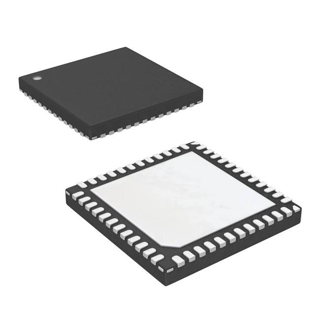
The ISLA224S is available in a space-saving 7mmx7mm 48 Ld
QFN package. The package features a thermal pad for
improved thermal performance and is specified over the full
industrial temperature range (-40°C to +85°C).
• Radar and Satellite Antenna Array Processing
• JESD204A/B High Speed Data Interface
- JESD204A Compliant
- JESD204B Device Subclass 0 Compliant
- JESD204B Device Subclass 2 Compatible
- Up to 3 JESD204 Output Lanes Running up to 4.375Gbps
- Highly Configurable JESD204 Transmitter
• Multiple Chip Time Alignment and Deterministic Latency
Support (JESD204B Device Subclass 2)
• 48-pin QFN 7mmx7mm Package
Key Specifications
• SNR @ 250/200/125MSPS
73.2/74.1/75.1 dBFS fIN = 30MHz
72.4/72.9/73.2 dBFS fIN = 190MHz
82/91/94 dBc fIN = 30MHz
84/82/81 dBc fIN = 190MHz
• Total Power Consumption: 989mW @ 250MSPS
Applications
• Broadband Communications and Microwave Receivers
• High-Performance Data Acquisition
• Communications Test Equipment
• High-Speed Medical Imaging
Pin-Compatible Family
RESOLUTION
SPEED
(MSPS)
PRODUCT
AVAILABILITY
ISLA224S25
14
250
Now
ISLA224S20
14
200
Now
ISLA224S12
14
125
Now
ISLA222S25
12
250
Now
ISLA222S20
12
200
Now
ISLA222S12
12
125
Now
MODEL
FIGURE 1. SERDES DATA EYE AT 4.375Gbps
FN7911 Rev 2.00
April 25, 2013
Page 1 of 38
�CLKP
OVDD
OVDD
(PLL)
SYNC
AVDD
ISLA224S
CLOCK
GENERATION
CLKN
AINP
14-BIT
250MSPS
ADC
SHA
AINN
LANE[2:0]P
LANE[2:0]N
VREF
JESD204
TRANSMITTER
VCM
BINP
14-BIT
250MSPS
ADC
SHA
BINN
VREF
+
–
OVSS
CSB
SCLK
SDIO
SDO
SPI
CONTROL
RESETN
AVSS
(PLL)
NAPSLP
AVSS
1.25V
FIGURE 2. BLOCK DIAGRAM
Pin Configuration
FN7911 Rev 2.00
April 25, 2013
DNC
DNC
AVDD
NAPSLP
CLKDIV
SDIO
SCLK
CSB
SDO
OVDD
OVSS
OVSS
ISLA224S
(48 LD QFN)
TOP VIEW
48
47
46
45
44
43
42
41
40
39
38
37
VCM
1
36 OVDD
AVDD
2
35 OVSS
AVSS
3
34 LANE2N
BINP
4
33 LANE2P
BINN
5
32 OVSS
AVSS
6
31 LANE1N
AVSS
7
30 LANE1P
AINN
8
29 OVSS
AINP
9
28 LANE0N
AVSS
10
27 LANE0P
AVDD
11
DNC
12
26 OVSS
PAD – Exposed Paddle
13
14
15
16
17
18
19
20
21
22
23
24
RESETN
AVDD
AVDD
CLKP
CLKN
SYNCP
SYNCN
DNC
OVSS (PLL)
OVDD (PLL)
OVSS (PLL)
OVDD (PLL)
25 OVDD
Page 2 of 38
�ISLA224S
Pin Descriptions
PIN NUMBER
NAME
FUNCTION
2, 11, 14, 15, 46
AVDD
1.8V Analog Supply
12, 20, 47, 48
DNC
Do Not Connect
3, 6, 7, 10
AVSS
Analog Ground
4, 5
BINP, BINN
B-Channel Analog Input Positive, Negative
8, 9
AINN, AINP
A-Channel Analog Input Negative, Positive
1
VCM
44
CLKDIV
16, 17
CLKP, CLKN
45
NAPSLP
Power Control (Nap, Sleep modes)
13
RESETN
Power On Reset (Active Low)
26, 29, 32, 35, 37, 38
OVSS
Output Ground
25, 36, 39
OVDD
1.8V Digital Supply
22, 24
OVDD (PLL)
1.8V Analog Supply for SERDES PLL
21, 23
OVSS (PLL)
Analog Ground Supply for SERDES PLL
18, 19
SYNCP, SYNCN
27, 28
LANE0P, LANE0N
SERDES Lane 0
30, 31
LANE1P, LANE1N
SERDES Lane 1
33, 34
LANE2P, LANE2N
SERDES Lane 2
40
SDO
SPI Serial Data Output
41
CSB
SPI Chip Select (active low)
42
SCLK
SPI Clock
43
SDIO
SPI Serial Data Input/Output
PAD
AVSS
Exposed Paddle. Analog Ground (connect to AVSS)
Common Mode Output
Clock Divider Control
Clock Input True, Complement
JESD204 SYNC Input
Ordering Information
PART NUMBER
(Notes 1, 2)
PART
MARKING
TEMP. RANGE
(°C)
PACKAGE
(Pb-free)
PKG.
DWG. #
ISLA224S25IR1Z
ISLA224S25 IR1Z
-40 to +85
48 Ld QFN
L48.7x7G
ISLA224S20IR1Z
ISLA224S20 IR1Z
-40 to +85
48 Ld QFN
L48.7x7G
ISLA224S12IR1Z
ISLA224S12 IR1Z
-40 to +85
48 Ld QFN
L48.7x7G
Coming Soon
ISLA224S25IR48EV1Z
FMC Based Evaluation Board (Supports 125/200/250 speed grades), Interfaces with ADCMB-HSFMC-EV1Z
Motherboard and Other FPGA Vendor FMC Based Evaluation Platforms
Coming Soon
ADCMB-HSFMC-EV1Z
FMC Based Motherboard
NOTES:
1. These Intersil Pb-free plastic packaged products employ special Pb-free material sets; molding compounds/die attach materials and NiPdAu plate-e4
termination finish, which is RoHS compliant and compatible with both SnPb and Pb-free soldering operations. Intersil Pb-free products are MSL
classified at Pb-free peak reflow temperatures that meet or exceed the Pb-free requirements of IPC/JEDEC J STD-020.
2. For Moisture Sensitivity Level (MSL), please see device information page for ISLA224S12, ISLA224S20, ISLA224S25. For more information on MSL
please see techbrief TB363.
FN7911 Rev 2.00
April 25, 2013
Page 3 of 38
�ISLA224S
Table of Contents
Absolute Maximum Ratings . . . . . . . . . . . . . . . . . . . . . . . . . . . . . . . . . . . . . . . . . . . . . . . . . . . . . . . . . . . . . . . . . . . . . . . . . . . . . . . . . . . 5
Thermal Information . . . . . . . . . . . . . . . . . . . . . . . . . . . . . . . . . . . . . . . . . . . . . . . . . . . . . . . . . . . . . . . . . . . . . . . . . . . . . . . . . . . . . . . . . 5
Recommended Operating Conditions . . . . . . . . . . . . . . . . . . . . . . . . . . . . . . . . . . . . . . . . . . . . . . . . . . . . . . . . . . . . . . . . . . . . . . . . . . 5
Electrical Specifications . . . . . . . . . . . . . . . . . . . . . . . . . . . . . . . . . . . . . . . . . . . . . . . . . . . . . . . . . . . . . . . . . . . . . . . . . . . . . . . . . . . . . 5
Digital Specifications . . . . . . . . . . . . . . . . . . . . . . . . . . . . . . . . . . . . . . . . . . . . . . . . . . . . . . . . . . . . . . . . . . . . . . . . . . . . . . . . . . . . . . . . 8
Switching Specifications . . . . . . . . . . . . . . . . . . . . . . . . . . . . . . . . . . . . . . . . . . . . . . . . . . . . . . . . . . . . . . . . . . . . . . . . . . . . . . . . . . . . . 8
Typical Performance Curves . . . . . . . . . . . . . . . . . . . . . . . . . . . . . . . . . . . . . . . . . . . . . . . . . . . . . . . . . . . . . . . . . . . . . . . . . . . . . . . . . 10
Theory of Operation. . . . . . . . . . . . . . . . . . . . . . . . . . . . . . . . . . . . . . . . . . . . . . . . . . . . . . . . . . . . . . . . . . . . . . . . . . . . . . . . . . . . . . . . .
Functional Description . . . . . . . . . . . . . . . . . . . . . . . . . . . . . . . . . . . . . . . . . . . . . . . . . . . . . . . . . . . . . . . . . . . . . . . . . . . . . . . . . . . . . . . . . . .
Power-On Calibration. . . . . . . . . . . . . . . . . . . . . . . . . . . . . . . . . . . . . . . . . . . . . . . . . . . . . . . . . . . . . . . . . . . . . . . . . . . . . . . . . . . . . . . . . . . . .
User Initiated Reset . . . . . . . . . . . . . . . . . . . . . . . . . . . . . . . . . . . . . . . . . . . . . . . . . . . . . . . . . . . . . . . . . . . . . . . . . . . . . . . . . . . . . . . . . . . . . .
15
15
15
16
Temperature Calibration. . . . . . . . . . . . . . . . . . . . . . . . . . . . . . . . . . . . . . . . . . . . . . . . . . . . . . . . . . . . . . . . . . . . . . . . . . . . . . . . . . . . .
Analog Input . . . . . . . . . . . . . . . . . . . . . . . . . . . . . . . . . . . . . . . . . . . . . . . . . . . . . . . . . . . . . . . . . . . . . . . . . . . . . . . . . . . . . . . . . . . . . . . . . . . .
Clock Input . . . . . . . . . . . . . . . . . . . . . . . . . . . . . . . . . . . . . . . . . . . . . . . . . . . . . . . . . . . . . . . . . . . . . . . . . . . . . . . . . . . . . . . . . . . . . . . . . . . . .
Jitter. . . . . . . . . . . . . . . . . . . . . . . . . . . . . . . . . . . . . . . . . . . . . . . . . . . . . . . . . . . . . . . . . . . . . . . . . . . . . . . . . . . . . . . . . . . . . . . . . . . . . . . . . . .
Voltage Reference . . . . . . . . . . . . . . . . . . . . . . . . . . . . . . . . . . . . . . . . . . . . . . . . . . . . . . . . . . . . . . . . . . . . . . . . . . . . . . . . . . . . . . . . . . . . . . .
Digital Outputs . . . . . . . . . . . . . . . . . . . . . . . . . . . . . . . . . . . . . . . . . . . . . . . . . . . . . . . . . . . . . . . . . . . . . . . . . . . . . . . . . . . . . . . . . . . . . . . . . .
Power Dissipation . . . . . . . . . . . . . . . . . . . . . . . . . . . . . . . . . . . . . . . . . . . . . . . . . . . . . . . . . . . . . . . . . . . . . . . . . . . . . . . . . . . . . . . . . . . . . . .
Nap/Sleep. . . . . . . . . . . . . . . . . . . . . . . . . . . . . . . . . . . . . . . . . . . . . . . . . . . . . . . . . . . . . . . . . . . . . . . . . . . . . . . . . . . . . . . . . . . . . . . . . . . . . .
Data Format . . . . . . . . . . . . . . . . . . . . . . . . . . . . . . . . . . . . . . . . . . . . . . . . . . . . . . . . . . . . . . . . . . . . . . . . . . . . . . . . . . . . . . . . . . . . . . . . . . . .
17
18
18
19
19
19
19
19
20
Clock Divider Synchronous Reset . . . . . . . . . . . . . . . . . . . . . . . . . . . . . . . . . . . . . . . . . . . . . . . . . . . . . . . . . . . . . . . . . . . . . . . . . . . . . 20
Soft Reset . . . . . . . . . . . . . . . . . . . . . . . . . . . . . . . . . . . . . . . . . . . . . . . . . . . . . . . . . . . . . . . . . . . . . . . . . . . . . . . . . . . . . . . . . . . . . . . . . 20
JESD204 Transmitter . . . . . . . . . . . . . . . . . . . . . . . . . . . . . . . . . . . . . . . . . . . . . . . . . . . . . . . . . . . . . . . . . . . . . . . . . . . . . . . . . . . . . . . . 20
Overview . . . . . . . . . . . . . . . . . . . . . . . . . . . . . . . . . . . . . . . . . . . . . . . . . . . . . . . . . . . . . . . . . . . . . . . . . . . . . . . . . . . . . . . . . . . . . . . . . . . . . . . 20
Initial Lane Alignment . . . . . . . . . . . . . . . . . . . . . . . . . . . . . . . . . . . . . . . . . . . . . . . . . . . . . . . . . . . . . . . . . . . . . . . . . . . . . . . . . . . . . . . . . . . . 21
Test Patterns . . . . . . . . . . . . . . . . . . . . . . . . . . . . . . . . . . . . . . . . . . . . . . . . . . . . . . . . . . . . . . . . . . . . . . . . . . . . . . . . . . . . . . . . . . . . . . 22
Serial Peripheral Interface . . . . . . . . . . . . . . . . . . . . . . . . . . . . . . . . . . . . . . . . . . . . . . . . . . . . . . . . . . . . . . . . . . . . . . . . . . . . . . . . . .
SPI Physical Interface . . . . . . . . . . . . . . . . . . . . . . . . . . . . . . . . . . . . . . . . . . . . . . . . . . . . . . . . . . . . . . . . . . . . . . . . . . . . . . . . . . . . . . . . . . . .
SPI Configuration. . . . . . . . . . . . . . . . . . . . . . . . . . . . . . . . . . . . . . . . . . . . . . . . . . . . . . . . . . . . . . . . . . . . . . . . . . . . . . . . . . . . . . . . . . . . . . . .
Device Information . . . . . . . . . . . . . . . . . . . . . . . . . . . . . . . . . . . . . . . . . . . . . . . . . . . . . . . . . . . . . . . . . . . . . . . . . . . . . . . . . . . . . . . . . . . . . .
Device Configuration/Control. . . . . . . . . . . . . . . . . . . . . . . . . . . . . . . . . . . . . . . . . . . . . . . . . . . . . . . . . . . . . . . . . . . . . . . . . . . . . . . . . . . . . .
Global Device Configuration/Control . . . . . . . . . . . . . . . . . . . . . . . . . . . . . . . . . . . . . . . . . . . . . . . . . . . . . . . . . . . . . . . . . . . . . . . . . . . . . . .
ADDRESS 0xDF - 0xF3: JESD204 REGISTERS . . . . . . . . . . . . . . . . . . . . . . . . . . . . . . . . . . . . . . . . . . . . . . . . . . . . . . . . . . . . . . . . . . . . . . . .
Address 0xDF-0xEE: JESD204 Parameter INTERFACE . . . . . . . . . . . . . . . . . . . . . . . . . . . . . . . . . . . . . . . . . . . . . . . . . . . . . . . . . . . . . . . . .
25
25
26
26
26
27
29
29
SPI Memory Map . . . . . . . . . . . . . . . . . . . . . . . . . . . . . . . . . . . . . . . . . . . . . . . . . . . . . . . . . . . . . . . . . . . . . . . . . . . . . . . . . . . . . . . . . . . 31
Equivalent Circuits . . . . . . . . . . . . . . . . . . . . . . . . . . . . . . . . . . . . . . . . . . . . . . . . . . . . . . . . . . . . . . . . . . . . . . . . . . . . . . . . . . . . . . . . . 35
ADC Evaluation Platform . . . . . . . . . . . . . . . . . . . . . . . . . . . . . . . . . . . . . . . . . . . . . . . . . . . . . . . . . . . . . . . . . . . . . . . . . . . . . . . . . . . . 36
Layout Considerations . . . . . . . . . . . . . . . . . . . . . . . . . . . . . . . . . . . . . . . . . . . . . . . . . . . . . . . . . . . . . . . . . . . . . . . . . . . . . . . . . . . . . .
Split Ground and Power Planes . . . . . . . . . . . . . . . . . . . . . . . . . . . . . . . . . . . . . . . . . . . . . . . . . . . . . . . . . . . . . . . . . . . . . . . . . . . . . . . . . . . .
Clock Input Considerations. . . . . . . . . . . . . . . . . . . . . . . . . . . . . . . . . . . . . . . . . . . . . . . . . . . . . . . . . . . . . . . . . . . . . . . . . . . . . . . . . . . . . . . .
Exposed Paddle . . . . . . . . . . . . . . . . . . . . . . . . . . . . . . . . . . . . . . . . . . . . . . . . . . . . . . . . . . . . . . . . . . . . . . . . . . . . . . . . . . . . . . . . . . . . . . . . .
Bypass and Filtering . . . . . . . . . . . . . . . . . . . . . . . . . . . . . . . . . . . . . . . . . . . . . . . . . . . . . . . . . . . . . . . . . . . . . . . . . . . . . . . . . . . . . . . . . . . . .
CML Outputs . . . . . . . . . . . . . . . . . . . . . . . . . . . . . . . . . . . . . . . . . . . . . . . . . . . . . . . . . . . . . . . . . . . . . . . . . . . . . . . . . . . . . . . . . . . . . . . . . . . .
Unused Inputs . . . . . . . . . . . . . . . . . . . . . . . . . . . . . . . . . . . . . . . . . . . . . . . . . . . . . . . . . . . . . . . . . . . . . . . . . . . . . . . . . . . . . . . . . . . . . . . . . .
36
36
36
36
36
36
36
Definitions . . . . . . . . . . . . . . . . . . . . . . . . . . . . . . . . . . . . . . . . . . . . . . . . . . . . . . . . . . . . . . . . . . . . . . . . . . . . . . . . . . . . . . . . . . . . . . . . 36
Revision History. . . . . . . . . . . . . . . . . . . . . . . . . . . . . . . . . . . . . . . . . . . . . . . . . . . . . . . . . . . . . . . . . . . . . . . . . . . . . . . . . . . . . . . . . . . . 37
About Intersil . . . . . . . . . . . . . . . . . . . . . . . . . . . . . . . . . . . . . . . . . . . . . . . . . . . . . . . . . . . . . . . . . . . . . . . . . . . . . . . . . . . . . . . . . . . . . . 37
Package Outline Drawing . . . . . . . . . . . . . . . . . . . . . . . . . . . . . . . . . . . . . . . . . . . . . . . . . . . . . . . . . . . . . . . . . . . . . . . . . . . . . . . . . . . . 38
FN7911 Rev 2.00
April 25, 2013
Page 4 of 38
�ISLA224S
Absolute Maximum Ratings
Thermal Information
AVDD to AVSS . . . . . . . . . . . . . . . . . . . . . . . . . . . . . . . . . . . . . . . .-0.4V to 2.1V
OVDD to OVSS . . . . . . . . . . . . . . . . . . . . . . . . . . . . . . . . . . . . . . . .-0.4V to 2.1V
AVSS to OVSS . . . . . . . . . . . . . . . . . . . . . . . . . . . . . . . . . . . . . . . -0.3V to 0.3V
Analog Inputs to AVSS . . . . . . . . . . . . . . . . . . . . . . . . . -0.4V to AVDD + 0.3V
Clock Inputs to AVSS . . . . . . . . . . . . . . . . . . . . . . . . . . -0.4V to AVDD + 0.3V
Logic Input to AVSS . . . . . . . . . . . . . . . . . . . . . . . . . . . -0.4V to OVDD + 0.3V
Logic Inputs to OVSS . . . . . . . . . . . . . . . . . . . . . . . . . . -0.4V to OVDD + 0.3V
Latchup (Tested per JESD-78C;Class 2,Level A) . . . . . . . . . . . . . . . . 100mA
Thermal Resistance (Typical)
JA (°C/W) JC (°C/W)
48 Ld QFN (Notes 3, 4, 5) . . . . . . . . . . . . . .
24
0.4
Storage Temperature . . . . . . . . . . . . . . . . . . . . . . . . . . . . . .-65°C to +150°C
Junction Temperature . . . . . . . . . . . . . . . . . . . . . . . . . . . . . . . . . . . . .+150°C
Pb-Free Reflow Profile . . . . . . . . . . . . . . . . . . . . . . . . . . . . . . . see link below
http://www.intersil.com/pbfree/Pb-FreeReflow.asp
Recommended Operating Conditions
Operating Temperature . . . . . . . . . . . . . . . . . . . . . . . . . . . . . -40°C to +85°C
NOTES:
3. JA is measured in free air with the component mounted on a high effective thermal conductivity test board with “direct attach” features. See Tech
Brief TB379.
4. For JC, the “case temp” location is the center of the exposed metal pad on the package underside.
5. For solder stencil layout and reflow guidelines, please see Tech Brief TB389.
CAUTION: Do not operate at or near the maximum ratings listed for extended periods of time. Exposure to such conditions may adversely impact product
reliability and result in failures not covered by warranty.
Electrical Specifications All specifications apply under the following conditions unless otherwise noted: AVDD = 1.8V, OVDD = 1.8V,
TA = -40°C to +85°C (typical specifications at +25°C), AIN = -2dBFS, fSAMPLE = Maximum Conversion Rate (per speed grade). Boldface limits apply
over the operating temperature range, -40°C to +85°C.
ISLA224S25
PARAMETER
SYMBOL
CONDITIONS
MIN
(Note 6)
TYP
1.95
2.00
ISLA224S20
ISLA224S12
MAX
MIN
MAX
MIN
MAX
(Note 6) (Note 6) TYP (Note 6) (Note 6) TYP (Note 6)
UNITS
DC SPECIFICATIONS
Analog Input
Full-Scale Analog Input
Range
VFS
Differential
2.15
1.95
2.0
2.15
1.9
2.0
2.1
VP-P
Input Resistance
RIN
Differential
600
600
600
Input Capacitance
CIN
Differential
7.4
7.4
7.4
pF
Full Temp
115
58
58
ppm/°C
Full Scale Range Temp.
Drift
AVTC
Input Offset Voltage
VOS
Gain Error
EG
1
1
1
%
Common-Mode Output
Voltage
VCM
0.94
0.94
0.94
V
Common Mode Input
Current (per pin)
ICM
6.0
6.0
6.0
µA/MSPS
Inputs Common Mode
Voltage
0.9
0.9
0.9
V
CLKP, CLKN Swing
1.8
1.8
1.8
V
-5.0
±1
5.0
-5.0
±1
5.0
-5.0
±1
5.0
mV
Clock Inputs
Power Requirements
1.8V Analog Supply
Voltage
AVDD
1.7
1.8
1.9
1.7
1.8
1.9
1.7
1.8
1.9
V
1.8V Digital Supply
Voltage
OVDD
1.7
1.8
1.9
1.7
1.8
1.9
1.7
1.8
1.9
V
1.8V Analog Supply
Current
IAVDD
353
375
324
344
282
316
mA
1.8V Digital Supply
Current
IOVDD
195
213
179
196
123
173
mA
FN7911 Rev 2.00
April 25, 2013
Minimum number of
lanes active
Page 5 of 38
�ISLA224S
Electrical Specifications All specifications apply under the following conditions unless otherwise noted: AVDD = 1.8V, OVDD = 1.8V,
TA = -40°C to +85°C (typical specifications at +25°C), AIN = -2dBFS, fSAMPLE = Maximum Conversion Rate (per speed grade). Boldface limits apply
over the operating temperature range, -40°C to +85°C. (Continued)
ISLA224S25
PARAMETER
SYMBOL
Power Supply Rejection
Ratio (Note 7)
PSRR
CONDITIONS
MIN
(Note 6)
TYP
ISLA224S20
ISLA224S12
MAX
MIN
MAX
MIN
MAX
(Note 6) (Note 6) TYP (Note 6) (Note 6) TYP (Note 6)
UNITS
30MHz 200mVp-p
40
40
40
dB
1MHz 200mVp-p
47
47
47
dB
Total Power Dissipation
Normal Mode
PD
989
1058
910
972
731
843
mW
Nap Mode
PD
447
490
391
453
290
398
mW
Sleep Mode
PD
CSB at logic high
5
12
5
12
6
12
mW
Nap Mode Wakeup
Time
Sample Clock
Running
5
5
5
µs
Sleep Mode Wakeup
Time
Sample Clock
Running
1
1
1
ms
±0.18
LSB
±2.0
LSB
50
MSPS
AC SPECIFICATIONS (Note 8)
Differential Nonlinearity
DNL
Integral Nonlinearity
INL
Minimum Conversion
Rate (Note 9)
fS MIN
fIN=105MHz
No Missing Codes
-1.0
±0.4
1.5
-0.5
±3.0
±0.2
-1.0
±2.0
100
ISLA224S25/20
(3 Lanes, Efficient
Packing)
1
100
ISLA224S12 (2 Lanes,
Simple Packing)
Maximum Conversion
Rate (Note 9)
fS MAX
Efficient Packing
250
200
Simple Packing
125
155
MSPS
125
MSPS
Minimum Serdes Lane
Data Rate
Independent of Packing
Mode
1.0
1.0
1.0
GBPS
Maximum Serdes Lane
Data Rate
Independent of Packing
Mode
4.375
4.375
4.375
GBPS
fIN = 30MHz
73.1
73.8
75.1
dBFS
74.4
dBFS
(See “Lane data rate” on
page 22.)
Signal-to-Noise Ratio
(Note 10)
Signal-to-Noise and
Distortion (Note 10)
FN7911 Rev 2.00
April 25, 2013
SNR
fIN = 105MHz
SINAD
70.8
72.9
72.5
73.6
73.0
fIN = 190MHz
72.4
72.9
73.2
dBFS
fIN = 363MHz
71.1
71.1
70.6
dBFS
fIN = 495MHz
70.0
69.5
68.8
dBFS
fIN = 605MHz
69.0
68.3
67.3
dBFS
fIN = 30MHz
72.9
73.7
74.8
dBFS
74.1
dBFS
fIN = 105MHz
68.8
72.5
72.0
73.4
72.7
fIN = 190MHz
72.1
72.1
72.4
dBFS
fIN = 363MHz
70.1
70.3
67.5
dBFS
fIN = 495MHz
66.5
65.8
62.8
dBFS
fIN = 605MHz
58.8
58.5
54.7
dBFS
Page 6 of 38
�ISLA224S
Electrical Specifications All specifications apply under the following conditions unless otherwise noted: AVDD = 1.8V, OVDD = 1.8V,
TA = -40°C to +85°C (typical specifications at +25°C), AIN = -2dBFS, fSAMPLE = Maximum Conversion Rate (per speed grade). Boldface limits apply
over the operating temperature range, -40°C to +85°C. (Continued)
ISLA224S25
PARAMETER
SYMBOL
Effective Number of Bits
(Note 10)
ENOB
Spurious-Free Dynamic
Range (Note 10)
Spurious-Free Dynamic
Range Excluding H2, H3
(Note 10)
Intermodulation
Distortion
CONDITIONS
fIN = 30MHz
fIN = 105MHz
SFDR
MIN
(Note 6)
11.8
11.9
11.67
11.9
11.78
UNITS
12.1
Bits
12.0
Bits
11.7
11.7
11.7
Bits
fIN = 363MHz
11.4
11.4
10.9
Bits
fIN = 495MHz
10.8
10.6
10.1
Bits
fIN = 605MHz
9.5
9.4
8.8
Bits
fIN = 30MHz
86
89
94
dBc
86
dBc
74
85
76
88
76
fIN = 190MHz
84
82
81
dBc
fIN = 363MHz
78
79
69
dBc
fIN = 495MHz
68
67
62
dBc
fIN = 605MHz
58
57
53
dBc
87
90
96
dBc
fIN = 105MHz
89
92
94
dBc
fIN = 190MHz
89
91
92
dBc
fIN = 363MHz
86
88
87
dBc
fIN = 495MHz
86
84
84
dBc
fIN = 605MHz
85
83
82
dBc
fIN = 70MHz
83
83
83
dBFS
fIN = 170MHz
97
95
95
dBFS
fIN = 10MHz
88
90
100
dB
fIN = 124MHz
82
87
86
dB
10-13
10-13
675
675
SFDRX23 fIN = 30MHz
Channel-to-Channel
Isolation
MAX
MIN
MAX
MIN
MAX
(Note 6) (Note 6) TYP (Note 6) (Note 6) TYP (Note 6)
11.8
11.14
ISLA224S12
fIN = 190MHz
fIN = 105MHz
IMD
TYP
ISLA224S20
Word Error Rate
WER
10-13
Full Power Bandwidth
FPBW
675
MHz
NOTES:
6. Compliance to datasheet limits is assured by one or more methods: production test, characterization and/or design.
7. PSRR is calculated by the equation 20*log10(A/B), where B is the amplitude of a disturber sinusoid on AVDD at the device pins, and A is the amplitude
of the spur in the captured data at the frequency of the disturber sinusoid.
8. AC Specifications apply after internal calibration of the ADC is invoked at the given sample rate and temperature. Refer to “Power-On Calibration” on
page 15 and “User Initiated Reset” on page 16 for more detail.
9. The DLL Range setting must be changed via SPI for ADC core sample rates below 80MSPS. The JESD204 transmitter can support ADC sample rates
below 100MSPS, as long as the SERDES lane data rate is greater than or equal to 1Gbps.
10. Minimum specification guaranteed when calibrated at +85°C.
FN7911 Rev 2.00
April 25, 2013
Page 7 of 38
�ISLA224S
Digital Specifications
Boldface limits apply over the operating temperature range, -40°C to +85°C.
PARAMETER
SYMBOL
CONDITIONS
MIN
(Note 6)
TYP
MAX
(Note 6) UNITS
CMOS INPUTS
Input Current High (RESETN)
IIH
VIN = 1.8V
1
10
µA
Input Current Low (RESETN)
IIL
VIN = 0V
-12
-7
µA
Input Current High (SDIO, SCL, SDA SCLK)
IIH
VIN = 1.8V
4
12
µA
Input Current Low (SDIO, SCL, SDA SCLK)
IIL
VIN = 0V
-600
-400
-300
µA
Input Current High (CSB)
IIH
VIN = 1.8V
40
52
70
µA
Input Current Low (CSB)
IIL
VIN = 0V
1
10
µA
Input Voltage High (SDIO, RESETN)
VIH
Input Voltage Low (SDIO, RESETN)
VIL
Input Current High (NAPSLP, CLKDIV) (Note 11)
IIH
19
Input Current Low (NAPSLP, CLKDIV)
IIL
--30
Input Capacitance
CDI
-25
1.17
V
0.63
V
25
30
µA
-25
-19
µA
4
pF
LVDS INPUTS (SYNCP, SYNCN)
Input Common Mode Range
VICM
825
1575
mV
Input Differential Swing (peak-to-peak, single-ended)
VID
250
450
mV
Input Pull-up and Pull-down Resistance
RIpu
100
kΩ
1.14
V
CML OUTPUTS
Output Common Mode Voltage
Switching Specifications
Boldface limits apply over the operating temperature range, -40°C to +85°C.
PARAMETER
SYMBOL
CONDITION
MIN
(Note 6)
TYP
MAX
(Note 6)
UNITS
ADC OUTPUT
Aperture Delay
tA
190
ps
RMS Aperture Jitter
jA
100
fs
250
µs
L
10
cycles
tOVR
1
cycles
PLL Lock Time
250
µs
PLL Bandwidth
2.2
MHz
Added Random Jitter
5
ps
RMS
Added Deterministic Jitter
7
ps P-P
5
ps rms
Synchronous Clock Divider Reset Recovery Time (Note 12)
Latency (ADC Pipeline Delay)
Overvoltage Recovery
tRSTRT
DLL recovery
time after
Synchronous
Reset
SERDES
Maximum Input Sample Clock Total Jitter to Maintain SERDES
BER