Datasheet
KAD5514P
14-Bit, 250/210/170/125MSPS ADC
The KAD5514P (KAD5514P-12, KAD5514P-17,
KAD5514P-21, KAD5514P-25) is a family of
low-power, high performance 14-bit, analog-to-digital
converters. The family is designed with the proprietary
FemtoCharge™ technology on a standard CMOS
process, and supports sampling rates of up to
250MSPS. The KAD5514P is part of a pin-compatible
portfolio of 10, 12, and 14-bit ADCs with sample rates
ranging from 125MSPS to 500MSPS.
Features
A Serial Peripheral Interface (SPI) port allows for
extensive configurability and fine control of various
parameters such as gain and offset.
• Nap and sleep modes
Digital output data is presented in selectable LVDS or
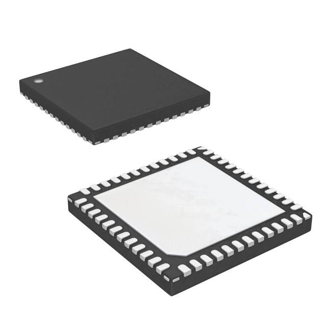
CMOS formats. The KAD5514P is available in 72 Ld
and 48 Ld QFN packages with an exposed paddle.
The devices operate from a 1.8V supply, and
performance is specified across the full industrial
temperature range (-40°C to +85°C).
• DDR LVDS-compatible or LVCMOS outputs
• Programmable gain, offset, and skew control
• 950MHz analog input bandwidth
• 60fs clock jitter
• Over-range indicator
• Selectable clock divider: ÷1, ÷2, or ÷4
• Clock phase selection
• Two’s complement, gray code or binary data format
• Programmable built-in test patterns
• Single-supply 1.8V operation
• Pb-free (RoHS compliant)
Key Specifications
Applications
• SNR = 69.4dBFS for fIN = 105MHz (-1dBFS)
• Power amplifier linearization
• SFDR = 82.2dBc for fIN = 105MHz (-1dBFS)
• Radar and satellite antenna array processing
• Total power consumption
• Broadband communications
○ 429/345mW at 250/125MSPS (SDR Mode)
• High-performance data acquisition
○ 390/309mW at 250/125MSPS (DDR Mode)
• Communications test equipment
Related Literature
• WiMAX and microwave receivers
For a full list of related documents, visit our website:
CLKP
OVDD
AVDD
CLKDIV
• KAD5514P-12, KAD5514P-17, KAD5514P-21,
KAD5514P-25 device pages
CLKOUTP
Clock
Generation
VINP
14-Bit
250 MSPS
ADC
VCM
AVSS
NAPSLP
1.25V
+
–
SPI
Control
D[13:0]P
D[13:0]N
Digital
Error
Correction
ORP
ORN
LVDS/CMOS
Drivers
CSB
SCLK
SDIO
SDO
SHA
VINN
CLKOUTN
OUTFMT
OUTMODE
OVSS
CLKN
Figure 1. Block Diagram
FN6804 Rev.4.00
Jun.17.19
Page 1 of 44
�KAD5514P
Contents
1.
Overview . . . . . . . . . . . . . . . . . . . . . . . . . . . . . . . . . . . . . . . . . . . . . . . . . . . . . . . . . . . . . . . . . . . . . . . . . . . 4
1.1
1.2
1.3
2.
Ordering Information . . . . . . . . . . . . . . . . . . . . . . . . . . . . . . . . . . . . . . . . . . . . . . . . . . . . . . . . . . . . . . . 4
Pin Configurations . . . . . . . . . . . . . . . . . . . . . . . . . . . . . . . . . . . . . . . . . . . . . . . . . . . . . . . . . . . . . . . . . 5
Pin Descriptions . . . . . . . . . . . . . . . . . . . . . . . . . . . . . . . . . . . . . . . . . . . . . . . . . . . . . . . . . . . . . . . . . . . 6
Specifications. . . . . . . . . . . . . . . . . . . . . . . . . . . . . . . . . . . . . . . . . . . . . . . . . . . . . . . . . . . . . . . . . . . . . . 10
2.1
2.2
2.3
2.4
2.5
2.6
Absolute Maximum Ratings . . . . . . . . . . . . . . . . . . . . . . . . . . . . . . . . . . . . . . . . . . . . . . . . . . . . . . . . .
Thermal Information. . . . . . . . . . . . . . . . . . . . . . . . . . . . . . . . . . . . . . . . . . . . . . . . . . . . . . . . . . . . . . .
Electrical Specifications . . . . . . . . . . . . . . . . . . . . . . . . . . . . . . . . . . . . . . . . . . . . . . . . . . . . . . . . . . . .
Digital Specifications . . . . . . . . . . . . . . . . . . . . . . . . . . . . . . . . . . . . . . . . . . . . . . . . . . . . . . . . . . . . . .
Timing Diagrams . . . . . . . . . . . . . . . . . . . . . . . . . . . . . . . . . . . . . . . . . . . . . . . . . . . . . . . . . . . . . . . . .
Switching Specifications . . . . . . . . . . . . . . . . . . . . . . . . . . . . . . . . . . . . . . . . . . . . . . . . . . . . . . . . . . .
10
10
11
13
14
14
3.
Typical Performance Curves. . . . . . . . . . . . . . . . . . . . . . . . . . . . . . . . . . . . . . . . . . . . . . . . . . . . . . . . . . 16
4.
Theory of Operation. . . . . . . . . . . . . . . . . . . . . . . . . . . . . . . . . . . . . . . . . . . . . . . . . . . . . . . . . . . . . . . . . 19
4.1
4.2
4.3
4.4
4.5
4.6
4.7
4.8
4.9
4.10
4.11
4.12
5.
Functional Description . . . . . . . . . . . . . . . . . . . . . . . . . . . . . . . . . . . . . . . . . . . . . . . . . . . . . . . . . . . . .
Power-On Calibration . . . . . . . . . . . . . . . . . . . . . . . . . . . . . . . . . . . . . . . . . . . . . . . . . . . . . . . . . . . . .
User-Initiated Reset . . . . . . . . . . . . . . . . . . . . . . . . . . . . . . . . . . . . . . . . . . . . . . . . . . . . . . . . . . . . . . .
Analog Input. . . . . . . . . . . . . . . . . . . . . . . . . . . . . . . . . . . . . . . . . . . . . . . . . . . . . . . . . . . . . . . . . . . . .
Clock Input. . . . . . . . . . . . . . . . . . . . . . . . . . . . . . . . . . . . . . . . . . . . . . . . . . . . . . . . . . . . . . . . . . . . . .
Jitter . . . . . . . . . . . . . . . . . . . . . . . . . . . . . . . . . . . . . . . . . . . . . . . . . . . . . . . . . . . . . . . . . . . . . . . . . . .
Voltage Reference . . . . . . . . . . . . . . . . . . . . . . . . . . . . . . . . . . . . . . . . . . . . . . . . . . . . . . . . . . . . . . . .
Digital Outputs . . . . . . . . . . . . . . . . . . . . . . . . . . . . . . . . . . . . . . . . . . . . . . . . . . . . . . . . . . . . . . . . . . .
Over-Range Indicator . . . . . . . . . . . . . . . . . . . . . . . . . . . . . . . . . . . . . . . . . . . . . . . . . . . . . . . . . . . . .
Power Dissipation . . . . . . . . . . . . . . . . . . . . . . . . . . . . . . . . . . . . . . . . . . . . . . . . . . . . . . . . . . . . . . . .
Nap/Sleep . . . . . . . . . . . . . . . . . . . . . . . . . . . . . . . . . . . . . . . . . . . . . . . . . . . . . . . . . . . . . . . . . . . . . .
Data Format . . . . . . . . . . . . . . . . . . . . . . . . . . . . . . . . . . . . . . . . . . . . . . . . . . . . . . . . . . . . . . . . . . . . .
19
19
20
21
22
23
23
23
24
24
24
25
Serial Peripheral Interface. . . . . . . . . . . . . . . . . . . . . . . . . . . . . . . . . . . . . . . . . . . . . . . . . . . . . . . . . . . . 27
5.1
5.2
5.3
5.4
5.5
5.6
5.7
SPI Physical Interface . . . . . . . . . . . . . . . . . . . . . . . . . . . . . . . . . . . . . . . . . . . . . . . . . . . . . . . . . . . . .
SPI Configuration. . . . . . . . . . . . . . . . . . . . . . . . . . . . . . . . . . . . . . . . . . . . . . . . . . . . . . . . . . . . . . . . .
Device Information . . . . . . . . . . . . . . . . . . . . . . . . . . . . . . . . . . . . . . . . . . . . . . . . . . . . . . . . . . . . . . . .
Indexed Device Configuration/Control . . . . . . . . . . . . . . . . . . . . . . . . . . . . . . . . . . . . . . . . . . . . . . . . .
Global Device Configuration/Control . . . . . . . . . . . . . . . . . . . . . . . . . . . . . . . . . . . . . . . . . . . . . . . . . .
Device Test . . . . . . . . . . . . . . . . . . . . . . . . . . . . . . . . . . . . . . . . . . . . . . . . . . . . . . . . . . . . . . . . . . . . .
SPI Memory Map . . . . . . . . . . . . . . . . . . . . . . . . . . . . . . . . . . . . . . . . . . . . . . . . . . . . . . . . . . . . . . . . .
27
29
29
30
31
33
34
6.
Equivalent Circuits . . . . . . . . . . . . . . . . . . . . . . . . . . . . . . . . . . . . . . . . . . . . . . . . . . . . . . . . . . . . . . . . . 36
7.
Layout Considerations . . . . . . . . . . . . . . . . . . . . . . . . . . . . . . . . . . . . . . . . . . . . . . . . . . . . . . . . . . . . . . 38
7.1
7.2
7.3
7.4
7.5
7.6
7.7
7.8
Split Ground and Power Planes. . . . . . . . . . . . . . . . . . . . . . . . . . . . . . . . . . . . . . . . . . . . . . . . . . . . . .
Clock Input Considerations . . . . . . . . . . . . . . . . . . . . . . . . . . . . . . . . . . . . . . . . . . . . . . . . . . . . . . . . .
Exposed Paddle. . . . . . . . . . . . . . . . . . . . . . . . . . . . . . . . . . . . . . . . . . . . . . . . . . . . . . . . . . . . . . . . . .
Bypass and Filtering . . . . . . . . . . . . . . . . . . . . . . . . . . . . . . . . . . . . . . . . . . . . . . . . . . . . . . . . . . . . . .
LVDS Outputs . . . . . . . . . . . . . . . . . . . . . . . . . . . . . . . . . . . . . . . . . . . . . . . . . . . . . . . . . . . . . . . . . . .
LVCMOS Outputs . . . . . . . . . . . . . . . . . . . . . . . . . . . . . . . . . . . . . . . . . . . . . . . . . . . . . . . . . . . . . . . .
Unused Inputs . . . . . . . . . . . . . . . . . . . . . . . . . . . . . . . . . . . . . . . . . . . . . . . . . . . . . . . . . . . . . . . . . . .
72 Ld/48 Ld Package Options . . . . . . . . . . . . . . . . . . . . . . . . . . . . . . . . . . . . . . . . . . . . . . . . . . . . . . .
FN6804 Rev.4.00
Jun.17.19
38
38
38
38
38
38
38
38
Page 2 of 44
�KAD5514P
8.
ADC Evaluation Platform . . . . . . . . . . . . . . . . . . . . . . . . . . . . . . . . . . . . . . . . . . . . . . . . . . . . . . . . . . . . 39
9.
Definitions . . . . . . . . . . . . . . . . . . . . . . . . . . . . . . . . . . . . . . . . . . . . . . . . . . . . . . . . . . . . . . . . . . . . . . . . 40
10.
Revision History. . . . . . . . . . . . . . . . . . . . . . . . . . . . . . . . . . . . . . . . . . . . . . . . . . . . . . . . . . . . . . . . . . . . 41
11.
Package Outline Drawings . . . . . . . . . . . . . . . . . . . . . . . . . . . . . . . . . . . . . . . . . . . . . . . . . . . . . . . . . . . 42
FN6804 Rev.4.00
Jun.17.19
Page 3 of 44
�KAD5514P
1.
1.1
1. Overview
Overview
Ordering Information
Part Number
(Note 3)
Part
Marking
Speed
(MSPS)
Temp. Range
(°C)
Package
(RoHS Compliant)
Pkg.
Dwg. #
KAD5514P-25Q72 (Note 1)
KAD5514P-25 Q72EP-I
250
-40 to +85
72 Ld QFN
L72.10X10D
KAD5514P-21Q72 (Note 1)
KAD5514P-21 Q72EP-I
210
-40 to +85
72 Ld QFN
L72.10X10D
KAD5514P-17Q72 (Note 1)
KAD5514P-17 Q72EP-I
170
-40 to +85
72 Ld QFN
L72.10X10D
KAD5514P-12Q72 (Note 1)
KAD5512P-12 Q72EP-I
125
-40 to +85
72 Ld QFN
L72.10X10D
KAD5514P-25Q48 (Note 2)
KAD5512P-25 Q48EP-I
250
-40 to +85
48 Ld QFN
L48.7X7E
KAD5514P-21Q48 (Note 2)
KAD5514P-21 Q48EP-I
210
-40 to +85
48 Ld QFN
L48.7X7E
KAD5514P-17Q48 (Note 2)
KAD5514P-17 Q48EP-I
170
-40 to +85
48 Ld QFN
L48.7X7E
KAD5514P-12Q48 (Note 2)
KAD5514P-12 Q48EP-I
125
-40 to +85
48 Ld QFN
L48.7X7E
Notes:
1. These Pb-free plastic packaged products employ special Pb-free material sets; molding compounds/die attach materials and NiPdAu
plate-e4 termination finish, which is RoHS compliant and compatible with both SnPb and Pb-free soldering operations. Pb-free products
are MSL classified at Pb-free peak reflow temperatures that meet or exceed the Pb-free requirements of IPC/JEDEC J STD-020.
2. These Pb-free plastic packaged products employ special Pb-free material sets, molding compounds/die attach materials, and 100% matte
tin plate plus anneal (e3 termination finish, which is RoHS compliant and compatible with both SnPb and Pb-free soldering operations).
Pb-free products are MSL classified at Pb-free peak reflow temperatures that meet or exceed the Pb-free requirements of IPC/JEDEC J
STD-020.
3. For Moisture Sensitivity Level (MSL), see the KAD5514P-12, KAD5514P-17, KAD5514P-21, KAD5514P-25 device pages. For more
information about MSL, see TB363.
Table 1.
Pin-Compatible Family
Model
Resolution (Bits)
Speed (MSPS)
KAD5514P-25
14
250
KAD5514P-21
14
210
KAD5514P-17
14
170
KAD5514P-12
14
125
KAD5512P-50
12
500
KAD5512P-25, KAD5514P-25
12
250
KAD5512P-21, KAD5514P-21
12
210
KAD5512P-17, KAD5514P-17
12
170
KAD5512P-12, KAD5514P-12
12
125
KAD5510P-50
10
500
FN6804 Rev.4.00
Jun.17.19
Page 4 of 44
�KAD5514P
1.2
1.2.1
1. Overview
Pin Configurations
72 Ld QFN
AVSS
AVDD
OUTFMT
SDIO
SCLK
CSB
SDO
OVSS
ORP
ORN
D13P
D13N
D12P
D12N
D11P
D11N
OVDD
OVSS
72 Ld QFN
Top View
72
71
70
69
68
67
66
65
64
63
62
61
60
59
58
57
56
55
AVDD
1
54 D10P
DNC
2
53 D10N
DNC
3
52 D9P
DNC
4
51 D9N
DNC
5
50 D8P
AVDD
6
49 D8N
AVSS
7
48 CLKOUTP
AVSS
8
47 CLKOUTN
Exposed Paddle
VINN
9
VINP
10
45 OVSS
AVSS
11
44 D7P
AVDD
12
43 D7N
DNC
13
42 D6P
DNC
14
41 D6N
VCM
15
40 D5P
CLKDIV
16
39 D5N
DNC
17
DNC
18
FN6804 Rev.4.00
Jun.17.19
46 RLVDS
38 D4P
Connect Thermal Pad to AVSS
19
20
21
22
23
24
25
26
27
28
29
30
31
32
33
34
35
36
AVDD
CLKP
CLKN
OUTMODE
NAPSLP
AVDD
RESETN
OVSS
OVDD
D0N
D0P
D1N
D1P
D2N
D2P
D3N
D3P
OVDD
37 D4N
Page 5 of 44
�KAD5514P
1.2.2
1. Overview
48 Ld QFN
1.3
AVSS
AVDD
SDIO
SCLK
CSB
SDO
OVSS
ORP
ORN
D6P
D6N
OVDD
48 Ld QFN
Top View
48
47
46
45
44
43
42
41
40
39
38
37
AVDD
1
36 D5P
DNC
2
35 D5N
DNC
3
34 D4P
DNC
4
33 D4N
AVSS
5
32 CLKOUTP
VINN
6
VINP
7
30 RLVDS
AVSS
8
29 OVSS
AVDD
9
28 D3P
VCM
10
27 D3N
DNC
11
AVSS
12
31 CLKOUTN
Exposed Paddle
26 D2P
Connect Thermal Pad to AVSS
17
18
19
20
CLKP
CLKN
NAPSLP
AVDD
RESETN
OVSS
OVDD
21
22
23
24
D1P
16
D1N
15
D0P
14
D0N
13
AVDD
25 D2N
Pin Descriptions
1.3.1
72 QFN
Pin Number
LVDS [LVCMOS]
Name
1, 6, 12, 19, 24, 71
AVDD
1.8V Analog Supply
2, 3, 4, 5, 13, 14, 17,
18
DNC
Do Not Connect
7, 8, 11, 72
AVSS
Analog Ground
9
VINN
Analog Input Negative
10
VINP
Analog Input Positive
15
VCM
Common-Mode Output
16
CLKDIV
Tri-Level Clock Divider Control
20, 21
CLKP, CLKN
Clock Input True, Complement
22
OUTMODE
Tri-Level Output Mode (LVDS, LVCMOS)
23
NAPSLP
Tri-Level Power Control (Nap, Sleep modes)
25
RESETN
Power-On Reset (Active Low, see “User-Initiated
Reset” on page 20)
26, 45, 55, 65
OVSS
Output Ground
27, 36, 56
OVDD
1.8V Output Supply
FN6804 Rev.4.00
Jun.17.19
LVDS [LVCMOS] Function
SDR Mode
DDR Mode Comments
Page 6 of 44
�KAD5514P
Pin Number
1. Overview
LVDS [LVCMOS]
Name
LVDS [LVCMOS] Function
SDR Mode
DDR Mode Comments
28
D0N
[NC]
LVDS Bit 0 (LSB) Output Complement
[NC in LVCMOS]
DDR Logical Bits 1, 0 (LVDS)
29
D0P
[D0]
LVDS Bit 0 (LSB) Output True
[ LVCMOS Bit 0]
DDR Logical Bits 1, 0 (LVDS or
CMOS)
30
D1N
[NC]
LVDS Bit 1 Output Complement
[NC in LVCMOS]
NC in DDR
31
D1P
[D1]
LVDS Bit 1 Output True
[ LVCMOS Bit 1]
NC in DDR
32
D2N
[NC]
LVDS Bit 2 Output Complement
[NC in LVCMOS]
DDR Logical Bits 3, 2 (LVDS)
33
D2P
[D2]
LVDS Bit 2 Output True
[ LVCMOS Bit 2]
DDR Logical Bits 3, 2 (LVDS or
CMOS)
34
D3N
[NC]
LVDS Bit 3 Output Complement
[NC in LVCMOS]
NC in DDR
35
D3P
[D3]
LVDS Bit 3 Output True
[ LVCMOS Bit 3]
NC in DDR
37
D4N
[NC]
LVDS Bit 4 Output Complement
[NC in LVCMOS]
DDR Logical Bits 5, 4 (LVDS)
38
D4P
[D4]
LVDS Bit 4 Output True
[ LVCMOS Bit 4]
DDR Logical Bits 5, 4 (LVDS or
CMOS)
39
D5N
[NC]
LVDS Bit 5 Output Complement
[NC in LVCMOS]
NC in DDR
40
D5P
[D5]
LVDS Bit 5 Output True
[ LVCMOS Bit 5]
NC in DDR
41
D6N
[NC]
LVDS Bit 6 Output Complement
[NC in LVCMOS]
DDR Logical Bits 7, 6 (LVDS)
42
D6P
[D6]
LVDS Bit 6 Output True
[ LVCMOS Bit 6]
DDR Logical Bits 7, 6 (LVDS or
CMOS)
43
D7N
[NC]
LVDS Bit 7 Output Complement
[NC in LVCMOS]
NC in DDR
44
D7P
[D7]
LVDS Bit 7 Output True
[ LVCMOS Bit 7]
NC in DDR
46
RLVDS
47
CLKOUTN
[NC]
LVDS Clock Output Complement
[NC in LVCMOS]
48
CLKOUTP
[CLKOUT]
LVDS Clock Output True
[ LVCMOS CLKOUT]
49
D8N
[NC]
LVDS Bit 8 Output Complement
[NC in LVCMOS]
DDR Logical Bits 9, 8 (LVDS)
50
D8P
[D8]
LVDS Bit 8 Output True
[ LVCMOS Bit 8]
DDR Logical Bits 9, 8 (LVDS or
CMOS)
51
D9N
[NC]
LVDS Bit 9 Output Complement
[NC in LVCMOS]
NC in DDR
52
D9P
[D9]
LVDS Bit 9 Output True
[ LVCMOS Bit 9]
NC in DDR
53
D10N
[NC]
LVDS Bit 10 Output Complement
[NC in LVCMOS]
DDR Logical Bits 11, 10 (LVDS)
54
D10P
[D10]
LVDS Bit 10 Output True
[ LVCMOS Bit 10]
DDR Logical Bits 11, 10 (LVDS or
CMOS)
57
D11N
[NC]
LVDS Bit 11 Output Complement
[NC in LVCMOS]
NC in DDR
FN6804 Rev.4.00
Jun.17.19
LVDS Bias Resistor
Page 7 of 44
�KAD5514P
1. Overview
Pin Number
LVDS [LVCMOS]
Name
LVDS [LVCMOS] Function
SDR Mode
DDR Mode Comments
58
D11P
[D11]
LVDS Bit 11 Output True
[ LVCMOS Bit 11]
NC in DDR
59
D12N
[NC]
LVDS Bit 12 Output Complement
[NC in LVCMOS]
DDR Logical Bits 13, 12 (LVDS)
60
D12P
[D10]
LVDS Bit 12 Output True
[ LVCMOS Bit 10]
DDR Logical Bits 13, 12 (LVDS or
CMOS)
61
D13N
[NC]
LVDS Bit 13 (MSB) Output Complement
[NC in LVCMOS]
NC in DDR
62
D13P
[D13]
LVDS Bit 13 (MSB) Output True
[ LVCMOS Bit 11]
NC in DDR
63
ORN
[NC]
LVDS Over-Range Complement
[NC in LVCMOS]
64
ORP
[OR]
LVDS Over-Range True
[ LVCMOS Over-Range]
66
SDO
SPI Serial Data Output (4.7kΩ pull-up to OVDD is
required)
67
CSB
SPI Chip Select (active low)
68
SCLK
SPI Clock
69
SDIO
SPI Serial Data Input/Output
70
OUTFMT
Exposed Paddle
AVSS
Tri-Level Output Data Format (Two’s
Complement, Gray Code, Offset Binary)
Analog Ground
Note: LVCMOS Output Mode Functionality is shown in brackets (NC = No Connection).
1.3.2
48 QFN
Pin Number
LVDS [LVCMOS] Name
1, 9, 13, 17, 47
AVDD
1.8V Analog Supply
2, 3, 4, 11
DNC
Do Not Connect
5, 8, 12, 48
AVSS
Analog Ground
6
VINN
Analog Input Negative
7
VINP
Analog Input Positive
10
VCM
Common Mode Output
14, 15
CLKP, CLKN
16
NAPSLP
Tri-Level Power Control (Nap, Sleep Modes)
18
RESETN
Power-on Reset (Active Low, see “User-Initiated Reset” on page 20)
19, 29, 42
OVSS
Output Ground
20, 37
OVDD
1.8V Output Supply
21
D0N
[NC]
LVDS DDR Logical Bits 1, 0 Output Complement
[NC in LVCMOS]
22
D0P
[D0]
LVDS DDR Logical Bits 1, 0 Output True
[CMOS DDR Logical Bits 1, 0 in LVCMOS]
23
D1N
[NC]
LVDS DDR Logical Bits 3, 2 Output Complement
[NC in LVCMOS]
24
D1P
[D1]
LVDS DDR Logical Bits 3, 2 Output True
[CMOS DDR Logical Bits 3, 2 in LVCMOS]
25
D2N
[NC]
LVDS DDR Logical Bits 5, 4 Output Complement
[NC in LVCMOS]
FN6804 Rev.4.00
Jun.17.19
LVDS [LVCMOS] Function
Clock Input True, Complement
Page 8 of 44
�KAD5514P
1. Overview
Pin Number
LVDS [LVCMOS] Name
LVDS [LVCMOS] Function
26
D2P
[D2]
LVDS DDR Logical Bits 5, 4 Output True
[CMOS DDR Logical Bits 5, 4 in LVCMOS]
27
D3N
[NC]
LVDS DDR Logical Bits 7, 6 Output Complement
[NC in LVCMOS]
28
D3P
[D3]
LVDS DDR Logical Bits 7, 6 Output True
[CMOS DDR Logical Bits 7, 6 in LVCMOS]
30
RLVDS
31
CLKOUTN
[NC]
LVDS Clock Output Complement
[NC in LVCMOS]
32
CLKOUTP
[CLKOUT]
LVDS Clock Output True
[ LVCMOS CLKOUT]
33
D4N
[NC]
LVDS DDR Logical Bits 9, 8 Output Complement
[NC in LVCMOS]
34
D4P
[D4]
LVDS DDR Logical Bits 9, 8 Output True
[CMOS DDR Logical Bits 9, 8 in LVCMOS]
35
D5N
[NC]
LVDS DDR Logical Bits 11, 10 Output Complement
[NC in LVCMOS]
36
D5P
[D5]
LVDS DDR Logical Bits 11, 10 Output True
[CMOS DDR Logical Bits 11, 10 in LVCMOS]
38
D6N
[NC]
LVDS DDR Logical Bits 13, 12 Output Complement
[NC in LVCMOS]
39
D6P
[D6]
LVDS DDR Logical Bits 13, 12 Output True
[CMOS DDR Logical Bits 13, 12 in LVCMOS]
40
ORN
[NC]
LVDS Over-Range Complement
[NC in LVCMOS]
41
ORP
[OR]
LVDS Over-Range True
[LVCMOS Over-Range]
43
SDO
SPI Serial Data Output (4.7kΩ pull-up to OVDD is required)
44
CSB
SPI Chip Select (active low)
45
SCLK
SPI Clock
46
SDIO
SPI Serial Data Input/Output
Exposed Paddle
AVSS
Analog Ground
LVDS Bias Resistor
Note: LVCMOS output mode functionality is shown in brackets (NC = No Connection).
FN6804 Rev.4.00
Jun.17.19
Page 9 of 44
�KAD5514P
2.
2.1
2. Specifications
Specifications
Absolute Maximum Ratings
Parameter
Minimum
Maximum
Unit
AVDD to AVSS
-0.4
2.1
V
OVDD to OVSS
-0.4
2.1
V
AVSS to OVSS
-0.3
0.3
V
Analog Inputs to AVSS
-0.4
AVDD + 0.3
V
Clock Inputs to AVSS
-0.4
AVDD + 0.3
V
Logic Inputs to AVSS
-0.4
OVDD + 0.3
V
Logic Inputs to OVSS
-0.4
OVDD + 0.3
V
CAUTION: Do not operate at or near the maximum ratings listed for extended periods of time. Exposure to such conditions can adversely
impact product reliability and result in failures not covered by warranty.
2.2
Thermal Information
Thermal Resistance (Typical, Note 4)
θJA (°C/W)
48 Ld QFN Package
25
72 Ld QFN Package
24
Notes:
4. θJA is measured with the component mounted on a high effective thermal conductivity test board in free air. See TB379 for details.
Parameter
Minimum
Maximum
Unit
Operating Temperature
-40
+85
°C
Storage Temperature
-65
+150
°C
+150
°C
Junction Temperature
Pb-Free Reflow Profile
FN6804 Rev.4.00
Jun.17.19
see TB493
Page 10 of 44
�KAD5514P
2.3
2. Specifications
Electrical Specifications
All specifications apply under the following conditions unless otherwise noted: AVDD = 1.8V, OVDD = 1.8V, TA = -40°C to +85°C (typical
specifications at +25°C), AIN = -1dBFS, fSAMPLE = maximum conversion rate (per speed grade).
Parameter
Symbol
Test
Conditions
KAD5514P-25
(Note 8)
KAD5514P-21
(Note 8)
KAD5514P-17
(Note 8)
KAD5514P-12
(Note 8)
Min
Typ
Max
Min
Typ
Max
Min
Typ
Max
Min
Typ
Max
Unit
1.4
1.47
1.54
1.4
1.47
1.54
1.4
1.47
1.54
1.4
1.47
1.54
VP-P
DC Specifications
Analog Input
Full-Scale Analog
Input Range
VFS
Differential
Input Resistance
RIN
Differential
500
500
500
500
Ω
Input Capacitance
CIN
Differential
2.6
2.6
2.6
2.6
pF
Full-Scale Range
Temperature Drift
AVTC
Full
Temperature
90
90
90
90
ppm/°C
Input Offset
Voltage
VOS
Gain Error
EG
Common-Mode
Output Voltage
-10
±2
10
-10
±0.6
VCM
435
535
±2
10
-10
±0.6
635
435
535
±2
10
-10
±0.6
635
435
535
±2
10
±0.6
635
435
535
mV
%
635
mV
Clock Inputs
Inputs CommonMode Voltage
0.9
0.9
0.9
0.9
V
CLKP, CLKN
Input Swing
1.8
1.8
1.8
1.8
V
Power Requirements
1.8V Analog
Supply Voltage
AVDD
1.7
1.8
1.9
1.7
1.8
1.9
1.7
1.8
1.9
1.7
1.8
1.9
V
1.8V Digital
Supply Voltage
OVDD
1.7
1.8
1.9
1.7
1.8
1.9
1.7
1.8
1.9
1.7
1.8
1.9
V
1.8V Analog
Supply Current
IAVDD
170
190
157
176
145
163
129
147
mA
1.8V Digital
Supply Current
(Note 5) (SDR)
IOVDD
3mA LVDS
68
76
66
74
64
72
62
70
mA
1.8V Digital
Supply Current
(Note 5) (DDR)
IOVDD
3mA LVDS
46
44
43
42
mA
Power Supply
Rejection Ratio
PSRR
30MHz,
200mVP-P
signal on
AVDD
-36
-36
-36
-36
dB
FN6804 Rev.4.00
Jun.17.19
Page 11 of 44
�KAD5514P
2. Specifications
All specifications apply under the following conditions unless otherwise noted: AVDD = 1.8V, OVDD = 1.8V, TA = -40°C to +85°C (typical
specifications at +25°C), AIN = -1dBFS, fSAMPLE = maximum conversion rate (per speed grade). (Continued)
Parameter
Symbol
Test
Conditions
KAD5514P-25
(Note 8)
Min
Typ
Max
463
KAD5514P-21
(Note 8)
Min
Typ
Max
402
433
KAD5514P-17
(Note 8)
Min
Typ
Max
378
406
KAD5514P-12
(Note 8)
Min
Typ
Max
Unit
345
376
mW
Total Power Dissipation
Normal Mode
(SDR)
PD
3mA LVDS
429
Normal Mode
(DDR)
PD
3mA LVDS
390
Nap Mode
PD
Sleep Mode
PD
363
339
309
mW
148
170.2
142
164.2
136
158.2
129
150.2
mW
CSB at logic
high
2
6
2
6
2
6
2
6
mW
Nap Mode
Wake-Up Time
(Note 6)
Sample
Clock
Running
1
1
1
1
µs
Sleep Mode
Wake-Up Time
(Note 6)
Sample
Clock
Running
1
1
1
1
ms
AC Specifications
Differential
Nonlinearity
DNL
Integral
Nonlinearity
INL
Minimum
Conversion Rate
(Note 7)
fS MIN
Maximum
Conversion Rate
fS MAX
Signal-to-Noise
Ratio
Signal-to-Noise
and Distortion
Effective Number
of Bits
SNR
-1.0
FN6804 Rev.4.00
Jun.17.19
-1.0
±0.3
250
fIN = 10MHz
1.0
-1.0
±3.5
40
±0.3
210
69.4
67.4 70.2
fIN = 190MHz
68.9
69.4
fIN = 364MHz
67.6
fIN = 695MHz
-1.0
±0.3
1.0
±5.0
40
170
70.2
1.0
±3.5
40
69.5
LSB
40
125
MSPS
MSPS
dBFS
70.7
dBFS
70.0
70.1
dBFS
68.1
68.9
68.7
dBFS
64.9
65.1
66.3
65.7
dBFS
fIN = 995MHz
62.6
62.9
64.1
63.4
dBFS
fIN = 10MHz
69.4
70.2
70.5
70.7
dBFS
69.1
66.9 70.2
70.3
dBFS
fIN = 190MHz
68.4
69.1
69.4
69.7
dBFS
fIN = 364MHz
66.7
67.0
67.6
67.6
dBFS
fIN = 695MHz
59.0
58.9
60.1
59.9
dBFS
fIN = 995MHz
48.2
48.2
49.1
50.4
dBFS
fIN = 10MHz
11.2
11.4
11.4
11.5
Bits
11.4
Bits
fIN = 105MHz
66.4
65.9
10.8
11.2
10.9
11.4
70.6
LSB
70.9
fIN = 105MHz
ENOB
1.0
±3.5
fIN = 105MHz
SINAD
±0.3
68.1
67.6
11.0
70.4
70.1
11.4
68.4
67.6
11.0
fIN = 190MHz
11.1
11.2
11.2
11.3
Bits
fIN = 364MHz
10.8
10.8
10.9
10.9
Bits
fIN = 695MHz
9.5
9.5
9.7
9.7
Bits
fIN = 995MHz
7.7
7.7
7.9
8.1
Bits
Page 12 of 44
�KAD5514P
2. Specifications
All specifications apply under the following conditions unless otherwise noted: AVDD = 1.8V, OVDD = 1.8V, TA = -40°C to +85°C (typical
specifications at +25°C), AIN = -1dBFS, fSAMPLE = maximum conversion rate (per speed grade). (Continued)
Parameter
Symbol
Test
Conditions
SFDR
fIN = 10MHz
Spurious-Free
Dynamic Range
IMD
Min
Typ
Max
Min
Typ
89.9
86.7
82.2
70.0 85.2
fIN = 190MHz
80.2
79.6
fIN = 364MHz
75.5
fIN = 695MHz
Max
KAD5514P-17
(Note 8)
Min
Typ
KAD5514P-12
(Note 8)
Max
Min
Max
Unit
dBc
81.7
dBc
79.2
80.2
dBc
75.6
75.1
75.5
dBc
60.4
60.7
61.3
61.4
dBc
fIN = 995MHz
47.9
48.5
48.7
50.1
dBc
fIN = 70MHz
-89.2
-92.3
-94.5
-94.9
dBFS
fIN = 170MHz
-91.4
-86.9
-91.7
-85.7
dBFS
10-12
10-12
10-12
950
950
950
70.0
Word Error Rate
WER
10-12
Full Power
Bandwidth
FPBW
950
87.2
Typ
84.9
fIN = 105MHz
Intermodulation
Distortion
KAD5514P-21
(Note 8)
KAD5514P-25
(Note 8)
70.0
82.0
70.0
MHz
Notes:
5. Digital Supply Current is dependent upon the capacitive loading of the digital outputs. IOVDD specifications apply for 10pF load on each
digital output.
6. See “Nap/Sleep” on page 24 for more detail.
7. The DLL Range setting must be changed for low speed operation. See the “Serial Peripheral Interface” on page 27 for more detail.
8. Parameters with MIN and/or MAX limits are 100% production tested at their worst case temperature extreme (+85°C).
2.4
Digital Specifications
Parameter
Symbol
Test Conditions
Min
Typ
Max
Unit
0
1
10
µA
-25
-12
-5
µA
Inputs
Input Current High (SDIO, RESETN)
IIH
VIN = 1.8V
Input Current Low (SDIO, RESETN)
IIL
VIN = 0V
Input Voltage High (SDIO, RESETN)
VIH
Input Voltage Low (SDIO, RESETN)
VIL
Input Current High (OUTMODE, NAPSLP,
CLKDIV, OUTFMT) (Note 9)
IIH
15
Input Current Low (OUTMODE, NAPSLP,
CLKDIV, OUTFMT)
IIL
-40
Input Capacitance
CDI
1.17
V
.63
V
25
40
µA
25
-15
µA
3
pF
620
mVP-P
LVDS Outputs
Differential Output Voltage
Output Offset Voltage
VT
3mA Mode
VOS
3mA Mode
950
965
980
mV
Output Rise Time
tR
500
ps
Output Fall Time
tF
500
ps
OVDD - 0.1
V
CMOS Outputs
Voltage Output High
VOH
IOH = -500µA
Voltage Output Low
VOL
IOL = 1mA
OVDD - 0.3
0.1
0.3
V
Output Rise Time
tR
1.8
ns
Output Fall Time
tF
1.4
ns
FN6804 Rev.4.00
Jun.17.19
Page 13 of 44
�KAD5514P
2.5
2. Specifications
Timing Diagrams
2.5.1
LVDS Timing Diagrams
See “Digital Outputs” on page 23.
Sample N
Sample N
INP
INP
INN
INN
tA
tA
CLKN
CLKP
tCPD
CLKN
CLKP
tCPD
Latency = L Cycles
CLKOUTN
CLKOUTP
CLKOUTN
CLKOUTP
tDC
tDC
tPD
D[12/10/8/6/4/2/0]P
ODD BITS
N-L
D[12/10/8/6/4/2/0]N
EVEN BITS
N-L
Latency = L Cycles
ODD BITS
N-L + 1
EVEN BITS
N-L + 1
ODD BITS
N-L + 2
EVEN BITS
N-L + 2
EVEN BITS
N
tPD
D[13/0]P
D[13/0]N
DATA
N-L
Figure 2. DDR
2.5.2
DATA
N-L + 1
DATA
N
Figure 3. SDR
CMOS Timing Diagram
See “Digital Outputs” on page 23.
Sample N
Sample N
INP
INP
INN
INN
tA
tA
CLKN
CLKP
CLKN
CLKP
tCPD
Latency = L Cycles
tCPD
Latency = L Cycles
CLKOUT
CLKOUT
tDC
tDC
tPD
D[12/10/8/6/4/2/0]
ODD BITS
N-L
EVEN BITS
N-L
tPD
ODD BITS
N-L + 1
EVEN BITS
N-L + 1
ODD BITS
N-L + 2
EVEN BITS
N-L + 2
EVEN BITS
N
D[13/0]
DATA
N-L
Figure 4. DDR
2.6
DATA
N-L + 1
DATA
N
Figure 5. SDR
Switching Specifications
Parameter
Condition
Symbol
Min
Typ
Max
Units
ADC Output
Aperture Delay
tA
375
ps
RMS Aperture Jitter
jA
60
fs
Output Clock to Data
Propagation Delay, LVDS Mode
(Note 10)
Output Clock to Data
Propagation Delay, CMOS
Mode
(Note 10)
Latency (Pipeline Delay)
FN6804 Rev.4.00
Jun.17.19
DDR, Rising Edge
tDC
-260
-50
120
ps
DDR, Falling Edge
tDC
-160
10
230
ps
SDR, Falling Edge
tDC
-260
-40
230
ps
DDR, Rising Edge
tDC
-220
-10
200
ps
DDR, Falling Edge
tDC
-310
-90
110
ps
SDR, Falling Edge
tDC
-310
-50
200
ps
L
8.5
cycles
Page 14 of 44
�KAD5514P
2. Specifications
Parameter
Condition
Overvoltage Recovery
Symbol
Min
tOVR
Typ
Max
1
Units
cycles
SPI Interface (Notes 11, 12)
SCLK Period
Write Operation
tCLK
16
cycles
(Note 11)
Read Operation
tCLK
66
cycles
SCLK Duty Cycle (tHI/tCLK or
tLO/tCLK)
Read or Write
CSB↓ to SCLK↑ Set-Up Time
Read or Write
tS
1
cycles
CSB↑ after SCLK↑ Hold Time
Read or Write
tH
3
cycles
Data Valid to SCLK↑ Set-Up
Time
Write
tDSW
1
cycles
Data Valid after SCLK↑ Hold
Time
Write
tDHW
3
cycles
Data Valid after SCLK↓ Time
Read
tDVR
Data Invalid after SCLK↑ Time
Read
tDHR
3
cycles
Sleep Mode CSB↓ to SCLK↑
Set-Up Time (Note 13)
Read or Write in Sleep Mode
tS
150
µs
25
50
75
16.5
%
cycles
Notes:
9. The Tri-Level Inputs internal switching thresholds are approximately 0.43V and 1.34V. It is advised to float the inputs, tie to ground, or tie
to AVDD depending on the function.
10. The input clock to output clock delay is a function of sample rate; using the output clock to latch the data simplifies data capture for most
applications. Contact support for more info if needed.
11. SPI Interface timing is directly proportional to the ADC sample period (4ns at 250MSPS).
12. The SPI may operate asynchronously with respect to the ADC sample clock.
13. The CSB set-up time increases in sleep mode due to the reduced power state. CSB set-up time in Nap mode is equal to normal mode CSB
set-up time (4ns min).
FN6804 Rev.4.00
Jun.17.19
Page 15 of 44
�KAD5514P
3.
3. Typical Performance Curves
Typical Performance Curves
All typical performance characteristics apply under the following conditions unless otherwise noted: AVDD = OVDD = 1.8V, TA = +25°C,
AIN = -1dBFS, fIN = 105MHz, fSAMPLE = Maximum Conversion Rate (per speed grade).
-50
HD2 and HD3 Magnitude (dBc)
SNR (dBFS) and SFDR (dBc)
90
SFDR at
@ 125MSPS
85
80
75
SNR at
@ 125MSPS
70
65
SNR at
@ 250MSPS
60
55
50
SFDR at
@ 250MSPS
0M
200M
400M
600M
800M
-55
HD3 at 125MSPS
-65
-70
HD2 at 125MSPS
-75
HD2 at 250MSPS
-80
-85
-90
-95
-100
0M
1G
HD3 at 250MSPS
-60
200M
400M
Input Frequency (Hz)
Figure 6. SNR and SFDR vs fIN
100
90
-20
-30
HD2 and HD3 Magnitude
SNR and SFDR
80
70
60 SNRFS (dBFS)
SFDR (dBc)
40
30
SNR (dBc)
20
10
0
-60
-50
-40
-30
-20
-10
-10
0
-40
-50
-60 HD3 (dBc)
-70
HD2 (dBFS)
-80
-90
-100
-110
-120
-60
0
HD3 (dBFS)
-50
-40
-30
-20
Input Amplitude (dBFS)
Figure 9. HD2 and HD3 vs AIN
Figure 8. SNR and SFDR vs AIN
-60
90
HD2 and HD3 Magnitude (dBc)
95
SNR (dBFS) and SFDR (dBc)
1G
HD2 (dBc)
Input Amplitude (dBFS)
SFDR
85
80
75
70
SNR
65
60
70
800M
Figure 7. HD2 and HD3 vs fIN
SFDRFS (dBFS)
50
600M
Input Frequency (Hz)
100
130
160
190
Sample Rate (MSPS)
220
Figure 10. SNR and SFDR vs fSAMPLE
FN6804 Rev.4.00
Jun.17.19
250
-70
HD3
-80
-90
-100
HD2
-110
-120
70
100
130
160
190
Sample Rate (MSPS)
220
250
Figure 11. HD2 and HD3 vs fSAMPLE
Page 16 of 44
�KAD5514P
3. Typical Performance Curves
All typical performance characteristics apply under the following conditions unless otherwise noted: AVDD = OVDD = 1.8V, TA = +25°C,
AIN = -1dBFS, fIN = 105MHz, fSAMPLE = Maximum Conversion Rate (per speed grade). (Continued)
500
0.5
450
0.4
0.3
SDR
0.2
350
DNL (LSBs)
Total Power (mW)
400
DDR
300
250
200
0.1
0.0
-0.1
150
-0.2
100
-0.3
50
-0.4
0
40
70
100
130
160
190
220
-0.5
0
250
2048
4096
6144
Sample Rate (MSPS)
Figure 13. Differential Nonlinearity
Figure 12. Power vs fSAMPLE in 3mA LVDS Mode
90
SNR (dBFS) and SFDR (dBc)
3
INL (LSBs)
2
1
0
-1
-2
-3
0
2048
4096
6144
85
SFDR
80
75
70
SNR
65
60
55
50
300
8192 10240 12288 14336 16384
Code
Figure 14. Integral Nonlinearity
400
500
600
Input Common-Mode (mV)
700
800
Figure 15. SNR and SFDR vs VCM
0
210000
AIN = -1.0dBFS
SNR = 69.4dBFS
SFDR = 91.8dBc
SINAD = 69.4dBFS
-20
Amplitude (dBFS)
180000
Number of Hits
8192 10240 12288 14336 16384
Code
150000
120000
90000
60000
-40
-60
-80
-100
30000
0
8203 8205 8207 8209 8211 8213 8215 8217 8219 8221 8223
Code
Figure 16. Noise Histogram
FN6804 Rev.4.00
Jun.17.19
-120
0M
20M
40M
60M
80M
Frequency (Hz)
100M
120M
Figure 17. Single-Tone Spectrum AT 10MHz
Page 17 of 44
�KAD5514P
3. Typical Performance Curves
All typical performance characteristics apply under the following conditions unless otherwise noted: AVDD = OVDD = 1.8V, TA = +25°C,
AIN = -1dBFS, fIN = 105MHz, fSAMPLE = Maximum Conversion Rate (per speed grade). (Continued)
0
0
AIN = -1.0dBFS
SNR = 69.1dBFS
SFDR = 82.7dBc
SINAD = 68.9dBFS
-40
-60
-80
0M
20M
40M
60M
80M
Frequency (Hz)
100M
-60
-80
-120
120M
AIN = -1.0dBFS
SNR = 64.8dBFS
SFDR = 69.2dBc
SINAD = 63.6dBFS
-40
-60
-80
100M
120M
AIN = -1.0dBFS
SNR = 60.3dBFS
SFDR = 47.0dBc
SINAD = 47.5dBFS
-40
-60
-80
-100
-100
0M
20M
40M
60M
80M
Frequency (Hz)
100M
-120
0M
120M
Figure 20. Single-Tone Spectrum at 495MHz
20M
40M
60M
80M
Frequency (Hz)
100M
120M
Figure 21. Single-Tone Spectrum at 995MHz
0
0
IMD = -91.4dBFS
IMD = -89.2dBFS
-20
-20
Amplitude (dBFS)
Amplitude (dBFS)
40M
60M
80M
Frequency (Hz)
-20
Amplitude (dBFS)
-20
-40
-60
-80
-40
-60
-80
-100
-100
-120
20M
0
0
-120
0M
Figure 19. Single-Tone Spectrum at 190MHz
Figure 18. Single-Tone Spectrum at 105MHz
Amplitude (dBFS)
-40
-100
-100
-120
AIN = -1.0dBFS
SNR = 68.3dBFS
SFDR = 77.2dBc
SINAD = 67.7dBFS
-20
Amplitude (dBFS)
Amplitude (dBFS)
-20
0M
20M
40M
60M
80M
Frequency (Hz)
100M
Figure 22. Two-Tone Spectrum at 70MHz
FN6804 Rev.4.00
Jun.17.19
120M
-120
0M
20M
40M
60M
80M
100M
120M
Frequency (Hz)
Figure 23. Two-Tone Spectrum at 170MHz
Page 18 of 44
�KAD5514P
4.
4.1
4. Theory of Operation
Theory of Operation
Functional Description
The KAD5514P is based upon a 12-bit, 250MSPS ADC core that uses a pipelined successive approximation
architecture (Figure 24). The input voltage is captured by a Sample-Hold Amplifier (SHA) and converted to a unit
of charge. Proprietary charge-domain techniques successively compare the input to a series of reference
charges. Decisions made during the successive approximation operations determine the digital code for each
input value. The converter pipeline requires six samples to produce a result. Digital error correction is also
applied, and results in a total latency of seven and one half clock cycles. This is evidenced by a time lag on the
digital outputs between the start of a conversion and the data is available on the digital outputs.
The KAD5514P family operates by simultaneously sampling the input signal with two ADC cores in parallel and
summing the digital result. SNR increases because the input signal is correlated between the two cores and noise
is not. As a result of this architecture, indexed SPI operations must be executed on each core in series. See
“Indexed Device Configuration/Control” on page 30 for more details.
Clock
Generation
INP
SHA
INN
1.25V
2.5-Bit
Flash
+
–
6-Stage
1.5-Bit/Stage
3-Stage
1-Bit/Stage
3-Bit
Flash
Digital
Error
Correction
LVDS/LVCMOS
Outputs
Figure 24. ADC Core Block Diagram
4.2
Power-On Calibration
The ADC performs a self-calibration at start-up. An internal Power-On Reset (POR) circuit detects the supply
voltage ramps and initiates the calibration when the analog and digital supply voltages are above a threshold. The
following conditions must be adhered to for the power-on calibration to execute successfully:
• A frequency-stable conversion clock must be applied to the CLKP/CLKN pins.
• DNC pins (especially 3, 4, and 18) must not be pulled up or down.
• SDO (pin 66) must be high.
• RESETN (pin 25) must begin low.
• SPI communications must not be attempted.
A user-initiated reset can subsequently be invoked if the above conditions cannot be met at power-up.
The SDO pin requires an external 4.7kΩ pull-up to OVDD. If the SDO pin is pulled low externally during power-up,
calibration is not executed properly.
After the power supply has stabilized, the internal POR releases RESETN and an internal pull-up pulls it high,
which starts the calibration sequence. If a subsequent user-initiated reset is required, connect the RESETN pin to
an open-drain driver with a drive strength of less than 0.5mA.
FN6804 Rev.4.00
Jun.17.19
Page 19 of 44
�KAD5514P
4. Theory of Operation
The calibration sequence is initiated on the rising edge of RESETN, as shown in Figure 25. The Over-Range (OR)
output is set high when RESETN is pulled low, and remains in that state until calibration is complete. The OR
output returns to normal operation at that time, so it is important that the analog input is within the converter’s
full-scale range to observe the transition. If the input is in an over-range condition, the OR pin stays high, and it is
not possible to detect the end of the calibration cycle.
While RESETN is low, the output clock (CLKOUTP/CLKOUTN) is set low. Normal operation of the output clock
resumes at the next input clock edge (CLKP/CLKN) after RESETN is deasserted. At 250MSPS the nominal
calibration time is 200ms, while the maximum calibration time is 550ms.
CLKN
CLKP
Calibration Time
RESETN
Calibration
Begins
ORP
Calibration
Complete
CLKOUTP
Figure 25. Calibration Timing
4.3
User-Initiated Reset
Recalibration of the ADC can be initiated at any time by driving the RESETN pin low for a minimum of one clock
cycle. An open-drain driver with a drive strength of less than 0.5mA is recommended because RESETN has an
internal high impedance pull-up to OVDD. As is the case during power-on reset, the SDO, RESETN, and DNC
pins must be in the proper state for the calibration to successfully execute.
The performance of the KAD5514P changes with variations in temperature, supply voltage, and sample rate. The
extent of these changes may necessitate recalibration, depending on system performance requirements. Best
performance is achieved by recalibrating the ADC under the environmental conditions at which it operates.
A supply voltage variation of less than 100mV generally results in an SNR change of less than 0.5dBFS and
SFDR change of less than 3dBc. In situations where the sample rate is not constant, best results are obtained if
the device is calibrated at the highest sample rate. Reducing the sample rate by less than 80MSPS typically
results in an SNR change of less than 0.5dBFS and an SFDR change of less than 3dBc.
Figures 26 and 27 on page 21 show the effect of temperature on SNR and SFDR performance with calibration
performed at -40°C, +25°C, and +85°C. Each plot shows the variation of SNR/SFDR across temperature after a
single calibration at -40°C, +25°C, and +85°C. Best performance is typically achieved by a user-initiated
calibration at the operating conditions, as stated earlier. However, performance drift with temperature is not a very
strong function of the temperature at which the calibration is performed. Full-rated performance is achieved after
power-up calibration regardless of the operating conditions.
FN6804 Rev.4.00
Jun.17.19
Page 20 of 44
�KAD5514P
4. Theory of Operation
15
3
SFDR Change (dBc)
SNR Change (dBfs)
1
0
-1
-2
CAL Done at
+25°C
CAL Done at
-40°C
-3
-4
-40
-15
10
CAL Done at
-40°C
10
CAL Done at
+85°C
2
35
5
0
-5
CAL Done at
+85°C
-10
60
-15
-40
85
-15
Temperature (°C)
10
35
Temperature (°C)
60
85
Figure 27. SFDR Performance vs Temperature
Figure 26. SNR Performance vs Temperature
4.4
CAL Done at
+25°C
Analog Input
A single fully differential input (VINP/VINN) connects to the Sample and Hold Amplifier (SHA) of each unit ADC.
The ideal full-scale input voltage is 1.45V, centered at the VCM voltage of 0.535V as shown in Figure 28.
1.8
1.4
1.0
INN
0.725V
INP
VCM
0.6
0.535V
0.2
Figure 28. Analog Input Range
Best performance is obtained when the analog inputs are driven differentially. The common-mode output voltage,
VCM, should be used to properly bias the inputs as shown in Figures 29 through 31. An RF transformer gives the
best noise and distortion performance for wideband and/or high Intermediate Frequency (IF) inputs. Two different
transformer input schemes are shown in Figures 29 and 30.
ADT1-1WT
ADT1-1WT
1000pF
KAD5514P
VCM
ADTL1-12
1000pF
1000pF
ADTL1-12
0.1µF
KAD5514P
VCM
0.1µF
Figure 29. Transformer Input for General Purpose
Applications
Figure 30. Transmission-Line Transformer Input for High
IF Applications
This dual transformer scheme improves common-mode rejection, which keeps the common-mode level of the
input matched to VCM. The value of the shunt resistor should be determined based on the load impedance. The
differential input resistance of the KAD5514P is 500Ω.
The SHA design uses a switched capacitor input stage (see Figure 44 on page 36), which creates current spikes
when the sampling capacitance is reconnected to the input voltage.
The current spikes a disturbance at the input which must settle before the next sampling point. Lower source
impedance results in faster settling and improved performance. Therefore a 1:1 transformer and low shunt
resistance are recommended for optimal performance.
FN6804 Rev.4.00
Jun.17.19
Page 21 of 44
�KAD5514P
4. Theory of Operation
A differential amplifier, as shown in Figure 31, can be used in applications that require DC coupling. In this
configuration, the amplifier typically dominates the achievable SNR and distortion performance.
348
69.8
25
100
CM
0.22µF
49.9
100
217
KAD5514P
VCM
25
69.8
348
0.1µF
Figure 31. Differential Amplifier Input
4.5
Clock Input
The clock input circuit is a differential pair (see Figure 45 on page 36). Driving these inputs with a high level (up to
1.8VP-P on each input) sine or square wave provides the lowest jitter performance. A transformer with 4:1
impedance ratio provides increased drive levels.
The recommended drive circuit is shown in Figure 32. A duty range of 40% to 60% is acceptable. The clock can
be driven single-ended, but this reduces the edge rate and may impact SNR performance. The clock inputs are
internally self-biased to AVDD/2 to facilitate AC coupling.
200pF
TC4-1W
200pF
CLKP
1000pF
200O
CLKN
200pF
Figure 32. Recommended Clock Drive
A selectable 2x frequency divider is provided in series with the clock input. The divider can be used in the 2x
mode with a sample clock equal to twice the desired sample rate. This allows the use of the Phase Slip feature,
which enables synchronization of multiple ADCs.
Table 2.
CLKDIV Pin Settings
CLKDIV Pin
DIVIDE Ratio
AVSS
2
Float
1
AVDD
4
The clock divider can also be controlled through the SPI port, which overrides the CLKDIV pin setting. Details on
this are contained in “Serial Peripheral Interface” on page 27.
A Delay-Locked Loop (DLL) generates internal clock signals for various stages within the charge pipeline. If the
frequency of the input clock changes, the DLL may take up to 52µs to regain lock at 250MSPS. The lock time is
inversely proportional to the sample rate.
The DLL has two ranges of operation, slow and fast. The slow range can be used for sample rates between
40MSPS and 100MSPS, while the default fast range can be used from 80MSPS to the maximum specified
sample rate.
FN6804 Rev.4.00
Jun.17.19
Page 22 of 44
�KAD5514P
4.6
4. Theory of Operation
Jitter
In a sampled data system, clock jitter directly impacts the achievable SNR performance. The theoretical
relationship between clock jitter (tJ) and SNR is shown in Equation 1 and is illustrated in Figure 33.
(EQ. 1)
1
SNR = 20 log 10 -------------------
2f t
IN J
100
95
tJ = 0.1ps
90
14 BITS
SNR (dB)
85
80
tJ = 1ps
75
12 BITS
70
tJ = 10ps
65
60
55
50
10 BITS
tJ = 100ps
1M
10M
100M
Input Frequency (Hz)
1G
Figure 33. SNR vs Clock Jitter
This relationship shows the SNR that would be achieved if clock jitter were the only non-ideal factor. In reality,
achievable SNR is limited by internal factors such as linearity, aperture jitter, and thermal noise. Internal aperture
jitter is the uncertainty in the sampling instant shown in “LVDS Timing Diagrams” on page 14. The internal
aperture jitter combines with the input clock jitter in a root-sum-square fashion, because they are not statistically
correlated, and this determines the total jitter in the system. The total jitter, combined with other noise sources,
then determines the achievable SNR.
4.7
Voltage Reference
A temperature compensated voltage reference provides the reference charges used in the successive
approximation operations. The full-scale range of each ADC is proportional to the reference voltage. The voltage
reference is internally bypassed and is not accessible to you.
4.8
Digital Outputs
Output data is available as a parallel bus in LVDS-compatible or CMOS modes. Additionally, the data can be
presented in either Double Data Rate (DDR) or Single Data Rate (SDR) formats. The even numbered data output
pins are active in DDR mode in the 72 Ld package option. When CLKOUT is low the MSB and all odd logical bits
are output, while on the high phase the LSB and all even logical bits are presented (this is true in both the 72 Ld
and 48 Ld package options). The “Timing Diagrams” on page 14 show the timing relationships for LVDS/CMOS
and DDR/SDR modes.
The 48 Ld QFN package option contains seven LVDS data output pin pairs, and therefore can only support DDR
mode.
Additionally, the drive current for LVDS mode can be set to a nominal 3mA or a power-saving 2mA. The lower
current setting can be used in designs where the receiver is in close physical proximity to the ADC. The
applicability of this setting is dependent upon the PCB layout, therefore you should experiment to determine if
performance degradation is observed.
The output mode and LVDS drive current are selected using the OUTMODE pin as shown in Table 3 on page 24.
FN6804 Rev.4.00
Jun.17.19
Page 23 of 44
�KAD5514P
Table 3.
4. Theory of Operation
OUTMODE Pin Settings
OUTMODE Pin
Mode
AVSS
LVCMOS
Float
LVDS, 3mA
AVDD
LVDS, 2mA
The output mode can also be controlled through the SPI port, which overrides the OUTMODE pin setting. Details
on this are contained in the “Serial Peripheral Interface” on page 27.
An external resistor creates the bias for the LVDS drivers. A 10kΩ, 1% resistor must be connected from the
RLVDS pin to OVSS.
4.9
Over-Range Indicator
The Over-Range (OR) bit is asserted when the output code reaches positive full-scale (such as 0xFFF in offset
binary mode). The output code does not wrap around during an over-range condition. The OR bit is updated at
the sample rate.
4.10
Power Dissipation
The power dissipated by the KAD5514P is primarily dependent on the sample rate and the output modes: LVDS
vs CMOS and DDR vs SDR. There is a static bias in the analog supply, while the remaining power dissipation is
linearly related to the sample rate. The output supply dissipation changes to a lesser degree in LVDS mode, but is
more strongly related to the clock frequency in CMOS mode.
4.11
Nap/Sleep
Portions of the device can be shut down to save power during times when operation of the ADC is not required.
Two power saving modes are available: Nap, and Sleep. Nap mode reduces power dissipation to less than
170.2mW and recovers to normal operation in approximately 1µs. Sleep mode reduces power dissipation to less
than 6mW but requires approximately 1ms to recover from a sleep command.
Wake-up time from sleep mode is dependent on the state of CSB; in a typical application CSB would be held high
during sleep, requiring you to wait 150µs maximum after CSB is asserted (brought low) prior to writing ‘001x’ to
SPI Register 25. The device would be fully powered up, in normal mode 1ms after this command is written.
Wake-up from Sleep Mode Sequence (CSB high):
1. Pull CSB Low
2. Wait 150us
3. Write ‘001x’ to Register 25
4. Wait 1ms until ADC fully powered on
In an application where CSB was kept low in Sleep mode, the 150µs CSB set-up time is not required as the SPI
registers are powered on when CSB is low, the chip power dissipation increases by ~ 15mW in this case. The
1ms wake-up time after the write of a ‘001x’ to register 25 still applies. It is generally recommended to keep CSB
high in Sleep mode to avoid any unintentional SPI activity on the ADC.
All digital outputs (Data, CLKOUT and OR) are placed in a high impedance state during Nap or Sleep. The input
clock should remain running and at a fixed frequency during Nap or Sleep, and CSB should be high. Recovery
time from Nap mode increases if the clock is stopped, because the internal DLL can take up to 52µs to regain lock
at 250MSPS.
By default after the device is powered on, the operational state is controlled by the NAPSLP pin as shown in
Table 4 on page 25.
FN6804 Rev.4.00
Jun.17.19
Page 24 of 44
�KAD5514P
Table 4.
4. Theory of Operation
NAPSLP Pin Settings
NAPSLP Pin
Mode
AVSS
Normal
Float
Sleep
AVDD
Nap
The power-down mode can also be controlled through the SPI port, which overrides the NAPSLP pin setting.
Details on this are contained in the “Serial Peripheral Interface” on page 27. This is an indexed function when
controlled from the SPI, but a global function when driven from the pin.
4.12
Data Format
Output data can be presented in three formats:
• Two’s complement
• Gray code
• Offset binary
The data format is selected using the OUTFMT pin as shown in Table 5.
Table 5.
OUTFMT Pin Settings
OUTFMT Pin
Mode
AVSS
Offset Binary
Float
Two’s Complement
AVDD
Gray Code
The data format can also be controlled through the SPI port, which overrides the OUTFMT pin setting. Details on
this are contained in the “Serial Peripheral Interface” on page 27.
Offset binary coding maps the most negative input voltage to code 0x000 (all zeros) and the most positive input to
0xFFF (all ones). Two’s complement coding simply complements the MSB of the offset binary representation.
When calculating Gray code the MSB is unchanged. The remaining bits are computed as the XOR of the current
bit position and the next most significant bit. Figure 34 shows this operation.
Binary
Gray Code
13
13
12
12
11
11
1
1
0
0
Figure 34. Binary to Gray Code Conversion
Converting back to offset binary from Gray code must be done recursively, using the result of each bit for the next
lower bit as shown in Figure 35 on page 26.
FN6804 Rev.4.00
Jun.17.19
Page 25 of 44
�KAD5514P
4. Theory of Operation
Gray Code
Binary
13
13
12
12
11
11
1
1
0
0
Figure 35. Gray Code to Binary Conversion
Mapping of the input voltage to the various data formats is shown in Table 6.
Table 6.
Input Voltage to Output Code Mapping
Input Voltage
Offset Binary
Two’s Complement
Gray Code
–Full-Scale
000 00 000 00 00 00
100 00 000 00 00 00
000 00 000 00 00 00
–Full -Scale + 1 LSB
000 00 000 00 00 01
100 00 000 00 00 01
000 00 000 00 00 01
Mid–Scale
100 00 000 00 00 00
000 00 000 00 00 00
110 00 000 00 00 00
+Full-Scale – 1 LSB
111 11 111 11 11 10
011 11 111 11 11 10
100 00 000 00 00 01
+Full-Scale
111 11 111 11 11 11
011 11 111 111 11 1
100 00 000 00 00 00
FN6804 Rev.4.00
Jun.17.19
Page 26 of 44
�KAD5514P
5.
5. Serial Peripheral Interface
Serial Peripheral Interface
A Serial Peripheral Interface (SPI) bus facilitates configuration of the device and to optimize performance. The
SPI bus consists of Chip Select Bar (CSB), Serial Clock (SCLK) Serial Data Input (SDI), and Serial Data
Input/Output (SDIO). The maximum SCLK rate is equal to the ADC sample rate (fSAMPLE) divided by 16 for write
operations and fSAMPLE divided by 66 for reads. At fSAMPLE = 250MHz, maximum SCLK is 15.63MHz for writing
and 3.79MHz for read operations. There is no minimum SCLK rate.
The following sections describe various registers that configure the SPI or adjust performance or functional
parameters. Many registers in the available address space (0x00 to 0xFF) are not defined in this document.
Additionally, within a defined register there may be certain bits or bit combinations that are reserved. Undefined
registers and undefined values within defined registers are reserved and should not be selected. Setting any
reserved register or value may produce indeterminate results.
5.1
SPI Physical Interface
The Serial Clock pin (SCLK) provides synchronization for the data transfer. By default, all data is presented on the
Serial Data Input/Output (SDIO) pin in 3-wire mode. The state of the SDIO pin is set automatically in the
communication protocol (described in the following). A dedicated Serial Data Output pin (SDO) can be activated
by setting 0x00[7] high to allow operation in 4-wire mode.
The SPI port operates in a half duplex master/slave configuration, with the KAD5514P functioning as a slave.
Multiple slave devices can interface to a single master in 3-wire mode only, because the SDO output of an
unaddressed device is asserted in 4-wire mode.
The Chip-Select Bar (CSB) pin determines when a slave device is being addressed. Multiple slave devices can be
written to concurrently, but only one slave device can be read from at a given time (again, only in 3-wire mode). If
multiple slave devices are selected for reading at the same time, the results are indeterminate.
The communication protocol begins with an instruction/address phase. The first rising SCLK edge following a
HIGH to LOW transition on CSB determines the beginning of the two-byte instruction/address command. SCLK
must be static low before the CSB transition. Data can be presented in MSB-first order or LSB-first order. The
default is MSB-first, but this can be changed by setting 0x00[6] high. Figures 36 and 37 show the appropriate bit
ordering for the MSB-first and LSB-first modes, respectively. In MSB-first mode the address is incremented for
multi-byte transfers, while in LSB-first mode it is decremented.
CSB
SCLK
SDIO
R/W
W1
W0
A12
A11
A10
A1
A0
D7
D6
D5
D4
D2
D3
D3
D2
D1D
0
D5
D6
D7
Figure 36. MSB-First Addressing
CSB
SCLK
SDIO
A0
A1
A2
A11
A12
W0
W1
R/W
D0
D1
D4
Figure 37. LSB-First Addressing
FN6804 Rev.4.00
Jun.17.19
Page 27 of 44
�KAD5514P
5. Serial Peripheral Interface
In the default mode the MSB is R/W, which determines if the data is to be read (active high) or written. The next
two bits, W1 and W0, determine the number of data bytes to be read or written (see Table 7). The lower 13 bits
contain the first address for the data transfer. This relationship is illustrated in Figure 38, and timing values are
given in the ““Switching Specifications” on page 14.
After the instruction/address bytes have been read, the appropriate number of data bytes are written to or read
from the ADC (based on the R/W bit status). The data transfer continues as long as CSB remains low and SCLK
is active. Stalling of the CSB pin is allowed at any byte boundary (instruction/address or data) if the number of
bytes being transferred is three or less. For transfers of four bytes or more, CSB is allowed stall in the middle of
the instruction/address bytes or before the first data byte. If CSB transitions to a high state after that point the
state machine resets and terminates the data transfer.
Table 7.
Byte Transfer Selection
[W1:W0]
Bytes Transferred
00
1
01
2
10
3
11
4 or more
tDSW
CSB
tDHW
tS
tCLK
tHI
tH
tLO
SCLK
SDIO
R/W
W1
W0
A12
A11
A10
A9
A8
A7
D5
D4
D3
D2
D1
D0
SPI Write
Figure 38. Write Timing
CSB
tS
tCLK
tHI
tDSW
tDHW
tLO
tH
tDHR
tDVR
SCLK
SDIO
Writing a Read Command
R/W W1 W0 A12 A11 A10 A9
A2
A1 A0
Reading Data (3-Wire Mode)
D7
SDO
D7
D6
D3 D2
D1 D0
(4-Wire Mode)
D3 D2 D1 D0
SPI Read
Figure 39. Read Timing
Figures 40 and 41 illustrate the timing relationships for 2-byte and N-byte transfers, respectively. The operation for
a 3-byte transfer can be inferred from these diagrams.
FN6804 Rev.4.00
Jun.17.19
Page 28 of 44
�KAD5514P
5. Serial Peripheral Interface
CSB Stalling
CSB
SCLK
SDIO
Instruction/Address
Data Word 1
Data Word 2
Figure 40. 2-Byte Transfer
Last Legal
CSB Stalling
CSB
SCLK
SDIO
Instruction/Address
Data Word 1
Data Word N
Figure 41. N-Byte Transfer
5.2
SPI Configuration
5.2.1
Address 0x00: CHIP_PORT_CONFIG
Bit ordering and SPI reset are controlled by this register. Bit order can be selected as MSB to LSB (MSB first) or
LSB to MSB (LSB first) to accommodate various microcontrollers.
Bit Number
Bit Name
7
SDO Active
6
LSB First
Setting this bit high configures the SPI to interpret serial data as arriving in LSB to MSB order.
5
Soft Reset
Setting this bit high resets all SPI registers to default values.
4
Reserved
This bit should always be set high.
3:0
5.2.2
Description
These bits should always mirror bits 4:7 to avoid ambiguity in bit ordering.
Address 0x02: BURST_END
If a series of sequential registers are to be set, burst mode can improve throughput by eliminating redundant
addressing. In 3-wire SPI mode the burst is ended by pulling the CSB pin high. If the device is operated in twowire mode the CSB pin is not available. In that case, setting the burst_end address determines the end of the
transfer. During a write operation, you must be cautious to transmit the correct number of bytes based on the
starting and ending addresses.
Bit Number
Bit Name
7:0
Burst End Address
5.3
Description
This register value determines the ending address of the burst data.
Device Information
5.3.1
Address 0x08: CHIP_ID
5.3.2
Address 0x09: CHIP_VERSION
The generic die identifier and a revision number, respectively, can be read from these two registers.
FN6804 Rev.4.00
Jun.17.19
Page 29 of 44
�KAD5514P
5.4
5. Serial Peripheral Interface
Indexed Device Configuration/Control
5.4.1
Address 0x10: DEVICE_INDEX_A
A common SPI map, which can accommodate single-channel or multi-channel devices, is used for all the ADC
products. Certain configuration commands (identified as Indexed in the SPI map) can be executed on a
per-converter basis. This register determines which converter is being addressed for an Indexed command. It is
important to note that only a single converter can be addressed at a time.
This register defaults to 00h, indicating that no ADC is addressed. Error code ‘AD’ is returned if any indexed
register is read from without properly setting device_index_A.
5.4.2
Address 0x20: OFFSET_COARSE
5.4.3
Address 0x21: OFFSET_FINE
The input offset of each ADC core can be adjusted in fine and coarse steps. Both adjustments are made using an
8-bit word as detailed in Table 8.
The default value of each register is the result of the self-calibration after initial power-up. If a register is to be
incremented or decremented, you should first read the register value then write the incremented or decremented
value back to the same register.
Table 8.
Offset Adjustments
0x20[7:0]
0x21[7:0]
Parameter
Coarse Offset
Fine Offset
Steps
255
255
–Full-Scale (0x00)
-133 LSB (-47mV)
-5 LSB (-1.75mV)
Mid–Scale (0x80)
0.0 LSB (0.0mV)
0.0 LSB
+Full-Scale (0xFF)
+133 LSB (+47mV)
+5 LSB (+1.75mV)
Nominal Step Size
1.04 LSB (0.37mV)
0.04 LSB (0.014mV)
5.4.4
Address 0x22: GAIN_COARSE
5.4.5
Address 0x23: GAIN_MEDIUM
5.4.6
Address 0x24: GAIN_FINE
Gain of each ADC core can be adjusted in coarse, medium and fine steps. Coarse gain is a 4-bit adjustment while
medium and fine are 8-bit. Multiple Coarse Gain Bits can be set for a total adjustment range of ±4.2%
(‘0011’ = ~ -4.2% and ‘1100’ = ~ +4.2%). Renesas recommends using one of the coarse gain settings
(-4.2%, -2.8%, -1.4%, 0, 1.4%, 2.8%, 4.2%) and fine-tuning the gain using the registers at 23h and 24h.
The default value of each register is the result of the self-calibration after initial power-up. If a register is
incremented or decremented, you should first read the register value then write the incremented or decremented
value back to the same register.
Table 9.
Coarse Gain Adjustment
0x22[3:0]
Nominal Coarse Gain Adjust (%)
Bit 3
+2.8
Bit 2
+1.4
Bit 1
-2.8
Bit 0
-1.4
FN6804 Rev.4.00
Jun.17.19
Page 30 of 44
�KAD5514P
5. Serial Peripheral Interface
Table 10. Medium and Fine Gain Adjustments
5.4.7
0x23[7:0]
0x24[7:0]
Parameter
Medium Gain
Fine Gain
Steps
256
256
–Full-Scale (0x00)
-2%
-0.20%
Mid–Scale (0x80)
0.00%
0.00%
+Full -Scale (0xFF)
+2%
+0.2%
Nominal Step Size
0.016%
0.0016%
Address 0x25: Modes
Two distinct reduced power modes can be selected. By default, the tri-level NAPSLP pin can select normal
operation, nap or sleep modes (see “Nap/Sleep” on page 24). This functionality can be overridden and controlled
through the SPI. This is an indexed function when controlled from the SPI, but a global function when driven from
the pin. This register is not changed by a soft reset.
Table 11. Power-Down Control
0x25[2:0]
5.5
5.5.1
Value
Power-Down Mode
000
Pin Control
001
Normal Operation
010
Nap Mode
100
Sleep Mode
Global Device Configuration/Control
Address 0x71: PHASE_SLIP
When using the clock divider, it is not possible to determine the synchronization of the incoming and divided clock
phases. This is particularly important when multiple ADCs are used in a time-interleaved system. The phase slip
feature allows the rising edge of the divided clock to be advanced by one input clock cycle when in CLK/4 mode,
as shown in Figure 42. Execute a PHASE_SLIP command by first writing a ‘0’ to Bit 0 at address 71h followed by
writing a ‘1’ to Bit 0 at address 71h (32 SCLK cycles).
CLK = CLKP - CLKN
CLK
1.00ns
CLK ÷ 4
4.00ns
CLK ÷ 4
Slip Once
CLK ÷ 4
Slip Twice
Figure 42. Phase Slip: CLK ÷4 Mode, fCLOCK = 1000MHz
FN6804 Rev.4.00
Jun.17.19
Page 31 of 44
�KAD5514P
5.5.2
5. Serial Peripheral Interface
Address 0x72: CLOCK_DIVIDER
The KAD5514P has a selectable clock divider that can be set to divide by four, two, or one (no division). By
default, the tri-level CLKDIV pin selects the divisor (see “Clock Input” on page 22). This functionality can be
overridden and controlled through the SPI, as shown in Table 12. This register is not changed by a soft reset.
Table 12. Clock Divider Selection
0x72[2:0]
5.5.3
Value
Clock Divider
000
Pin Control
001
Divide by 1
010
Divide by 2
100
Divide by 4
Address 0x73: OUTPUT_MODE_A
The OUTPUT_MODE_A register controls the physical output format of the data and the logical coding. The
KAD5514P can present output data in two physical formats: LVDS or LVCMOS. Additionally, the drive strength in
LVDS mode can be set high (3mA) or low (2mA). By default, the tri-level OUTMODE pin selects the mode and
drive level (see “Digital Outputs” on page 23). This functionality can be overridden and controlled through the SPI,
as shown in Table 13.
Table 13. Output Mode Control
0x93[7:5]
Value
Output Mode
000
Pin Control
001
LVDS 2mA
010
LVDS 3mA
100
LVCMOS
Data can be coded in three possible formats: two’s complement, Gray code, or offset binary. By default, the
tri-level OUTFMT pin selects the data format (see “Data Format” on page 25). This functionality can be overridden
and controlled through the SPI, as shown in Table 14.
This register is not changed by a soft reset.
Table 14. Output Format Control
0x93[2:0]
Value
Output Format
000
Pin Control
001
Two’s Complement
010
Gray Code
100
Offset Binary
5.5.4
Address 0x74: OUTPUT_MODE_B
5.5.5
Address 0x75: CONFIG_STATUS
Bit Number
Bit Name
6
DLL Range
Sets the DLL operating range to fast (default) or slow.
4
DDR Enable
Setting this bit enables Double Data Rate mode.
FN6804 Rev.4.00
Jun.17.19
Description
Page 32 of 44
�KAD5514P
5. Serial Peripheral Interface
Internal clock signals are generated by a Delay-Locked Loop (DLL), which has a finite operating range. Table 15
shows the allowable sample rate ranges for the slow and fast settings.
Table 15. DLL Ranges
DLL Range
Min
Max
Unit
Slow
40
100
MSPS
Fast
80
fS MAX
MSPS
The OUTPUT_MODE_B and CONFIG_STATUS registers are used in conjunction to enable DDR mode and
select the frequency range of the DLL clock generator. The method of setting these options is different from the
other registers.
Read
OUTPUT_MODE_B
0x74
Read
CONFIG_STATUS
0x75
Write to
0x74
Desired Value
Figure 43. Setting OUTPUT_MODE_B Register
The procedure for setting OUTPUT_MODE_B is shown in Figure 43. Read the contents of OUTPUT_MODE_B
and CONFIG_STATUS and XOR them. Then XOR this result with the desired value for OUTPUT_MODE_B and
write that XOR result to the register.
5.6
Device Test
The KAD5514P can produce preset or user defined patterns on the digital outputs to facilitate in-situ testing. A
static word can be placed on the output bus, or two different words can alternate. In the alternate mode, the
values defined as Word 1 and Word 2 (as shown in Table 16) are set on the output bus on alternating clock
phases. The test mode is enabled asynchronously to the sample clock, therefore several sample clock cycles
may elapse before the data is present on the output bus.
5.6.1
Address 0xC0: TEST_IO
Bit Number
Bit Name
7:6
User Test Mode
Description
These bits set the test mode to static (0x00) or alternate (0x01) mode. Other values are
reserved.
The four LSBs in this register (Output Test Mode) determine the test pattern in combination with registers 0xC2
through 0xC5. See Table 17 on page 34.
Table 16. Output Test Modes
0xC0[3:0]
Value
Output Test Mode
Word 1
Word 2
0000
Off
0001
Midscale
0x8000
N/A
0010
Positive Full-Scale
0xFFFF
N/A
0011
Negative Full-Scale
0x0000
N/A
0100
Checkerboard
0xAAAA
0x5555
0101
Reserved
N/A
N/A
0110
Reserved
N/A
N/A
0111
One/Zero
0xFFFF
0x0000
FN6804 Rev.4.00
Jun.17.19
Page 33 of 44
�KAD5514P
5. Serial Peripheral Interface
Table 16. Output Test Modes (Continued)
0xC0[3:0]
Value
Output Test Mode
Word 1
Word 2
1000
User Pattern
user_patt1
user_patt2
5.6.2
Address 0xC2: USER_PATT1_LSB
5.6.3
Address 0xC3: USER_PATT1_MSB
These registers define the lower and upper eight bits, respectively, of the first user-defined test word.
5.6.4
Address 0xC2: USER_PATT2_LSB
5.6.5
Address 0xC3: USER_PATT2_MSB
These registers define the lower and upper eight bits, respectively, of the second user-defined test word.
5.7
SPI Memory Map
Indexed Device Config/Control
Info
SPI Config
Table 17. SPI Memory Map
Addr
(Hex)
Parameter
Name
Bit 7
(MSB)
00
port_config
SDO
Active
01
reserved
Reserved
02
burst_end
Burst end address [7:0]
03-07
reserved
Reserved
08
chip_id
09
chip_version
10
device_index_A
11-1F
reserved
Reserved
20
offset_coarse
21
offset_fine
22
gain_coarse
23
gain_medium
24
gain_fine
25
modes
26-5F
reserved
Reserved
60-6F
reserved
Reserved
FN6804 Rev.4.00
Jun.17.19
Bit 6
Bit 5
LSB First
Soft
Reset
Bit 4
Bit 3
Bit 2
Bit 1
Bit 0
(LSB)
Mirror
(Bit 5)
Mirror
(Bit 6)
Mirror
(Bit 7)
Def. ValuE Indexed
(Hex)
/Global
00h
G
00h
G
Chip ID #
Read only
G
Chip Version #
Read only
G
00h
I
Coarse Offset
Cal. value
I
Fine Offset
Cal. value
I
Cal. value
I
Medium Gain
Cal. value
I
Fine Gain
Cal. value
I
00h
NOT
affected by
soft reset
I
Reserved
ADC01
Reserved
ADC00
Coarse Gain
Reserved
Power-Down Mode [2:0]
000 = Pin Control
001 = Normal Operation
010 = Nap
100 = Sleep
Other Codes = Reserved
Page 34 of 44
�KAD5514P
5. Serial Peripheral Interface
Device Test
Global Device Config/Control
Table 17. SPI Memory Map (Continued)
Addr
(Hex)
Parameter
Name
Bit 7
(MSB)
70
reserved
71
phase_slip
72
clock_divide
73
output_mode_A
Output Mode [2:0]
000 = Pin Control
001 = LVDS 2mA
010 = LVDS 3mA
100 = LVCMOS
other codes = reserved
74
output_mode_B
DLL
Range
0 = fast
1 = slow
75
config_status
XOR
Result
76-BF
reserved
C0
test_io
Bit 6
Bit 5
Bit 4
Bit 3
Bit 2
Bit 1
Bit 0
(LSB)
Def. ValuE Indexed
(Hex)
/Global
Reserved
00h
G
Clock Divide [2:0]
000 = Pin Control
001 = divide by 1
010 = divide by 2
100 = divide by 4
other codes = reserved
00h
NOT
affected by
soft reset
G
Output Format [2:0]
000 = Pin Control
001 = Twos Complement
010 = Gray Code
100 = Offset Binary
Other Codes = Reserved
00h
NOT
affected by
soft reset
G
DDR
Enable
(Note 14)
00h
NOT
affected by
soft reset
G
XOR
Result
Read only
G
00h
G
00h
G
Reserved
Next
Clock
Edge
Reserved
Output Test Mode [3:0]
User Test Mode
[1:0]
00 = Single
01 = Alternate
10 = Reserved
11 = Reserved
0 = Off
1 = Midscale Short
2 = +FS Short
3 = -FS Short
4 = Checker Board
5 = Reserved
6 = Reserved
7 = One/Zero Word
Toggle
8 = User Input
9-15 = Reserved
C1
Reserved
Reserved
C2
user_patt1_lsb
B7
B6
B5
B4
B3
B2
B1
B0
00h
G
C3
user_patt1_msb
B15
B14
B13
B12
B11
B10
B9
B8
00h
G
C4
user_patt2_lsb
B7
B6
B5
B4
B3
B2
B1
B0
00h
G
C5
user_patt2_msb
B15
B14
B13
B12
B11
B10
B9
B8
00h
G
C6-FF
reserved
Reserved
Note:
14. At power-up, the DDR enable bit is at a logic ‘0’ for the 72 Ld package and set to a logic ‘1’ internally for the 48 Ld package by an internal
pull-up.
FN6804 Rev.4.00
Jun.17.19
Page 35 of 44
�KAD5514P
6.
6. Equivalent Circuits
Equivalent Circuits
AVDD
To
Clock-Phase
Generation
AVDD
AVDD
CLKP
CSAMP
1.6pF
To Charge
Pipeline
INP
Φ2
Φ1
1000
Φ2
Φ3
18k
CLKN
Figure 44. Analog Inputs
AVDD
18k
AVDD 11k
To Charge
Pipeline
INN
Φ1
11k
Φ3
CSAMP
1.6pF
AVDD
AVDD
Figure 45. Clock Inputs
AVDD
(20k Pull-Up on
RESETN Only)
OVDD
AVDD
75k
AVDD
Input
OVDD
OVDD
To
Sense
Logic
75k
280
75k
75k
Figure 46. Tri-Level Digital Inputs
FN6804 Rev.4.00
Jun.17.19
20k
To
Logic
Input
280
Figure 47. Digital Inputs
Page 36 of 44
�KAD5514P
6. Equivalent Circuits
OVDD
2mA or
3mA
OVDD
DATA
DATA
D[13:0]P
OVDD
OVDD
OVDD
D[13:0]N
DATA
DATA
DATA
D[13:0]
2mA or
3mA
Figure 48. LVDS Outputs
Figure 49. CMOS Outputs
AVDD
VCM
0.535V
+
–
Figure 50. VCM_OUT Output
FN6804 Rev.4.00
Jun.17.19
Page 37 of 44
�KAD5514P
7.
7.1
7. Layout Considerations
Layout Considerations
Split Ground and Power Planes
Data converters operating at high sampling frequencies require extra care in PC board layout. Many complex
board designs benefit from isolating the analog and digital sections. Analog supply and ground planes should be
laid out under signal and clock inputs. Place the digital planes under outputs and logic pins. Grounds should be
joined under the chip.
7.2
Clock Input Considerations
Use matched transmission lines to the transformer inputs for the analog input and clock signals. Place
transformers and terminations as close to the chip as possible.
7.3
Exposed Paddle
The exposed paddle must be electrically connected to analog ground (AVSS) and should be connected to a large
copper plane using numerous vias for optimal thermal performance.
7.4
Bypass and Filtering
Bulk capacitors should have low equivalent series resistance. Tantalum is a good choice. For best performance,
keep ceramic bypass capacitors very close to device pins. Longer traces increase inductance and decrease
dynamic performance and accuracy. Make sure that connections to ground are direct and low impedance. Avoid
forming ground loops.
7.5
LVDS Outputs
Output traces and connections must be designed for 50Ω (100Ω differential) characteristic impedance. Keep
traces direct and minimize bends where possible. Avoid crossing ground and power-plane breaks with signal
traces.
7.6
LVCMOS Outputs
Output traces and connections must be designed for 50Ω characteristic impedance.
7.7
Unused Inputs
Standard logic inputs (RESETN, CSB, SCLK, SDIO, SDO) that are not operated do not require connection to
ensure optimal ADC performance. These inputs can be left floating if they are not used. Tri-level inputs (NAPSLP,
OUTMODE, OUTFMT, CLKDIV) accept a floating input as a valid state and therefore should be biased according
to their functionality.
7.8
72 Ld/48 Ld Package Options
The KAD5514 is available in both 72 Ld and 48 Ld packages. The 48 Ld package option supports LVDS DDR
only. A reduced set of pin selectable functions are available in the 48 Ld package due to the reduced pinout;
(OUTMODE, OUTFMT and CLKDIV pins are not available). Table 18 shows the default state for these functions
for the 48 Ld package. Note that these functions are available through the SPI, allowing you to set these modes
and offer the same flexibility as the 72 Ld package option. DC and AC performance of the ADC is equivalent for
both package options.
Table 18. 48 Ld SPI - Addressable Functions
Function
Description
Default State
CLKDIV
Clock Divider
Divide by 1
OUTMODE
Output Driver Mode
LVDS, 3mA (DDR)
OUTFMT
Data Coding
Two’s Complement
FN6804 Rev.4.00
Jun.17.19
Page 38 of 44
�KAD5514P
8.
8. ADC Evaluation Platform
ADC Evaluation Platform
Renesas offers an ADC Evaluation platform which can evaluate any of the KADxxxxx ADC family. The platform
consists of a FPGA based data capture motherboard and a family of ADC daughtercards. This USB based
platform allows you to quickly evaluate the ADC’s performance at a user’s specific application frequency
requirements. More information is available on our website.
FN6804 Rev.4.00
Jun.17.19
Page 39 of 44
�KAD5514P
9.
9. Definitions
Definitions
Analog Input Bandwidth is the analog input frequency at which the spectral output power at the fundamental
frequency (as determined by FFT analysis) is reduced by 3dB from its full-scale low-frequency value. This is also
referred to as Full Power Bandwidth.
Aperture Delay or Sampling Delay is the time required after the rise of the clock input for the sampling switch to
open, at which time the signal is held for conversion.
Aperture Jitter is the RMS variation in aperture delay for a set of samples.
Clock Duty Cycle is the ratio of the time the clock wave is at logic high to the total time of one clock period.
Differential Nonlinearity (DNL) is the deviation of any code width from an ideal 1 LSB step.
Effective Number of Bits (ENOB) is an alternate method of specifying Signal to Noise and Distortion Ratio
(SINAD). In dB, it is calculated as: ENOB = (SINAD - 1.76)/6.02.
Gain Error is the ratio of the difference between the voltages that cause the lowest and highest code transitions
to the full-scale voltage less 2 LSB. It is typically expressed in percent.
Integral Nonlinearity (INL) is the maximum deviation of the ADC’s transfer function from a best fit line
determined by a least squares curve fit of that transfer function, measured in units of LSBs.
Least Significant Bit (LSB) is the bit that has the smallest value or weight in a digital word. Its value in terms of
input voltage is VFS/(2N - 1) where N is the resolution in bits.
Missing Codes are output codes that are skipped and never appear at the ADC output. These codes cannot be
reached with any input value.
Most Significant Bit (MSB) is the bit that has the largest value or weight.
Pipeline Delay is the number of clock cycles between the initiation of a conversion and the appearance at the
output pins of the data.
Power Supply Rejection Ratio (PSRR) is the ratio of the observed magnitude of a spur in the ADC FFT, caused
by an AC signal superimposed on the power supply voltage.
Signal to Noise and Distortion (SINAD) is the ratio of the RMS signal amplitude to the RMS sum of all other
spectral components below one half the clock frequency, including harmonics but excluding DC.
Signal-to-Noise Ratio (without Harmonics) is the ratio of the RMS signal amplitude to the RMS sum of all other
spectral components below one-half the sampling frequency, excluding harmonics and DC.
SNR and SINAD are either given in units of dB when the power of the fundamental is used as the reference, or
dBFS (dB to full-scale) when the converter’s full-scale input power is used as the reference.
Spurious Free Dynamic Range (SFDR) is the ratio of the RMS signal amplitude to the RMS value of the largest
spurious spectral component. The largest spurious spectral component may or may not be a harmonic.
FN6804 Rev.4.00
Jun.17.19
Page 40 of 44
�KAD5514P
10. Revision History
10. Revision History
The revision history provided is for informational purposes only and is believed to be accurate, but not warranted. Please go to the web to
make sure that you have the latest revision.
Date
Revision
Jul.17.19
4.00
Applied new formatting throughout.
Added Related Literature section.
Updated links throughout.
Changed Minimum “Signal to Noise Ratio”, “SNR”, “FIN 105MHZ”value from 66.9 to 66.4.
Changed Minimum “Signal to Noise Distortion”, “SINAD”, “FIN 105MHZ” value from 66.4 to 65.9.
Removed About Intersil section.
May.31.16
3.00
-Updated entire datasheet applying Intersil’s new standards.
-Updated the maximum “Electrical Specifications” for the following:
-IAVDD (KAD5514P-25): 180 to 190 (KAD5514P-21): 166 to 176 (KAD5514P-17): 153 to 163 (KAD5514P-14):
137 to 147.
-NAP Mode (KAD5514P-25): 163 to 170.2 (KAD5514P-21): 157 to 164.2 (KAD5514P-17): 151 to 158.2
(KAD5512P-14): 143 to 150.2.
-Updated 163 to 170.2 in “Nap/Sleep” on page 24.
-Replaced Products section with About Intersil section.
Aug.24.09
2.00
1) Added nap mode, sleep mode wake up times to spec table
2) Added CSB,SCLK Setup time specs for nap, sleep modes
3) Added section showing 72 Ld/48 Ld package feature differences and default state for clkdiv,outmode,outfmt
page 38
4) Changed SPI setup time specs wording in spec table
5) Added ‘Reserved’ to SPI memory map at address 25H
6) Renumbered Notes
7) Added test platform link on page 39
8) Added ddr enable note14 for 48 Ld/72 Ld options
9) Changed pin description table for 72/48 Ld option, added DDR notes
10) changed multi device note in spi physical interface section to show 3-wire application.page 27
11) Update digital output section for ddr operation page 23
12) change to fig26and fig27 and description in text
13) Added connect note for thermal pad
14) Formatted Figures 25 and 26 with Intersil Standards,
15) Change to SPI interface section in spec table, timing in cycles now, added write, read specific timing specs.
16) Updated SPI timing diagrams, Figures 37, 38
17) Updated wakeup time description in “Nap/Sleep” on page 24.
18) Removed calibration note in spec table
19) Changed label in fig 46
20) Updated cal paragraph in user initiated reset section per DC.
-Changed tDHR spec needs from 1.5 to 3 cycles.
-Moved 20k ohm label in fig 46 closer to resistor connected to ovdd
Feb.25.09
1.00
Corrected 48 QFN pin description table on page 11 to show OVDD pins from “20, 27” to “20, 37”.
Changed “odd” bits N in Figure 1A - DDR to “even” bits N, Replaced POD L48.7x7E due to changed dimension from
“9.80 sq” to “6.80” sq. in land pattern.
Jan.15.09
0.00
P1; revised Key Specs
P2; added Part Marking column to Order Info
P4; moved Thermal Resistance to Thermal Info table and added Theta JA note 3 per packaging
P4-8; revisions throughout spec tables. Added notes 9 and 10 to Switching Specs.
P9; revised function for Pin 22 OUTMODE, Pin 23 NAPSLP and Pin 16 CLKDIV
P11; revised function for Pin 16 NAPSLP
P13-15; Added Typical Performance curves
P17; added Figs 25-26
P17; User Initiated Reset - revised 2nd sentence of 1st paragraph
P18; Serial Peripheral Interface- 1st paragraph; revised 4th sentence
P19; revised Nap/Sleep; revised 3rd sentence of 1st paragraph
P21; Serial Peripheral Interface- added 3rd sentence to 4th paragraph
P23; Address 0x24: Gain_Fine; added 2 sentences to end of 1st paragraph.
Revised Table 8
P24; removed Figure (PHASE SLIP: CLK÷2 MODE, fCLOCK = 500MHz)
Address 0x71: Phase_slip; added sentence to end of paragraph
P27; Changed AVDD to OVDD in Fig 46
P27; revised Fig 45
P27; Table 16; revised Bits7:4, Addr C0
Throughout; formatted graphics to Intersil standards
FN6804 Rev.4.00
Jun.17.19
Change
Page 41 of 44
�KAD5514P
11. Package Outline Drawings
11. Package Outline Drawings
For the most recent package outline drawing, see L48.7x7E.
L48.7x7E
48 LEAD QUAD FLAT NO-LEAD PLASTIC PACKAGE
Rev 1, 2/09
PIN 1
INDEX AREA
7.00
PIN 1
INDEX AREA
4X 5.50
A
6
B
37
6
48
1
36
44X 0.50
Exp. DAP
5.60 Sq.
7.00
(4X)
12
25
0.15
24
13
48X 0.25
48X 0.40
TOP VIEW
4
0.10 M C A B
BOTTOM VIEW
SEE DETAIL "X"
0.90 Max
0.10 C
C
0.08 C
SEATING PLANE
SIDE VIEW
44X 0.50
6.80 Sq
C
48X 0.25
0 . 2 REF
5
5.60 Sq
0 . 00 MIN.
0 . 05 MAX.
DETAIL "X"
48X 0.60
TYPICAL RECOMMENDED LAND PATTERN
FN6804 Rev.4.00
Jun.17.19
NOTES:
1.
Dimensions are in millimeters.
Dimensions in ( ) for Reference Only.
2.
Dimensioning and tolerancing conform to AMSEY14.5m-1994.
3.
Unless otherwise specified, tolerance: Decimal ± 0.05
4.
Dimension b applies to the metallized terminal and is measured
between 0.15mm and 0.30mm from the terminal tip.
5.
Tiebar shown (if present) is a non-functional feature.
6.
The configuration of the pin #1 identifier is optional, but must be
located within the zone indicated. The pin #1 identifier may be
either a mold or mark feature.
Page 42 of 44
�KAD5514P
11. Package Outline Drawings
L72.10x10D
72 LEAD QUAD FLAT NO-LEAD PLASTIC PACKAGE
Rev 1, 11/08
10.00
PIN 1
INDEX AREA
For the most recent package outline drawing, see L72.10x10D.
A
4X 8.50
B
55
6
72
1
54
68X 0.50
Exp. DAP
6.00 Sq.
10.00
(4X)
PIN 1
INDEX AREA
6
18
37
0.15
36
19
72X 0.24
72X 0.40
TOP VIEW
BOTTOM VIEW
4
0.10 M C A B
SEE DETAIL "X"
0.90 Max
0.10 C
C
0.08 C
SEATING PLANE
68X 0.50
SIDE VIEW
72X 0.24
9.80 Sq
6.00 Sq
C
0 . 2 REF
5
0 . 00 MIN.
0 . 05 MAX.
72X 0.60
DETAIL "X"
TYPICAL RECOMMENDED LAND PATTERN
FN6804 Rev.4.00
Jun.17.19
NOTES:
1.
Dimensions are in millimeters.
Dimensions in ( ) for Reference Only.
2.
Dimensioning and tolerancing conform to AMSEY14.5m-1994.
3.
Unless otherwise specified, tolerance: Decimal ± 0.05
4.
Dimension b applies to the metallized terminal and is measured
between 0.15mm and 0.30mm from the terminal tip.
5.
Tiebar shown (if present) is a non-functional feature.
6.
The configuration of the pin #1 identifier is optional, but must be
located within the zone indicated. The pin #1 identifier may be
either a mold or mark feature.
Page 43 of 44
�1RWLFH
��
'HVFULSWLRQV�RI�FLUFXLWV��VRIWZDUH�DQG�RWKHU�UHODWHG�LQIRUPDWLRQ�LQ�WKLV�GRFXPHQW�DUH�SURYLGHG�RQO\�WR�LOOXVWUDWH�WKH�RSHUDWLRQ�RI�VHPLFRQGXFWRU�SURGXFWV�
DQG�DSSOLFDWLRQ�H[DPSOHV��