To our customers,
Old Company Name in Catalogs and Other Documents
On April 1st, 2010, NEC Electronics Corporation merged with Renesas Technology
Corporation, and Renesas Electronics Corporation took over all the business of both
companies. Therefore, although the old company name remains in this document, it is a valid
Renesas Electronics document. We appreciate your understanding.
Renesas Electronics website: http://www.renesas.com
April 1st, 2010
Renesas Electronics Corporation
Issued by: Renesas Electronics Corporation (http://www.renesas.com)
Send any inquiries to http://www.renesas.com/inquiry.
�Notice
1.
2.
3.
4.
5.
6.
7.
All information included in this document is current as of the date this document is issued. Such information, however, is
subject to change without any prior notice. Before purchasing or using any Renesas Electronics products listed herein, please
confirm the latest product information with a Renesas Electronics sales office. Also, please pay regular and careful attention to
additional and different information to be disclosed by Renesas Electronics such as that disclosed through our website.
Renesas Electronics does not assume any liability for infringement of patents, copyrights, or other intellectual property rights
of third parties by or arising from the use of Renesas Electronics products or technical information described in this document.
No license, express, implied or otherwise, is granted hereby under any patents, copyrights or other intellectual property rights
of Renesas Electronics or others.
You should not alter, modify, copy, or otherwise misappropriate any Renesas Electronics product, whether in whole or in part.
Descriptions of circuits, software and other related information in this document are provided only to illustrate the operation of
semiconductor products and application examples. You are fully responsible for the incorporation of these circuits, software,
and information in the design of your equipment. Renesas Electronics assumes no responsibility for any losses incurred by
you or third parties arising from the use of these circuits, software, or information.
When exporting the products or technology described in this document, you should comply with the applicable export control
laws and regulations and follow the procedures required by such laws and regulations. You should not use Renesas
Electronics products or the technology described in this document for any purpose relating to military applications or use by
the military, including but not limited to the development of weapons of mass destruction. Renesas Electronics products and
technology may not be used for or incorporated into any products or systems whose manufacture, use, or sale is prohibited
under any applicable domestic or foreign laws or regulations.
Renesas Electronics has used reasonable care in preparing the information included in this document, but Renesas Electronics
does not warrant that such information is error free. Renesas Electronics assumes no liability whatsoever for any damages
incurred by you resulting from errors in or omissions from the information included herein.
Renesas Electronics products are classified according to the following three quality grades: “Standard”, “High Quality”, and
“Specific”. The recommended applications for each Renesas Electronics product depends on the product’s quality grade, as
indicated below. You must check the quality grade of each Renesas Electronics product before using it in a particular
application. You may not use any Renesas Electronics product for any application categorized as “Specific” without the prior
written consent of Renesas Electronics. Further, you may not use any Renesas Electronics product for any application for
which it is not intended without the prior written consent of Renesas Electronics. Renesas Electronics shall not be in any way
liable for any damages or losses incurred by you or third parties arising from the use of any Renesas Electronics product for an
application categorized as “Specific” or for which the product is not intended where you have failed to obtain the prior written
consent of Renesas Electronics. The quality grade of each Renesas Electronics product is “Standard” unless otherwise
expressly specified in a Renesas Electronics data sheets or data books, etc.
“Standard”:
8.
9.
10.
11.
12.
Computers; office equipment; communications equipment; test and measurement equipment; audio and visual
equipment; home electronic appliances; machine tools; personal electronic equipment; and industrial robots.
“High Quality”: Transportation equipment (automobiles, trains, ships, etc.); traffic control systems; anti-disaster systems; anticrime systems; safety equipment; and medical equipment not specifically designed for life support.
“Specific”:
Aircraft; aerospace equipment; submersible repeaters; nuclear reactor control systems; medical equipment or
systems for life support (e.g. artificial life support devices or systems), surgical implantations, or healthcare
intervention (e.g. excision, etc.), and any other applications or purposes that pose a direct threat to human life.
You should use the Renesas Electronics products described in this document within the range specified by Renesas Electronics,
especially with respect to the maximum rating, operating supply voltage range, movement power voltage range, heat radiation
characteristics, installation and other product characteristics. Renesas Electronics shall have no liability for malfunctions or
damages arising out of the use of Renesas Electronics products beyond such specified ranges.
Although Renesas Electronics endeavors to improve the quality and reliability of its products, semiconductor products have
specific characteristics such as the occurrence of failure at a certain rate and malfunctions under certain use conditions. Further,
Renesas Electronics products are not subject to radiation resistance design. Please be sure to implement safety measures to
guard them against the possibility of physical injury, and injury or damage caused by fire in the event of the failure of a
Renesas Electronics product, such as safety design for hardware and software including but not limited to redundancy, fire
control and malfunction prevention, appropriate treatment for aging degradation or any other appropriate measures. Because
the evaluation of microcomputer software alone is very difficult, please evaluate the safety of the final products or system
manufactured by you.
Please contact a Renesas Electronics sales office for details as to environmental matters such as the environmental
compatibility of each Renesas Electronics product. Please use Renesas Electronics products in compliance with all applicable
laws and regulations that regulate the inclusion or use of controlled substances, including without limitation, the EU RoHS
Directive. Renesas Electronics assumes no liability for damages or losses occurring as a result of your noncompliance with
applicable laws and regulations.
This document may not be reproduced or duplicated, in any form, in whole or in part, without prior written consent of Renesas
Electronics.
Please contact a Renesas Electronics sales office if you have any questions regarding the information contained in this
document or Renesas Electronics products, or if you have any other inquiries.
(Note 1) “Renesas Electronics” as used in this document means Renesas Electronics Corporation and also includes its majorityowned subsidiaries.
(Note 2) “Renesas Electronics product(s)” means any product developed or manufactured by or for Renesas Electronics.
�M16C/26A Group (M16C/26A, M16C/26B, M16C/26T)
SINGLE-CHIP 16-BIT CMOS MICROCOMPUTER
REJ03B0071-0051
Rev.0.51
Jul.25, 2006
1. Overview
The M16C/26A Group (M16C/26A, M16C/26B, M16C/26T) is a single-chip control MCU, fabricated using
high-performance silicon gate CMOS technology, embedding the M16C/60 Series CPU core. The M16C/
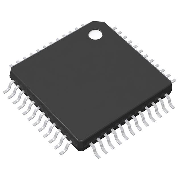
26A Group (M16C/26A, M16C/26B, M16C/26T) is housed in 42-pin and 48-pin plastic molded packages.
With a 1M byte address space, this MCU combines advanced instruction manipulation capabilities to process complex instructions by less bytes and execute instructions at higher speed. The M16C/26A Group
(M16C/26A, M16C/26B, M16C/26T) has a multiplier and DMAC adequate for office automation, communication devices and industrial equipment, and other high-speed processing applications.
1.1 Applications
Audio, cameras, office/communications/portable/ equipment, air-conditioning equipment, home appliances, etc.
Rev. 0.51 Jul.25, 2006
REJ03B0071-0051
page 1 of 26
�M16C/26A Group (M16C/26A, M16C/26B, M16C/26T)
1. Overview
1.2 Performance Outline
Table 1.1 and 1.2 outline performance overview of the M16C/26A Group (M16C/26A, M16C/26B, M16C/
26T).
Table 1.1. M16C/26A Group(M16C/26A, M16C/26B, M16C/26T) Performance (48-Pin Package)
Item
Specification
CPU
Peripheral
Function
Basic instructions
Minimun instruction
execution time
Operating mode
Address space
Memory capacity
I/O ports
Multifunction timers
Serial I/O
A/D converter
DMAC
CRC calcuration circuit
Watchdog timer
Interrupts
Clock generation circuit
Electrical
Characteristics
Oscillation stop detection
Voltage detection circuit
Power supply voltage
Power consumption
Flash Memory Programming /erasure
Version
voltage
Programming /erasure
endurance
Operating Ambient Temperature
91 instructions
41.7 ns (f(BCLK) = 24MHZ(4), VCC = 4.2 to 5.5 V)
(M16C/26B)
50 ns (f(BCLK) = 20MHZ, VCC = 3.0 to 5.5 V)
(M16C/26A, M16C/26B, M16C/26T(T-ver.))
100 ns (f(BCLK) = 10MHZ , VCC = 2.7 to 5.5 V)
(M16C/26A , M16C/26B)
50 ns (f(BCLK) = 20MHZ, VCC = 4.2 to 5.5 V -40 to 105°C)
(M16C/26T(V-ver.))
62.5 ns (f(BCLK) = 16MHZ, VCC = 4.2 to 5.5 V -40 to 125°C)
(M16C/26T(V-ver.))
Single-chip mode
1 Mbyte
See 1.4 Product Information
39 I/O pins
TimerA:16 bits x 5 channels, TimerB:16 bits x 3 channels
Three-phase motor control timer
2 channels (UART, clock synchronous serial I/O)
1 channel (UART, clock synchronous, I2C bus(1) , or IEBus(2))
10 bit A/D Converter : 1 circuit, 12 channels
2 channels
1 circuit (CRC-CCITT and CRC-16) with MSB/LSB selectable
15 bits x 1 channel (with prescaler)
20 internal and 8 external sources, 4 software sources,
Interrupt priority level: 7
4 circuits
Main clock oscillation circuit(*), Sub-clock oscillation circuit(*)
On-chip oscillator, PLL frequency synthesizer
(*)Equipped with a built-in feedback resister.
Main clock oscillation stop, re-oscillation detection function
On-chip (M16C/26A, M16C/26B), not on-chip (M16C/26T)
VCC = 4.2 to 5.5 V (f(BCLK) = 24 MHZ)(4)
(M16C/26B)
VCC = 3.0 to 5.5 V (f(BCLK) = 20 MHZ)
(M16C/26A, M16C/26B)
VCC = 2.7 to 5.5 V (f(BCLK) = 10 MHZ)
VCC = 3.0 to 5.5 V
(M16C/26T(T-ver.))
VCC = 4.2 to 5.5 V
(M16C/26T(V-ver.))
16 mA (Vcc = 5 V, f(BCLK) = 20 MHz)
25 µA (f(XCIN) = 32 KHz on RAM)
3 µA (Vcc = 3 V, f(XCIN) = 32 KHz, in wait mode)
0.7 µA (Vcc = 3 V, in stop mode)
2.7 to 5.5 V (M16C/26A, M16C/26B)
3.0 to 5.5 V (M16C/26T(T-ver.)) 4.2 to 5.5 V (M16C/26T(V-ver.))
100 times (all area) or 1,000 times (block 0 to 3)
/ 10,000 times (block A, block B)(3)
-20 to 85°C / -40 to 85°C (3)
(M16C/26A , M16C/26B)
-40 to 85°C
(M16C/26T(T-ver.))
-40 to 105°C / -40 to 125°C
(M16C/26T(V-ver.))
48-pin plastic molded QFP
Package
NOTES:
1. I2C bus is a trademark of Koninklijke Philips Electronics N. V.
2. IEBus is a trademark of NEC Electronics Corporation.
3. See Table 1.7 Product Code for the program and erase endurance, and operating ambient temperature.
4. The PLL frequency synthesizer is used to run the M16C/26B at f(BCLK) = 24 MHz.
Rev. 0.51 Jul.25, 2006
REJ03B0071-0051
page 2
of 26
�M16C/26A Group (M16C/26A, M16C/26B, M16C/26T)
1. Overview
Table 1.2. Performance outline of M16C/26A group (M16C/26A, M16C/26B) (42-pin device)
CPU
Peripheral
function
Item
Basic instructions
Minimun instruction
execution time
Operation mode
Address space
Memory capacity
Port
Multifunction timer
Serial I/O
A/D converter
DMAC
CRC calcuration circuit
Watchdog timer
Interrupt
Clock generation circuit
Electrical
Characteristics
Oscillation stop detection
Voltage detection circuit
Supply voltage
Power Consumption
Performance
91 instructions
41.7 ns (f(BCLK) = 24 MHz (4), VCC = 4.2 to 5.5 V
(M16C/26B)
50 ns (f(BCLK) = 20 MHZ, VCC = 3.0 to 5.5 V)
(M16C/26A, M16C/26B)
100 ns (f(BCLK) = 10 MHZ , VCC = 2.7 to 5.5 V)
(M16C/26A, M16C/26B)
Single-chip mode
1M byte
See 1.4 Product Information
33 I/O pins
Timer A: 16 bits x 5 channels, Timer B: 16 bits x 3 channels
Three-phase motor control timer
1 channel (UART, clock synchronous serial I/O)
1 channel (UART, clock synchronous, I2C bus(1) , or IEBus(2))
10 bit A/D converter: 1 circuit, 10 channels
2 channels
1 circuits (CRC-CCITT and CRC-16) with MSB/LSB selectable
15 bits x 1 channel (with prescaler)
18 internal and 8 external sources, 4 software sources,
Interrupt priority level: 7
4 circuits
Main clock(*), Sub-clock(*)
On-chip oscillator, PLL frequency synthesizer
(*)Equipped with a built-in feedback resister.
Main clock oscillation stop, re-oscillation detection function
On-chip
VCC = 4.2 to 5.5 V (f(BCLK) = 24 MHZ)(4)
(M16C/26B)
VCC = 3.0 to 5.5 V (f(BCLK) = 20 MHZ)
(M16C/26A, M16C/26B)
VCC = 2.7 to 5.5 V (f(BCLK) = 10 MHZ)
16 mA (Vcc = 5 V, f(BCLK) = 20 MHz)
25 µA (f(XCIN) = 32 KHz on RAM)
3 µA (Vcc = 3 V, f(XCIN) = 32 KHz, in wait mode)
0.7 µA (Vcc = 3 V, in stop mode)
2.7 to 5.5 V
Flash memory Programming/erasure
voltage
Programming/erasure
100 times (all area) or 1,000 times (block 0 to 3)
endurance
/ 10,000 times (block A, block B)(3)
Operating Ambient Temperature
-20 to 85°C / -40 to 85°C (3)
Package
42-pin plastic molded SSOP
NOTES:
1. I2C bus is a trademark of Koninklijke Philips Electronics N. V.
2. IEBus is a trademark of NEC Electronics Corporation.
3. See Table 1.7 Product Code for the program and erase endurance, and operating ambient temperature.
4. The PLL frequency synthesizer is used to run the M16C/26B at f(BCLK) = 24 MHz.
Rev. 0.51 Jul.25, 2006
REJ03B0071-0051
page 3
of 26
�1. Overview
M16C/26A Group (M16C/26A, M16C/26B, M16C/26T)
1.3 Block Diagram
Figure 1.1 and 1.2 show block diagrams of the M16C/26A Group (M16C/26A, M16C/26B, M16C/26T) 48pin package and 42-pin package.
3
8
Port P1
Port P6
8
8
4
Port P9
Port P8
Port P7
8
Port P10
Peripheral functions
Timer (16-bit)
Output (timer A): 5channels
Input (timer B): 3 channels
Clock generation circuit
UART or
clock synchronous serial I/O
(8 bits X 3 channels)
XIN-XOUT
XCIN-XCOUT
On-Chip Oscillator
PLL frequency synthesizer
Three-phase motor
control circuit
10-bit A/D converter
12 channels
M16C/60 series CPU core
R0H
R1H
Watchdog timer
(15 bits)
R0L
R1L
R2
R3
DMAC
(2 channels)
CRC calculation circuit
(CCITT, CRC-16 )
A0
A1
FB
Memory
SB
USP
ISP
INTB
PC
FLG
ROM(1)
RAM(2)
Multiplier
NOTES:
1: ROM size depends on the MCU type.
2: RAM size depends on the MCU type.
Figure 1.1 Block Diagram(48-pin Package)
Rev. 0.51 Jul.25, 2006
REJ03B0071-0051
page 4
of 26
�1. Overview
M16C/26A Group (M16C/26A, M16C/26B, M16C/26T)
3
4
Port P1
Port P6
8
8
2
Port P9
Port P8
Port P7
8
Port P10
Peripheral functions
Timer (16-bit)
Output (timer A): 5channels
Input (timer B): 3 channels
Clock generation circuit
UART or
clock synchronous serial I/O
(8 bits X 2 channels)
XIN-XOUT
XCIN-XCOUT
On-Chip Oscillator
PLL frequency synthesizer
Three-phase motor
control circuit
10-bit A/D converter
10 channels
M16C/60 series CPU core
R0H
R1H
Watchdog timer
(15 bits)
R0L
R1L
R2
R3
DMAC
(2 channels)
CRC calculation circuit
(CCITT, CRC-16 )
A0
A1
FB
Memory
SB
USP
ISP
INTB
PC
FLG
ROM(1)
RAM(2)
Multiplier
NOTES:
1: ROM size depends on the MCU type.
2: RAM size depends on the MCU type.
Figure 1.2 Block Diagram( 42-pin Package)
Rev. 0.51 Jul.25, 2006
REJ03B0071-0051
page 5
of 26
�1. Overview
M16C/26A Group (M16C/26A, M16C/26B, M16C/26T)
1.4 Product List
Tables 1.3 to 1.6 lists product information, Figure 1.3 shows a product numbering system, Table 1.7 lists
the product code, and Figure 1.4 shows the marking.
Table 1.3 M16C/26A
Current as of Jul., 2006
M30260F3AGP
(N )
ROM
Capacity
24K + 4K
M30260F6AGP
(N )
48K + 4K
2K
M30260F8AGP
(N )
64K + 4K
2K
M30263F3AFP
(N )
24K + 4K
1K
M30263F6AFP
(N )
48K + 4K
2K
M30263F8AFP
(N )
64K + 4K
2K
M30260M3A-XXXGP
(N )
24K
1K
M30260M6A-XXXGP
(N )
48K
2K
M30260M8A-XXXGP
(N )
64K
2K
M30263M3A-XXXFP
(N )
24K
1K
M30263M6A-XXXFP
(N)
48K
2K
M30263M8A-XXXFP
(N)
64K
2K
M30260F8BGP
(D)
ROM
Capacity
64K + 4 K
RAM
Capacity
2K
M30263F8BFP
(D)
64K + 4 K
2K
Type Number
RAM
Capacity
1K
Package Type
Remarks
PLQP0048KB-A (48P6Q-A)
Product Code
U3, U5, U7, U9
Flash
memory
PRSP0042GA-B (42P2R)
U5, U9
PLQP0048KB-A (48P6Q-A)
U3, U5
Mask ROM
PRSP0042GA-B (42P2R)
U5
(N): New
Table 1.4 M16C/26B
Current as of Jul., 2006
Type Number
Package Type
PLQP0048KB-A (48P6Q-A)
PRSP0042GA-B (42P2R)
Remarks
Product Code
Flash
memory
U7
U9
(D): Under development
Table 1.5 M16C/26T T-ver.
Current as of Jul., 2006
ROM
Capacity
Type Number
RAM
Capacity
M30260F3TGP
24K + 4K
1K
M30260F6TGP
48K + 4K
2K
Package Type
Remarks
Product Code
PLQP0048KB-A (48P6Q-A)
Flash
memory
U3, U7
M30260F8TGP
64K + 4K
2K
NOTE:
1. Please contact Renesas Technolog Corp. for details on Mask ROM version.
Table 1.6 M16C/26T V-ver.
Current as of Jul., 2006
M30260F3VGP
ROM
Capacity
24K + 4K
RAM
Capacity
1K
M30260F6VGP
48K + 4K
2K
Type Number
Package
Remarks
Product Code
PLQP0048KB-A (48P6Q-A)
Flash
memory
U3, U7
M30260F8VGP
64K + 4K
2K
NOTE:
1. Please contact Renesas Technolog Corp. for details on Mask ROM version.
Rev. 0.51 Jul.25, 2006
REJ03B0071-0051
page 6
of 26
�1. Overview
M16C/26A Group (M16C/26A, M16C/26B, M16C/26T)
Type No. M 3 0 2 6 0 M 8 A - XXX G P - U3
Product code:
See Tables 1.7 to 1.10
Package type:
GP: PLQP0048KB-A (48P6Q) (M16C/26A, M16C/26B, M16C/26T)
FP: PRSP0042GA-B (42P2R) (M16C/26A, M16C/26B)
ROM number:
ROM number is omitted in flash memory version
Version:
A : M16C/26A
B : M16C/26B
T : M16C/26T T-ver.
V : M16C/26T V-ver.
ROM / RAM capacity:
3: (24K+4K) bytes (Note 1) / 1K bytes
6: (48K+4K) bytes (Note 1) / 2K bytes
8: (64K+4K) bytes (Note 1) / 2K bytes
Note 1: Only flash memory version exists in "+4K bytes"
Memory type:
M: Mask ROM version
F: Flash memory version
Pin count (The value itself has no specific meaning)
M16C/26A Group
M16C Family
Figure 1.3 Product Numbering System
Rev. 0.51 Jul.25, 2006
REJ03B0071-0051
page 7
of 26
�1. Overview
M16C/26A Group (M16C/26A, M16C/26B, M16C/26T)
Table 1.7 Product Code (Flash Memory Version) - M16C/26A, M16C/26B
Product
Code
Internal ROM
(User Program Space)
Package
Program and
Erase
Endurance
U3
Temperature
Range
Internal ROM
(Data Space)
Program and
Erase
Endurance
100
U5
Temperature
Range
100
Lead free
0 to 60ºC
0 to 60ºC
U7
1,000
U9
10,000
Operating Ambient
Temperature
-40 to 85ºC
-20 to 85ºC
-40 to 85ºC
-40 to 85ºC
-20 to 85ºC
-20 to 85ºC
Table 1.8 Product Code (Mask ROM Version - M16C/26A)
Product
Code
Package
Operating Ambient
Temperature
U3
-40ºC to 85ºC
Lead free
U5
-20ºC to 85ºC
NOTE:
1. The lead contained products, D3, D5, D7, and D9 are put together with U3, U5, U7, and U9 respectively.
Lead-free products can be mounted by both conventional Sn-Pb paste and Lead-free paste (Sn-Ag-Cu
plating).
Table 1.9 Product Code (Flash Memory Version) - M16C/26T T-ver.
Internal ROM
(User Program Space)
Product
Code
Package
Programming
and erasure
endurance
U3
Temperature
range
100
Lead free
Internal ROM
(Data Space)
Programming
and erasure
endurance
100
0ºC to 60ºC
U7
Temperature
range
Operating Ambient
Temerature
1,000
-40ºC to 85ºC
-40ºC to 85ºC
10,000
Table 1.10 Product Code (Flash Memory Version) - M16C/26T V-ver.
Internal ROM
(User Program Space)
Product
Code
Package
Programming
and erasure
endurance
U3
Temperature
range
100
Lead free
U7
Rev. 0.51 Jul.25, 2006
REJ03B0071-0051
Programming
and erasure
endurance
of 26
Temperature
range
Operating Ambient
Temerature
100
0ºC to 60ºC
1,000
page 8
Internal ROM
(Data Space)
-40ºC to 125ºC
10,000
-40ºC to 125ºC
�M16C/26A Group (M16C/26A, M16C/26B, M16C/26T)
1. Overview
(1) Flash memory version, PLQP0048KB-A (48P6Q), M16C/26A, M16C/26B
0260F8A
A U3
XXXXX
Product Name : indicates M30260F8AGP
Chip Version and Product Code:
A : Indicates chip version
The first edition is shown to be blank and continues
with A and B.
U3 : Indicates Product code (see Table 1.7 Product Code)
Date Code (5 digits) fi indicates manufacturing management code
(2) Flash memory version, PRSP0042GA-B (42P2R), M16C/26A, M16C/26B
M30263F8AFP
A U3
XXXXXXX
Product Name : indicates M30263F8AFP
Chip Version and Product Code:
A : Indicates chip version
The first edition is shown to be blank and continues
with A and B.
U3 : Indicates Product code (see Table 1.7 Product Code)
Date Code (7 digits) fi indicates manufacturing management code
(3) MASK ROM version, PLQP0048KB-A (48P6Q), M16C/26A
0260M8A
001A U3
XXXXX
Product Name : indicates M30260M8AGP
ROM number, Chip Version and Product Code:
001: Indicates ROM Number
A : Indicates chip version
The first edition is shown to be blank and continues
with A and B.
U3 : Indicates Product code (see Table 1.8 Product Code)
Date Code (5 digits) fi indicates manufacturing management code
(4) MASK ROM version, PRSP0042GA-B (42P2R), M16C/26A
M30263M8A-001FP
A U3
XXXXXXX
Product Name and ROM number
M30263M8A and FP are indicated of Produnct name
001 is indicated of ROM number
Chip Version and Product Code:
A : Indicates chip version
The first edition is shown to be blank and continues
with A and B.
U3 : Indicates Product code (see Table 1.8 Product Code)
Date Code (7 digits) fi indicates manufacturing management code
Figure 1.4 Marking Diagram (M16C/26A , M16C/26B)
Rev. 0.51 Jul.25, 2006
REJ03B0071-0051
page 9
of 26
�M16C/26A Group (M16C/26A, M16C/26B, M16C/26T)
1. Overview
(1) Flash memory version, PLQP0048KB-A (48P6Q), M16C/26T T-ver.
0260F8T
A U3
XXXXX
Product Name : indicates M30260F8TGP
Chip Version and Product Code:
A : Indicates chip version
The first edition is shown to be blank and continues
with A and B.
U3 : Indicates product code (see Table 1.9 Product Code)
Date Code (5 digits) fi indicates manufacturing management code
(2) Flash memory version, PLQP0048KB-A (48P6Q), M16C/26T V-ver.
0260F8V
A U3
XXXXX
Figure 1.5 Marking Diagram (M16C/26T)
Rev. 0.51 Jul.25, 2006
REJ03B0071-0051
page 10 of 26
Product Name : indicates M30260F8VGP
Chip Version and Product Code:
A : Indicates chip version
The first edition is shown to be blank and continues
with A and B.
U3 : Indicates product code (see Table 1.10 Product Code)
Date Code (5 digits) fi indicates manufacturing management code
�1. Overview
M16C/26A Group (M16C/26A, M16C/26B, M16C/26T)
1.5 Pin Assignments
P70/TxD2/TA0OUT/SDA2/CTS1/RTS1/CTS0/CLKS1
26
25
P64/CTS1/RTS1/CTS0/CLKS1
P65/CLK1
P66/RxD1
P67/TxD1
28
27
29
31
30
P60/CTS0/RTS0
P61/CLK0
P62/RxD0
P63/TxD0
33
32
34
P15/INT3/ADTRG /IDV
P16/INT4/IDW
P17/INT5/IDU
35
36
Figures 1.6 and 1.7 show the Pin Assignments (top view).
43
18
44
17
P100/AN0
VREF
AVcc
45
16
46
15
47
14
P93/AN24
48
13
P92/TB2IN/AN32
P91/TB1IN/AN31
P90/TB0IN/AN30/CLKOUT
CNVSS
P87/XCIN
P86/XCOUT
10
8
9
7
11
19
12
20
42
P85/NMI/SD
41
6
21
RESET
XOUT
VSS
XIN
VCC
22
40
5
39
P104/AN4/KI0
P103/AN3
P102/AN2
P101/AN1
AVss
4
23
3
24
38
2
37
1
P107/AN7/KI3
P106/AN6/KI2
P105/AN5/KI1
P71/RxD2/TA0IN/SCL2/CLK1
P72/CLK2/TA1OUT/V/RxD1
P73/CTS2/RTS2/TA1IN/V/TxD1
P74/TA2OUT/W
P75/TA2IN/W
P76/TA3OUT
P77/TA3IN
P80/TA4OUT/U
P81/TA4IN/U
P82/INT0
P83/INT1
P84/INT2/ZP
Note. Set PACR2 to PACR0 bit in the PACR register
to "1002" before you input and output it after
resetting to each pin. When the PACR register
isn't set up, the input and output function of
some of the pins are disabled.
Package: PLQP0048KB-A (48P6Q)
Figure 1.6 Pin Assignment for 48-Pin Package (Top View)
Rev. 0.51 Jul.25, 2006
REJ03B0071-0051
page 11 of 26
�1. Overview
M16C/26A Group (M16C/26A, M16C/26B, M16C/26T)
Table 1.11 Pin Characteristics for 48-Pin Package
Pin
No.
Control
Pin
Port
Interrupt
Pin
Timer Pin
1
P92
TB2IN
2
P9 1
TB1IN
3
P9 0
TB0IN
4
UART Pin
Analog Pin
AN32
AN31
CLKOUT
AN30
CNVss
5
XCIN
P8 7
6
XCOUT
P8 6
7
RESET
8
XOUT
9
Vss
10
XIN
11
Vcc
12
P8 5
NMI
SD
13
P84
INT2
ZP
14
P83
INT1
15
P82
INT0
16
P81
TA4IN / U
17
P8 0
TA4OUT / U
18
P7 7
TA3IN
19
P76
TA3OUT
20
P75
TA2IN / W
21
P74
TA2OUT / W
22
P73
TA1IN / V
CTS2 / RTS2 / TXD1
23
P72
TA1OUT / V
CLK2 / RXD1
24
P71
TA0IN
RXD2 / SCL2 / CLK1
25
P70
TA0OUT
TXD2 / SDA2 / RTS1 / CTS1 / CTS0 / CLKS1
26
P67
TXD1
27
P66
R XD 1
28
P65
CLK1
29
P64
RTS1 / CTS1/ CTS0 / CLKS1
30
P63
TXD0
R XD 0
31
P62
32
P61
CLK0
33
P60
RTS0 / CTS0
34
P17
INT5
IDU
35
P16
INT4
IDW
IDV
36
P15
INT3
37
P107
KI3
AN 7
38
P106
KI2
AN 6
39
P105
KI1
AN 5
40
P104
KI0
AN 4
41
P103
AN 3
42
P102
AN 2
43
P101
AN 1
P100
AN 0
P93
AN24
44
AVss
45
46
VREF
47
AVcc
48
ADTRG
Rev. 0.51 Jul.25, 2006
REJ03B0071-0051
page 12 of 26
�1. Overview
M16C/26A Group (M16C/26A, M16C/26B, M16C/26T)
P101/AN1
P102/AN2
P103/AN3
P104/AN4/KI0
P105/AN5/KI1
P106/AN6/KI2
P107/AN7/KI3
P15/INT3/ADTRG/IDV
P16/INT4/IDW
P17/INT5/IDU
AVSS
P100/AN0
VREF
AVCC
1
42
2
41
3
40
4
39
P91/TB1IN/AN31
P90/TB0IN/AN30/CLKout
CNVSS
5
38
6
37
7
36
P87/XCIN
P86/XCOUT
8
35
9
34
RESET
XOUT
VSS
XIN
10
33
11
32
12
31
13
30
VCC
P85/NMI/SD
P84/INT2/ZP
P83/INT1
P82/INT0
14
29
15
28
16
27
17
26
18
25
P81/TA4IN/U
P80/TA4OUT/U
P77/TA3IN
19
24
20
23
P73/CTS2/RTS2/TA1IN/V/TxD1
P74/TA2OUT/W
P75/TA2IN/W
21
22
P76/TA3OUT
P64/CTS1/RTS1/CTS0/CLKS1
P65/CLK1
P66/RxD1
P67/TxD1
P70/TxD2/SDA2/TA0OUT/CTS1/RTS1/CTS0/CLKS1
P71/RxD2/SCL2/TA0IN/CLK1
P72/CLK2/TA1OUT/V/RxD1
Note. Set PACR2 to PACR0 bit in the PACR register
to "0012" before you input and output it after
resetting to each pin. When the PACR register
isn't set up, the input and output function of
some of the pins are disabled.
Package: PRSP0042GA-B (42P2R)
Figure 1.7 Pin Assignment for 42-Pin Package (Top View)
Rev. 0.51 Jul.25, 2006
REJ03B0071-0051
page 13 of 26
�1. Overview
M16C/26A Group (M16C/26A, M16C/26B, M16C/26T)
Table 1.12 Pin Characteristics for 42-Pin Package
Pin
No.
1
Control
Pin
Port
Interrupt
Pin
Timer Pin
UART Pin
Analog Pin
AVss
2
AN 0
P100
3
VREF
4
AVCC
5
P9 1
TB1IN
6
P9 0
TB0IN
7
CNVss
8
XCIN
P8 7
9
XCOUT
P8 6
10
RESET
11
XOUT
12
Vss
13
XIN
14
VCC
15
P85
NMI
SD
16
P84
INT2
ZP
17
P83
INT1
18
P82
INT0
19
P81
TA4IN / U
20
P80
TA4OUT / U
21
P77
TA3IN
22
P76
TA3OUT
AN31
CLKOUT
23
P75
TA2IN / W
24
P74
TA2OUT / W
25
P73
TA1IN / V
26
P72
TA1OUT / V
CLK2 / RXD1
27
P71
TA0IN
RXD2 / SCL2 / CLK1
28
P70
TA0OUT
TXD2 / SDA2 / RTS1 / CTS1 / CTS0 / CLKS1
AN30
CTS2 / RTS2 / TXD1
29
P67
TXD1
30
P66
R XD 1
31
P65
CLK1
32
P64
33
P17
INT5
IDU
34
P16
INT4
IDW
IDV
RTS1 / CTS1/ CTS0 / CLKS1
35
P15
INT3
36
P107
KI3
ADTRG
AN 7
37
P106
KI2
AN 6
38
P105
KI1
AN 5
39
P104
KI0
AN 4
40
P103
AN 3
41
P102
AN 2
42
P101
AN 1
Rev. 0.51 Jul.25, 2006
REJ03B0071-0051
page 14 of 26
�M16C/26A Group (M16C/26A, M16C/26B, M16C/26T)
1. Overview
1.6 Pin Description
Table 1.13 Pin Description (48-Pin and 42-Pin Packages)
Classification Pin Name
Power Supply VCC, VSS
Analog Power
Supply
Reset Input
CNVSS
Main Clock
Input
Main Clock
Output
Sub Clock Input
Sub Clock Output
Clock Output
______
INT Interrupt
Input
_______
NMI Interrupt
Input
AVCC
AVSS
____________
RESET
CNVSS
XIN
XOUT
XCIN
XCOUT
CLKOUT
________
________
INT0 to INT5
_______
NMI
_____
_____
Key Input Interrupt KI0 to KI3
Timer A
TA0OUT to
I/O Type
Description
Apply 0V to the Vss pin. Apply following voltage to the Vcc pin.
I
2.7 to 5.5 V (M16C/26A, M16C/26B), 3.0 to 5.5 V (M16C/26T T-ver.), 4.2
to 5.5 V (M16C/26T V-ver.)
Supplies power to the A/D converter. Connect the AVCC pin to VCC and
I
the AVSS pin to VSS
___________
The MCU is in a reset state when "L" is applied to the RESET pin
I
Connect the CNVSS pin to VSS
I
I/O pins for the main clock oscillation circuit. Connect a ceramic resonator
I
or crystal oscillator between XIN and XOUT. To apply external clock, apply
it
to XIN and leave XOUT open. If XIN is not used (for external oscillator or
O
external clock), connect XIN pin to VCC and leave XOUT open
I/O pins for the sub clock oscillation circuit. Connect a crystal oscillator
I
between XCIN and XCOUT
O
Outputs the clock having the same frequency as f1, f8, f32, or fC
O
______
________
Input pins for the INT interrupt. INT2 can be used for Timer A Z-phase
I
function
_______
_______
NMI interrupt input pin. NMI cannot be used as I/O port while the three-phase
I
_______
motor control is enabled. Apply a stable "H" to NMI after setting it's direction
register to "0" when the three-phase motor control is enabled
Input pins for the key input interrupt
I
I/O pins for the timer A0 to A4
I/O
TA4OUT
TA0IN to
I
Input pins for the timer A0 to A4
I
I
Input pin for Z-phase
Timer B0 to B1 input pins
O
Output pins for the three-phase motor control timer
I/O
I/O pins for the three-phase motor control timer
I
O
I/O
I
O
O
I
Input pins to control data transmission
Output pins to control data reception
Inputs and outputs the transfer clock
Inputs serial data
Outputs serial data
Output pin for transfer clock
Applies reference voltage to the A/D converter
TA4IN
ZP
Timer B
TB0IN to
TB1IN
___
Three-Phase
Motor Control
Timer Output
___
U, U, V, V,
___
W, W
IDU, IDW,
_____
IDV, SD
_________
Serial I/O
_________
CTS1 to CTS2
_________
_________
RTS1 to RTS2
CLK1 to CLK2
RxD1 to RxD2
TxD1 to TxD2
CLKS1
Reference
Voltage Input
A/D Converter
VREF
AN0 to AN7
I
Analog input pins for the A/D converter
AN30 to AN31
___________
P15 to P17
I
I/O
P64 to P67
I/O
ADTRG
I/O Ports
P70 to P77
P80 to P87
P100 to P107
Input pin for an external A/D trigger
I/O ports for CMOS. Each port can be programmed for input or output
under the control of the direction register. An input port can be set, by
program, for a pull-up resistor available or for no pull-up resister available
in 3-bit units
I/O ports for CMOS. Each port can be programmed for input or output
under the control of the direction register. An input port can be set, by
program, for a pull-up resistor available or for no pull-up resister available
in 4-bit units
P90 to P91
I : Input
O : Output
Rev. 0.51 Jul.25, 2006
REJ03B0071-0051
I/O : Input and output
page 15 of 26
�1. Overview
M16C/26A Group (M16C/26A, M16C/26B, M16C/26T)
Table 1.13 Pin Description ( 48-pin packages only) (Continued)
Classification
Pin Name
I/O Type
Description
_________
Serial I/O
CTS0
_________
RTS0
CLK0
RxD0
TxD0
Timer B
TB2IN
A/D Converter AN24
I/O Ports
AN32
P60 to P63
I
O
Inputs pin to control data transmission
Output pin to control data reception
I/O
I
Inputs and outputs the transfer clock
Inputs serial data
O
I
Outputs serial data
Timer B2 input pin
I
Analog input pins for the A/D converter
I/O
P92 to P93
I : Input
O : Output
Rev. 0.51 Jul.25, 2006
REJ03B0071-0051
I/O ports for CMOS. Each port can be programmed for input or output
under the control of the direction register. An input port can be set, by
program, for a pull-up resistor available or for no pull-up resister available
in 4-bit units
I/O : Input and output
page 16 of 26
�M16C/26A Group (M16C/26A, M16C/26B, M16C/26T)
2. CPU
2. Central Processing Unit (CPU)
Figure 2.1 shows the CPU registers. The register bank is comprised of seven registers (R0, R1, R2, R3,
A0, A1 and FB) out of 13 registers. There are two sets of register bank.
b31
b15
b8 b7
b0
R2
R0H(R0's high bits) R0L(R0's low bits)
R3
R1H(R1's high bits)R1L(R1's low bits)
R2
Data registers (Note)
R3
A0
b19
A1
Address registers (Note)
FB
Frame base registers (Note)
b15
b0
INTBH
INTBL
Interrupt table register
The upper 4 bits of INTB are INTBH and
the lower 16 bits of INTB are INTBL.
b19
b0
PC
Program counter
b15
b0
USP
User stack pointer
ISP
Interrupt stack pointer
SB
Static base register
b15
b0
FLG
b15
b8
b7
b
Flag register
b0
Carry flag
Debug flag
Zero flag
Sign flag
Register bank select flag
Overflow flag
Interrupt enable flag
Stack pointer select flag
Reserved area
Processor interrupt priority level
Reserved area
Note: These registers comprise a register bank. There are two register banks.
Figure 2.1. CPU Register
2.1 Data Registers (R0, R1, R2 and R3)
The R0 register consists of 16 bits, and is used mainly for transfers and arithmetic/logic operations. R1 to
R3 are the same as R0.
The R0 register can be separated between high (R0H) and low (R0L) for use as two 8-bit data registers.
R1H and R1L are the same as R0H and R0L. Conversely, R2 and R0 can be combined for use as a 32-bit
data register (R2R0). R3R1 is the same as R2R0.
2.2 Address Registers (A0 and A1)
The register A0 consists of 16 bits, and is used for address register indirect addressing and address register relative addressing. They also are used for transfers and arithmetic/logic operations. A1 is the same as
A0.
In some instructions, registers A1 and A0 can be combined for use as a 32-bit address register (A1A0).
Rev. 0.51 Jul.25, 2006
REJ03B0071-0051
page 17 of 26
�M16C/26A Group (M16C/26A, M16C/26B, M16C/26T)
2. CPU
2.3 Frame Base Register (FB)
FB is configured with 16 bits, and is used for FB relative addressing.
2.4 Interrupt Table Register (INTB)
INTB is configured with 20 bits, indicating the start address of an interrupt vector table.
2.5 Program Counter (PC)
PC is configured with 20 bits, indicating the address of an instruction to be executed.
2.6 User Stack Pointer (USP) and Interrupt Stack Pointer (ISP)
Stack pointer (SP) comes in two types: USP and ISP, each configured with 16 bits.
Your desired type of stack pointer (USP or ISP) can be selected by the U flag of FLG.
2.7 Static Base Register (SB)
SB is configured with 16 bits, and is used for SB relative addressing.
2.8 Flag Register (FLG)
FLG consists of 11 bits, indicating the CPU status.
2.8.1 Carry Flag (C Flag)
This flag retains a carry, borrow, or shift-out bit that has occurred in the arithmetic/logic unit.
2.8.2 Debug Flag (D Flag)
The D flag is used exclusively for debugging purpose. During normal use, it must be set to 0.
2.8.3 Zero Flag (Z Flag)
This flag is set to 1 when an arithmetic operation resulted in 0; otherwise, it is 0.
2.8.4 Sign Flag (S Flag)
This flag is set to 1 when an arithmetic operation resulted in a negative value; otherwise, it is 0.
2.8.5 Register Bank Select Flag (B Flag)
Register bank 0 is selected when this flag is 0 ; register bank 1 is selected when this flag is 1.
2.8.6 Overflow Flag (O Flag)
This flag is set to 1 when the operation resulted in an overflow; otherwise, it is 0.
2.8.7 Interrupt Enable Flag (I Flag)
This flag enables a maskable interrupt.
Maskable interrupts are disabled when the I flag is 0, and are enabled when the I flag is 1.
The I flag is cleared to 0 when the interrupt request is accepted.
2.8.8 Stack Pointer Select Flag (U Flag)
ISP is selected when the U flag is 0; USP is selected when the U flag is 1.
The U flag is cleared to 0 when a hardware interrupt request is accepted or an INT instruction for software
interrupt Nos. 0 to 31 is executed.
2.8.9 Processor Interrupt Priority Level (IPL)
IPL is configured with three bits, for specification of up to eight processor interrupt priority levels from level
0 to level 7.
If a requested interrupt has priority greater than IPL, the interrupt is enabled.
2.8.10 Reserved Area
When write to this bit, write 0. When read, its content is undefined.
Rev. 0.51 Jul.25, 2006
REJ03B0071-0051
page 18 of 26
�M16C/26A Group (M16C/26A, M16C/26B, M16C/26T)
3. Memory
3. Memory
Figure 3.1 is a memory map of the M16C/26A Group (M16C/26A, M16C/26B, M16C/26T). The M16C/26A
Group provides 1-Mbyte address space addresses 0000016 to FFFFF16.
The internal ROM is allocated lower address, beginning with address FFFFF16. For example, a 64-Kbyte
internal ROM area is allocated in addresses F000016 to FFFFF16. The flash memory version has two sets
of 2-Kbyte internal ROM area, block A and block B, for data space. These blocks are allocated addresses
F00016 to FFFF16.
The fixed interrupt vectors are allocated addresses FFFDC16 to FFFFF16 and they store the start address
of each interrupt routine.
The internal RAM is allocated higher addresses, beginning with address 0040016. For example, a 1-Kbyte
internal RAM area is allocated in addresses 0040016 to 007FF16. The internal RAM is used for temporarily
storing data. The area is also used as stacks when subroutines are called or interrupt requests are acknowledged.
The SFR is allocated addresses 0000016 to 003FF16. The peripheral function control registers are allocated here. All blank spaces within SFR location are reserved and cannot be accessed by users.
The special page vectors are allocated addresses FFE0016 to FFFDB16. They are used for the JMPS
instruction and JSRS instruction. Refer to the Renesas publication M16C/60 and M16C/20 Series Software Manual for details.
0000016
SFR
FFE0016
0040016
Internal RAM
Special page
vector table
XXXXX16
Reserved
Internal ROM
Internal RAM
Size
Address XXXXX16
Size
0F00016
Address YYYYY16
1K bytes
007FF16
24K bytes
2K bytes
00BFF16
48K bytes
F400016
64K bytes
F000016
FA00016
Internal ROM (1)
(Data space)
0FFFF16
FFFDC16
Undefined instruction
FFFFF16
BRK instruction
Address match
Single step
Watchdog timer
DBC
NMI
Reset
Overflow
Reserved
YYYYY16
(2)
Internal ROM
(Program space)
FFFFF16
NOTE:
1. Block A (2 Kbytes) and block B (2 Kbytes).
2. Do not write to the internal ROM in Mask ROM version.
Figure 3.1 Memory Map
Rev. 0.51 Jul.25, 2006
REJ03B0071-0051
page 19 of 26
�3. Memory
M16C/26A Group (M16C/26A, M16C/26B, M16C/26T)
4. Special Function Register (SFR)
Table 4.1 SFR Information(1)(1)
Register
Address
Symbol
After reset
000016
000116
000216
000316
000616
Processor mode register 0
Processor mode register 1
System clock control register 0
PM0
PM1
CM0
000716
System clock control register 1
CM1
0016
000010002
010010002(M16C/26A)
011010002(M16C/26T)
001000002
Address match interrupt enable register
Protect register
AIER
PRCR
XXXXXX002
XX0000002
Oscillation stop detection register(2)
CM2
0X0000002
Watchdog timer start register
Watchdog timer control register
Address match interrupt register 0
WDTS
WDC
RMAD0
XX16
00XXXXXX2 (3)
0016
0016
X016
Address match interrupt register 1
RMAD1
0016
0016
X016
Voltage detection register 1 (4, 5)
Voltage detection register 2 (4, 5)
VCR1
VCR2
000010002
0016
PLL control register 0
PLC0
0001X0102
Processor mode register 2
Low voltage detection interrupt register(5)
DMA0 source pointer
PM2
D4INT
SAR0
XXX000002
0016
XX16
XX16
XX16
DMA0 destination pointer
DAR0
XX16
XX16
XX16
DMA0 transfer counter
TCR0
XX16
XX16
DMA0 control register
DM0CON
00000X002
DMA1 source pointer
SAR1
XX16
XX16
XX16
DMA1 destination pointer
DAR1
XX16
XX16
XX16
DMA1 transfer counter
TCR1
XX16
XX16
DMA1 control register
DM1CON
00000X002
000416
000516
000816
000916
000A16
000B16
000C16
000D16
000E16
000F16
001016
001116
001216
001316
001416
001516
001616
001716
001816
001916
001A16
001B16
001C16
001D16
001E16
001F16
002016
002116
002216
002316
002416
002516
002616
002716
002816
002916
002A16
002B16
002C16
002D16
002E16
002F16
003016
003116
003216
003316
003416
003516
003616
003716
003816
003916
003A16
003B16
003C16
003D16
003E16
003F16
NOTES:
1. The blank spaces are reserved. No access is allowed.
2. Bits CM27, CM21, and CM20 do not change at oscillation stop detection reset.
3. The WDC5 bit is 0 (cold start) immediately after power-on. It can only be set to 1 by program. The WDC5 bit cannot be used in
M16C/26T.
4. The VCR1 and VCR2 registers do not change at software reset, watchdog timer reset, and oscillation stop detection reset.
5. Registers VCR1, VCR2, and D4INT cannot be used in M16C/26T.
X : Undefined
Rev. 0.51 Jul.25, 2006
REJ03B0071-0051
page 20 of 26
�M16C/26A Group (M16C/26A, M16C/26B, M16C/26T)
3. Memory
Table 4.2 SFR Information(2)(1)
Address
Register
Symbol
After reset
INT3 interrupt control register
INT3IC
XX00X0002
INT5 interrupt control register
INT4 interrupt control register
UART2 Bus collision detection interrupt control register
DMA0 interrupt control register
DMA1 interrupt control register
Key input interrupt control register
A/D conversion interrupt control register
UART2 transmit interrupt control register
UART2 receive interrupt control register
UART0 transmit interrupt control register
UART0 receive interrupt control register
UART1 transmit interrupt control register
UART1 receive interrupt control register
TimerA0 interrupt control register
TimerA1 interrupt control register
TimerA2 interrupt control register
TimerA3 interrupt control register
TimerA4 interrupt control register
TimerB0 interrupt control register
TimerB1 interrupt control register
TimerB2 interrupt control register
INT0 interrupt control register
INT1 interrupt control register
INT2 interrupt control register
INT5IC
INT4IC
BCNIC
DM0IC
DM1IC
KUPIC
ADIC
S2TIC
S2RIC
S0TIC
S0RIC
S1TIC
S1RIC
TA0IC
TA1IC
TA2IC
TA3IC
TA4IC
TB0IC
TB1IC
TB2IC
INT0IC
INT1IC
INT2IC
XX00X0002
XX00X0002
XXXXX0002
XXXXX0002
XXXXX0002
XXXXX0002
XXXXX0002
XXXXX0002
XXXXX0002
XXXXX0002
XXXXX0002
XXXXX0002
XXXXX0002
XXXXX0002
XXXXX0002
XXXXX0002
XXXXX0002
XXXXX0002
XXXXX0002
XXXXX0002
XXXXX0002
XX00X0002
XX00X0002
XX00X0002
004016
004116
004216
004316
004416
004516
004616
004716
004816
004916
004A16
004B16
004C16
004D16
004E16
004F16
005016
005116
005216
005316
005416
005516
005616
005716
005816
005916
005A16
005B16
005C16
005D16
005E16
005F16
006016
006116
006216
006316
006416
006516
006616
006716
006816
006916
006A16
006B16
006C16
006D16
006E16
006F16
007016
007116
007216
007316
007416
007516
007616
007716
007816
007916
007A16
007B16
007C16
007D16
007E16
007F16
NOTE:
1. Blank spaces are reserved. No access is allowed.
X: Undefined
Rev. 0.51 Jul.25, 2006
REJ03B0071-0051
page 21 of 26
�3. Memory
M16C/26A Group (M16C/26A, M16C/26B, M16C/26T)
Table 4.3 SFR Information(3)(1)
Address
Register
Symbol
After reset
008016
008116
008216
008316
008416
008516
008616
~
~
~
~
01B016
01B116
01B216
01B316
Flash memory control register 4
(Note 2)
FMR4
010000002
Flash memory control register 1
(Note 2)
FMR1
000XXX0X2
Flash memory control register 0
(Note 2)
FMR0
0116
01B416
01B516
01B616
01B716
01B816
01B916
01BA16
01BB16
01BC16
01BD16
01BE16
01BF16
~
~
~
~
025016
025116
025216
025316
025416
025516
025616
025716
025816
025916
025A16
Three phase protect control register
TPRC
0016
On-chip oscillator control register
Pin assignment control register
Peripheral clock select register
ROCR
PACR
PCLKR
000001012
0016
000000112
025B16
025C16
025D16
025E16
025F16
~
~
~
~
033016
033116
033216
033316
033416
033516
033616
033716
033816
033916
033A16
033B16
033C16
033D16
033E16
033F16
NMI digital debounce register
Port17 digital debounce register
NOTES:
1. Blank spaces are reserved. No access is allowed.
2. This register is included in the flash memory version.
X: Undefined
Rev. 0.51 Jul.25, 2006
REJ03B0071-0051
page 22 of 26
NDDR
P17DDR
FF16
FF16
�M16C/26A Group (M16C/26A, M16C/26B, M16C/26T)
3. Memory
Table 4.4 SFR Information(4)(1)
Address
Register
Symbol
After reset
034016
034116
034216
Timer A1-1 register
TA11
Timer A2-1 register
TA21
Timer A4-1 register
TA41
Three phase PWM control register 0
Three phase PWM control register 1
Three phase output buffer register 0
Three phase output buffer register 1
Dead time timer
Timer B2 Interrupt occurrence frequency set counter
Position-data-retain function control register
INVC0
INVC1
IDB0
IDB1
DTT
ICTB2
PDRF
XX16
XX16
XX16
XX16
XX16
XX16
0016
0016
3F16
3F16
XX16
XX16
XXXX00002
Port function control register
PFCR
001111112
Interrupt request cause select register 2
Interrupt request cause select register
IFSR2A
IFSR
XXXXXXX02
0016
UART2 special mode register 4
UART2 special mode register 3
UART2 special mode register 2
UART2 special mode register
UART2 transmit/receive mode register
UART2 bit rate register
UART2 transmit buffer register
U2SMR4
U2SMR3
U2SMR2
U2SMR
U2MR
U2BRG
U2TB
UART2 transmit/receive control register 0
UART2 transmit/receive control register 1
UART2 receive buffer register
U2C0
U2C1
U2RB
0016
000X0X0X2
X00000002
X00000002
0016
XX16
XXXXXXXX2
XXXXXXXX2
000010002
000000102
XXXXXXXX2
XXXXXXXX2
034316
034416
034516
034616
034716
034816
034916
034A16
034B16
034C16
034D16
034E16
034F16
035016
035116
035216
035316
035416
035516
035616
035716
035816
035916
035A16
035B16
035C16
035D16
035E16
035F16
036016
036116
036216
036316
036416
036516
036616
036716
036816
036916
036A16
036B16
036C16
036D16
036E16
036F16
037016
037116
037216
037316
037416
037516
037616
037716
037816
037916
037A16
037B16
037C16
037D16
037E16
037F16
NOTE:
1. Blank spaces are reserved. No access is allowed.
X : Undefined
Rev. 0.51 Jul.25, 2006
REJ03B0071-0051
page 23 of 26
�3. Memory
M16C/26A Group (M16C/26A, M16C/26B, M16C/26T)
Table 4.5 SFR Information(5)(1)
Address
038016
038116
038216
038316
038416
Count start flag
Clock prescaler reset flag
One-shot start flag
Trigger select register
Up-dowm flag
Register
Symbol
TABSR
CPSRF
ONSF
TRGSR
UDF
After reset
0016
0XXXXXXX2
0016
0016
0016
Timer A0 register
TA0
Timer A1 register
TA1
Timer A2 register
TA2
Timer A3 register
TA3
Timer A4 register
TA4
Timer B0 register
TB0
Timer B1 register
TB1
Timer B2 register
TB2
Timer A0 mode register
Timer A1 mode register
Timer A2 mode register
Timer A3 mode register
Timer A4 mode register
Timer B0 mode register
Timer B1 mode register
Timer B2 mode register
Timer B2 special mode register
TA0MR
TA1MR
TA2MR
TA3MR
TA4MR
TB0MR
TB1MR
TB2MR
TB2SC
XX16
XX16
XX16
XX16
XX16
XX16
XX16
XX16
XX16
XX16
XX16
XX16
XX16
XX16
XX16
XX16
0016
0016
0016
0016
0016
00XX00002
00XX00002
00XX00002
X00000002
UART0 transmit/receive mode register
UART0 bit rate register
UART0 transmit buffer register
U0MR
U0BRG
U0TB
UART0 transmit/receive control register 0
UART0 transmit/receive control register 1
UART0 receive buffer register
U0C0
U0C1
U0RB
UART1 transmit/receive mode register
UART1 bit rate register
UART1 transmit buffer register
U1MR
U1BRG
U1TB
UART1 transmit/receive control register 0
UART1 transmit/receive control register 1
UART1 receive buffer register
U1C0
U1C1
U1RB
UART transmit/receive control register 2
UCON
CRC snoop address register
CRCSAR
CRC mode register
CRCMR
XX16
00XXXXXX2
0XXXXXX02
DMA0 request cause select register
DM0SL
0016
DMA1 request cause select register
DM1SL
0016
CRC data register
CRCD
CRC input register
CRCIN
XX16
XX16
XX16
038516
038616
038716
038816
038916
038A16
038B16
038C16
038D16
038E16
038F16
039016
039116
039216
039316
039416
039516
039616
039716
039816
039916
039A16
039B16
039C16
039D16
039E16
039F16
03A016
03A116
03A216
03A316
03A416
03A516
03A616
03A716
03A816
03A916
03AA16
03AB16
03AC16
03AD16
03AE16
03AF16
03B016
0016
XX16
XXXXXXXX2
XXXXXXXX2
000010002
000000102
XXXXXXXX2
XXXXXXXX2
0016
XX16
XXXXXXXX2
XXXXXXXX2
000010002
000000102
XXXXXXXX2
XXXXXXXX2
X00000002
03B116
03B216
03B316
03B416
03B516
03B616
03B716
03B816
03B916
03BA16
03BB16
03BC16
03BD16
03BE16
03BF16
NOTE:
1. Blank spaces are reserved. No access is allowed.
X : Undefined
Rev. 0.51 Jul.25, 2006
REJ03B0071-0051
page 24 of 26
�M16C/26A Group (M16C/26A, M16C/26B, M16C/26T)
3. Memory
Table 4.6 SFR Information(6)(1)
Register
Address
03C016
A/D register 0
Symbol
AD0
A/D register 1
AD1
A/D register 2
AD2
A/D register 3
AD3
A/D register 4
AD4
A/D register 5
AD5
A/D register 6
AD6
A/D register 7
AD7
03C116
03C216
03C316
03C416
03C516
03C616
03C716
03C816
03C916
03CA16
03CB16
03CC16
03CD16
03CE16
03CF16
After Reset
XXXXXXXX2
XXXXXXXX2
XXXXXXXX2
XXXXXXXX2
XXXXXXXX2
XXXXXXXX2
XXXXXXXX2
XXXXXXXX2
XXXXXXXX2
XXXXXXXX2
XXXXXXXX2
XXXXXXXX2
XXXXXXXX2
XXXXXXXX2
XXXXXXXX2
XXXXXXXX2
03D016
03D116
03D216
03D316
03D416
A/D trigger control register
A/D status register 0
A/D control register 2
ADTRGCON
ADSTAT0
ADCON2
0016
00000X002
0016
A/D control register 0
A/D control register 1
ADCON0
ADCON1
00000XXX2
0016
Port P1 register
P1
XX16
Port P1 direction register
PD1
0016
Port P6 register
Port P7 register
Port P6 direction register
Port P7 direction register
Port P8 register
Port P9 register
Port P8 direction register
Port P9 direction register
Port P10 register
P6
P7
PD6
PD7
P8
P9
PD8
PD9
P10
XX16
XX16
0016
0016
XX16
XXXXXXXX2
0016
XXXX00002
XX16
Port P10 direction register
PD10
0016
Pull-up control register 0
Pull-up control register 1
Pull-up control register 2
Port control register
PUR0
PUR1
PUR2
PCR
0016
0016
0016
0016
03D516
03D616
03D716
03D816
03D916
03DA16
03DB16
03DC16
03DD16
03DE16
03DF16
03E016
03E116
03E216
03E316
03E416
03E516
03E616
03E716
03E816
03E916
03EA16
03EB16
03EC16
03ED16
03EE16
03EF16
03F016
03F116
03F216
03F316
03F416
03F516
03F616
03F716
03F816
03F916
03FA16
03FB16
03FC16
03FD16
03FE16
03FF16
NOTE:
1. Blank spaces are reserved. No access is allowed.
X: Undefined
Rev. 0.51 Jul.25, 2006
REJ03B0071-0051
page 25 of 26
�Package
M16C/26A Group (M16C/26A, M16C/26B, M16C/26T)
Package
JEITA Package Code
P-LQFP48-7x7-0.50
RENESAS Code
PLQP0048KB-A
Previous Code
48P6Q-A
MASS[Typ.]
0.2g
HD
*1
D
36
25
NOTE)
1. DIMENSIONS "*1" AND "*2"
37
24
2.
DIMENSION "*3" DOES NOT
INCLUDE TRIM OFFSET.
bp
c
c1
HE
*2
E
b1
Reference Dimension in Millimeters
Symbol
D
E
A
HD
48
13
1
ZE
Terminal cross section
E
12
Index mark
ZD
A1
c
A
p
A2
F
A1
L
b1
c
c1
L1
y
*3
e
JEITA Package Code
P-SSOP42-8.4x17.5-0.80
e
x
y
ZD
ZE
L
L1
Detail F
p
RENESAS Code
PRSP0042GA-B
Previous Code
42P2R-E
Min
6.9
6.9
Nom Max
7.0 7.1
7.0 7.1
8.8
8.8
9.0
9.2
1.7
0
0.1 0.2
0.17 0.22 0.27
0.20
0.09 0.145 0.20
0.125
0º
8º
0.5
0.08
0.10
0.75
0.75
0.35 0.5 0.65
1.0
MASS[Typ.]
0.6g
E
*1
HE
42
F
NOTE)
1. DIMENSIONS "*1" AND "*2"
2. DIMENSION "*3" DOES NOT
INCLUDE TRIM OFFSET.
1
A2
Index mark
A1
c
Reference
Symbol
*2
L
A
D
e
y
bp
Detail F
D
E
A2
A
A1
bp
c
HE
e
y
L
Rev. 0.51 Jul.25, 2006
REJ03B0071-0051
page 26 of 26
Min Nom Max
17.3 17.5 17.7
8.2 8.4 8.6
2.0
2.4
0.05
0.25 0.3 0.4
0.13 0.15 0.2
0º
10º
11.63 11.93 12.23
0.65 0.8 0.95
0.15
0.3 0.5 0.7
�REVISION HISTORY
Rev.
M16C/26A Group (M16C/26A, M16C/26B, M16C/26T) Shortsheet
Date
Description
Summary
Page
0.51
07/25/06
-
First edition
A-1
�Sales Strategic Planning Div.
Nippon Bldg., 2-6-2, Ohte-machi, Chiyoda-ku, Tokyo 100-0004, Japan
Keep safety first in your circuit designs!
1. Renesas Technology Corp. puts the maximum effort into making semiconductor products better and more reliable, but there is always the possibility that trouble
may occur with them. Trouble with semiconductors may lead to personal injury, fire or property damage.
Remember to give due consideration to safety when making your circuit designs, with appropriate measures such as (i) placement of substitutive, auxiliary
circuits, (ii) use of nonflammable material or (iii) prevention against any malfunction or mishap.
Notes regarding these materials
1. These materials are intended as a reference to assist our customers in the selection of the Renesas Technology Corp. product best suited to the customer's
application; they do not convey any license under any intellectual property rights, or any other rights, belonging to Renesas Technology Corp. or a third party.
2. Renesas Technology Corp. assumes no responsibility for any damage, or infringement of any third-party's rights, originating in the use of any product data,
diagrams, charts, programs, algorithms, or circuit application examples contained in these materials.
3. All information contained in these materials, including product data, diagrams, charts, programs and algorithms represents information on products at the time of
publication of these materials, and are subject to change by Renesas Technology Corp. without notice due to product improvements or other reasons. It is
therefore recommended that customers contact Renesas Technology Corp. or an authorized Renesas Technology Corp. product distributor for the latest product
information before purchasing a product listed herein.
The information described here may contain technical inaccuracies or typographical errors.
Renesas Technology Corp. assumes no responsibility for any damage, liability, or other loss rising from these inaccuracies or errors.
Please also pay attention to information published by Renesas Technology Corp. by various means, including the Renesas Technology Corp. Semiconductor
home page (http://www.renesas.com).
4. When using any or all of the information contained in these materials, including product data, diagrams, charts, programs, and algorithms, please be sure to
evaluate all information as a total system before making a final decision on the applicability of the information and products. Renesas Technology Corp. assumes
no responsibility for any damage, liability or other loss resulting from the information contained herein.
5. Renesas Technology Corp. semiconductors are not designed or manufactured for use in a device or system that is used under circumstances in which human life
is potentially at stake. Please contact Renesas Technology Corp. or an authorized Renesas Technology Corp. product distributor when considering the use of a
product contained herein for any specific purposes, such as apparatus or systems for transportation, vehicular, medical, aerospace, nuclear, or undersea repeater
use.
6. The prior written approval of Renesas Technology Corp. is necessary to reprint or reproduce in whole or in part these materials.
7. If these products or technologies are subject to the Japanese export control restrictions, they must be exported under a license from the Japanese government and
cannot be imported into a country other than the approved destination.
Any diversion or reexport contrary to the export control laws and regulations of Japan and/or the country of destination is prohibited.
8. Please contact Renesas Technology Corp. for further details on these materials or the products contained therein.
http://www.renesas.com
RENESAS SALES OFFICES
Refer to "http://www.renesas.com/en/network" for the latest and detailed information.
Renesas Technology America, Inc.
450 Holger Way, San Jose, CA 95134-1368, U.S.A
Tel: (408) 382-7500, Fax: (408) 382-7501
Renesas Technology Europe Limited
Dukes Meadow, Millboard Road, Bourne End, Buckinghamshire, SL8 5FH, U.K.
Tel: (1628) 585-100, Fax: (1628) 585-900
Renesas Technology (Shanghai) Co., Ltd.
Unit 204, 205, AZIACenter, No.1233 Lujiazui Ring Rd, Pudong District, Shanghai, China 200120
Tel: (21) 5877-1818, Fax: (21) 6887-7898
Renesas Technology Hong Kong Ltd.
7th Floor, North Tower, World Finance Centre, Harbour City, 1 Canton Road, Tsimshatsui, Kowloon, Hong Kong
Tel: 2265-6688, Fax: 2730-6071
Renesas Technology Taiwan Co., Ltd.
10th Floor, No.99, Fushing North Road, Taipei, Taiwan
Tel: (2) 2715-2888, Fax: (2) 2713-2999
Renesas Technology Singapore Pte. Ltd.
1 Harbour Front Avenue, #06-10, Keppel Bay Tower, Singapore 098632
Tel: 6213-0200, Fax: 6278-8001
Renesas Technology Korea Co., Ltd.
Kukje Center Bldg. 18th Fl., 191, 2-ka, Hangang-ro, Yongsan-ku, Seoul 140-702, Korea
Tel: (2) 796-3115, Fax: (2) 796-2145
Renesas Technology Malaysia Sdn. Bhd
Unit 906, Block B, Menara Amcorp, Amcorp Trade Centre, No.18, Jalan Persiaran Barat, 46050 Petaling Jaya, Selangor Darul Ehsan, Malaysia
Tel: 7955-9390, Fax: 7955-9510
© 2006. Renesas Technology Corp., All rights reserved. Printed in Japan.
Colophon .6.0
�


 工商网监
湘ICP备2023018690号
工商网监
湘ICP备2023018690号
