To our customers,
Old Company Name in Catalogs and Other Documents
On April 1st, 2010, NEC Electronics Corporation merged with Renesas Technology
Corporation, and Renesas Electronics Corporation took over all the business of both
companies. Therefore, although the old company name remains in this document, it is a valid
Renesas Electronics document. We appreciate your understanding.
Renesas Electronics website: http://www.renesas.com
April 1st, 2010
Renesas Electronics Corporation
Issued by: Renesas Electronics Corporation (http://www.renesas.com)
Send any inquiries to http://www.renesas.com/inquiry.
�Notice
1.
2.
3.
4.
5.
6.
7.
All information included in this document is current as of the date this document is issued. Such information, however, is
subject to change without any prior notice. Before purchasing or using any Renesas Electronics products listed herein, please
confirm the latest product information with a Renesas Electronics sales office. Also, please pay regular and careful attention to
additional and different information to be disclosed by Renesas Electronics such as that disclosed through our website.
Renesas Electronics does not assume any liability for infringement of patents, copyrights, or other intellectual property rights
of third parties by or arising from the use of Renesas Electronics products or technical information described in this document.
No license, express, implied or otherwise, is granted hereby under any patents, copyrights or other intellectual property rights
of Renesas Electronics or others.
You should not alter, modify, copy, or otherwise misappropriate any Renesas Electronics product, whether in whole or in part.
Descriptions of circuits, software and other related information in this document are provided only to illustrate the operation of
semiconductor products and application examples. You are fully responsible for the incorporation of these circuits, software,
and information in the design of your equipment. Renesas Electronics assumes no responsibility for any losses incurred by
you or third parties arising from the use of these circuits, software, or information.
When exporting the products or technology described in this document, you should comply with the applicable export control
laws and regulations and follow the procedures required by such laws and regulations. You should not use Renesas
Electronics products or the technology described in this document for any purpose relating to military applications or use by
the military, including but not limited to the development of weapons of mass destruction. Renesas Electronics products and
technology may not be used for or incorporated into any products or systems whose manufacture, use, or sale is prohibited
under any applicable domestic or foreign laws or regulations.
Renesas Electronics has used reasonable care in preparing the information included in this document, but Renesas Electronics
does not warrant that such information is error free. Renesas Electronics assumes no liability whatsoever for any damages
incurred by you resulting from errors in or omissions from the information included herein.
Renesas Electronics products are classified according to the following three quality grades: “Standard”, “High Quality”, and
“Specific”. The recommended applications for each Renesas Electronics product depends on the product’s quality grade, as
indicated below. You must check the quality grade of each Renesas Electronics product before using it in a particular
application. You may not use any Renesas Electronics product for any application categorized as “Specific” without the prior
written consent of Renesas Electronics. Further, you may not use any Renesas Electronics product for any application for
which it is not intended without the prior written consent of Renesas Electronics. Renesas Electronics shall not be in any way
liable for any damages or losses incurred by you or third parties arising from the use of any Renesas Electronics product for an
application categorized as “Specific” or for which the product is not intended where you have failed to obtain the prior written
consent of Renesas Electronics. The quality grade of each Renesas Electronics product is “Standard” unless otherwise
expressly specified in a Renesas Electronics data sheets or data books, etc.
“Standard”:
8.
9.
10.
11.
12.
Computers; office equipment; communications equipment; test and measurement equipment; audio and visual
equipment; home electronic appliances; machine tools; personal electronic equipment; and industrial robots.
“High Quality”: Transportation equipment (automobiles, trains, ships, etc.); traffic control systems; anti-disaster systems; anticrime systems; safety equipment; and medical equipment not specifically designed for life support.
“Specific”:
Aircraft; aerospace equipment; submersible repeaters; nuclear reactor control systems; medical equipment or
systems for life support (e.g. artificial life support devices or systems), surgical implantations, or healthcare
intervention (e.g. excision, etc.), and any other applications or purposes that pose a direct threat to human life.
You should use the Renesas Electronics products described in this document within the range specified by Renesas Electronics,
especially with respect to the maximum rating, operating supply voltage range, movement power voltage range, heat radiation
characteristics, installation and other product characteristics. Renesas Electronics shall have no liability for malfunctions or
damages arising out of the use of Renesas Electronics products beyond such specified ranges.
Although Renesas Electronics endeavors to improve the quality and reliability of its products, semiconductor products have
specific characteristics such as the occurrence of failure at a certain rate and malfunctions under certain use conditions. Further,
Renesas Electronics products are not subject to radiation resistance design. Please be sure to implement safety measures to
guard them against the possibility of physical injury, and injury or damage caused by fire in the event of the failure of a
Renesas Electronics product, such as safety design for hardware and software including but not limited to redundancy, fire
control and malfunction prevention, appropriate treatment for aging degradation or any other appropriate measures. Because
the evaluation of microcomputer software alone is very difficult, please evaluate the safety of the final products or system
manufactured by you.
Please contact a Renesas Electronics sales office for details as to environmental matters such as the environmental
compatibility of each Renesas Electronics product. Please use Renesas Electronics products in compliance with all applicable
laws and regulations that regulate the inclusion or use of controlled substances, including without limitation, the EU RoHS
Directive. Renesas Electronics assumes no liability for damages or losses occurring as a result of your noncompliance with
applicable laws and regulations.
This document may not be reproduced or duplicated, in any form, in whole or in part, without prior written consent of Renesas
Electronics.
Please contact a Renesas Electronics sales office if you have any questions regarding the information contained in this
document or Renesas Electronics products, or if you have any other inquiries.
(Note 1) “Renesas Electronics” as used in this document means Renesas Electronics Corporation and also includes its majorityowned subsidiaries.
(Note 2) “Renesas Electronics product(s)” means any product developed or manufactured by or for Renesas Electronics.
�To all our customers
Regarding the change of names mentioned in the document, such as Mitsubishi
Electric and Mitsubishi XX, to Renesas Technology Corp.
The semiconductor operations of Hitachi and Mitsubishi Electric were transferred to Renesas
Technology Corporation on April 1st 2003. These operations include microcomputer, logic, analog
and discrete devices, and memory chips other than DRAMs (flash memory, SRAMs etc.)
Accordingly, although Mitsubishi Electric, Mitsubishi Electric Corporation, Mitsubishi
Semiconductors, and other Mitsubishi brand names are mentioned in the document, these names
have in fact all been changed to Renesas Technology Corp. Thank you for your understanding.
Except for our corporate trademark, logo and corporate statement, no changes whatsoever have been
made to the contents of the document, and these changes do not constitute any alteration to the
contents of the document itself.
Note : Mitsubishi Electric will continue the business operations of high frequency & optical devices
and power devices.
Renesas Technology Corp.
Customer Support Dept.
April 1, 2003
�MITSUBISHI MICROCOMPUTERS
3822 Group
SINGLE-CHIP 8-BIT CMOS MICROCOMPUTER
DESCRIPTION
The 3822 group is the 8-bit microcomputer based on the 740 family core technology.
The 3822 group has the LCD drive control circuit, an 8-channel
A-D converter, and a serial I/O as additional functions.
The various microcomputers in the 3822 group include variations
of internal memory size and packaging. For details, refer to the
section on part numbering.
For details on availability of microcomputers in the 3822 group, refer to the section on group expansion.
FEATURES
●Basic machine-language instructions ...................................... 71
●The minimum instruction execution time ........................... 0.5 µs
(at 8 MHz oscillation frequency)
●Memory size
ROM ................................................................. 4 K to 48 K bytes
RAM ................................................................. 192 to 1024 bytes
●Programmable input/output ports ............................................ 49
●Software pull-up/pull-down resistors (Ports P0-P7 except port P40 )
●Interrupts ................................................. 17 sources, 16 vectors
(includes key input interrupt)
●Timers ........................................................... 8-bit ✕ 3, 16-bit ✕ 2
●Serial I/O ...................... 8-bit ✕ 1 (UART or Clock-synchronized)
●A-D converter ................................................. 8-bit ✕ 8 channels
●LCD drive control circuit
Bias ................................................................................... 1/2, 1/3
Duty ........................................................................... 1/2, 1/3, 1/4
Common output .......................................................................... 4
Segment output ........................................................................ 32
●2 clock generating circuits
(connect to external ceramic resonator or quartz-crystal oscillator)
●Power source voltage
In high-speed mode .................................................. 4.0 to 5.5 V
In middle-speed mode ............................................... 2.5 to 5.5 V
(Extended operating temperature version:
2.0 to 5.5 V, Ta= – 20 to 85°C
3.0 to 5.5 V, Ta= – 40 to – 20°C)
(One time PROM version: 2.5 to 5.5 V)
(M version: 2.2 to 5.5 V)
(H version: 2.0 to 5.5 V)
In low-speed mode .................................................... 2.5 to 5.5 V
(Extended operating temperature version:
2.0 to 5.5 V, Ta= – 20 to 85°C
3.0 to 5.5 V, Ta= – 40 to – 20°C)
(One time PROM version: 2.5 to 5.5 V)
(M version: 2.2 to 5.5 V)
(H version: 2.0 to 5.5 V)
●Power dissipation
In high-speed mode .......................................................... 32 mW
(at 8 MHz oscillation frequency, at 5 V power source voltage)
In low-speed mode ............................................................ 45 µW
(at 32 kHz oscillation frequency, at 3 V power source voltage)
●Operating temperature range................................... – 20 to 85°C
(Extended operating temperature version: – 40 to 85 °C)
APPLICATIONS
Camera, household appliances, consumer electronics, etc.
SEG8
SEG9
SEG10
SEG11
P34/SEG12
P35/SEG13
P36/SEG14
P37/SEG15
P00/SEG16
P01/SEG17
P02/SEG18
P03/SEG19
P04/SEG20
P05/SEG21
P06/SEG22
P07/SEG23
P10/SEG24
P11/SEG25
P12/SEG26
P13/SEG27
P14/SEG28
P15/SEG29
P16/SEG30
P17/SEG31
PIN CONFIGURATION (TOP VIEW)
64 63 62 61 60 59 58 57 56 55 54 53 52 51 50 49 48 47 46 45 44 43 42 41
SEG7
SEG6
SEG5
SEG4
SEG3
SEG2
SEG1
SEG0
VCC
VREF
AVSS
COM3
COM2
COM1
COM0
VL3
65
66
67
68
40
39
38
37
36
35
34
69
70
71
72
73
74
75
M38224M6HXXXFP
76
77
78
79
80
33
32
31
30
29
28
27
26
25
P20
P21
P22
P23
P24
P25
P26
P27
VSS
XOUT
XIN
P70/XCOUT
P71/XCIN
RESET
P40
P41/φ
VL2
VL1
P67/AN7
P66/AN6
P65/AN5
P64/AN4
P63/AN3
P62/AN2
P61/AN1
P60/AN0
P57/ADT
P56/TOUT
P55/CNTR1
P54/CNTR0
P53/RTP1
P52/RTP0
P51/INT3
P50/INT2
P47/SRDY
P46/SCLK
P45/TXD
P44/RXD
P43/INT1
P42/INT0
1 2 3 4 5 6 7 8 9 10 11 12 13 14 15 16 17 18 19 20 21 22 23 24
Package type : 80P6N-A (80-pin plastic-molded QFP)
Fig. 1 M38224M6HXXXFP pin configuration
(The pin configuration of 80D0 is same as this.)
�MITSUBISHI MICROCOMPUTERS
3822 Group
SINGLE-CHIP 8-BIT CMOS MICROCOMPUTER
42
41
44
43
47
46
45
49
48
52
51
50
54
53
55
57
56
40
39
61
62
63
38
37
36
35
64
65
66
67
68
34
33
32
31
30
29
28
27
M38223M4MXXXGP
M38224M6HXXXHP
69
70
71
72
73
74
75
26
25
24
23
76
77
78
79
80
20
19
18
17
15
16
13
14
12
10
11
7
8
9
5
6
P67/AN7
P66/AN6
P65/AN5
P64/AN4
P63/AN3
P62/AN2
P61/AN1
P60/AN0
P57/ADT
P56/TOUT
P55/CNTR1
P54/CNTR0
P53/RTP1
P52/RTP0
P51/INT3
P50/INT2
P47/SRDY
P46/SCLK
P45/TXD
P44/RXD
2
3
4
22
21
1
SEG9
SEG8
SEG7
SEG6
SEG5
SEG4
SEG3
SEG2
SEG1
SEG0
VCC
VREF
AVSS
COM3
COM2
COM1
COM0
VL3
VL2
VL1
59
58
60
SEG10
SEG11
P34/SEG12
P35/SEG13
P36/SEG14
P37/SEG15
P00/SEG16
P01/SEG17
P02/SEG18
P03/SEG19
P04/SEG20
P05/SEG21
P06/SEG22
P07/SEG23
P10/SEG24
P11/SEG25
P12/SEG26
P13/SEG27
P14/SEG28
P15/SEG29
PIN CONFIGURATION (TOP VIEW)
Package type : 80P6S-A/80P6Q-A
(80-pin plastic-molded QFP)
Fig. 2 M38223M4MXXXGP/M38224M6HXXXHP pin configuration
2
P16/SEG30
P17/SEG31
P20
P21
P22
P23
P24
P25
P26
P27
VSS
XOUT
XIN
P70/XCOUT
P71/XCIN
RESET
P40
P41/φ
P42/INT0
P43/INT1
�XCIN
I/O Port P7
26 27
P7(2)
XCOUT
1
2
5
6
7
I/O Port P6
3 4
P6(8)
XCIN
XCOUT
φ
Sub-Clock Sub-Clock
Input
Output
Clock generating
circuit
8
VREF
AVSS
(0V)
7 2 73
A-D
converter(8)
ADT
9
P5(8)
CNTR0,CNTR1
TOUT
PS
PCL
S
Y
X
A
I/O Port P5
10 11 12 13 14 15 16
PCH
C P U
25
1
RTP0,RTP1
Reset Input
RESET
INT2,INT3
29
9 20 21 22 23 24
I/O Port P4
7 118
P4(8)
SI/O(8)
Timer 1(8)
Input Port P3
55 56 57 58
P3(4)
Timer 3(8)
Timer 2(8)
Timer Y(16)
Timer X(16)
ROM
30
71
Data bus
(0V)
VSS
(5V)
VCC
φ
28
INT0,INT1
Main Clock Main Clock
Output XOUT
Input XIN
FUNCTIONAL BLOCK DIAGRAM (Package type : 80P6Q-A)
I/O Port P2
31 32 33 34 35 36 37 38
P2(8)
LCD display
RAM
(16 bytes)
RAM
Key on wake up
3
I/O Port P1
9 40 41 42 43 44 45 46
P1(8)
P0(8)
I/O Port P0
47 48 49 50 51 52 53 54
LCD
drive control
circuit
VL 1
VL 2
VL 3
COM0
COM1
COM2
COM3
SEG0
SEG1
SEG2
SEG3
SEG4
SEG5
SEG6
SEG7
SEG8
SEG9
SEG10
SEG11
77
70
59
60
61
62
63
64
65
66
67
68
69
74
75
76
78
79
80
MITSUBISHI MICROCOMPUTERS
3822 Group
SINGLE-CHIP 8-BIT CMOS MICROCOMPUTER
Fig. 3 Functional block diagram
3
Real time port function
�MITSUBISHI MICROCOMPUTERS
3822 Group
SINGLE-CHIP 8-BIT CMOS MICROCOMPUTER
PIN DESCRIPTION
Table 1 Pin description (1)
Pin
Name
Function
Function except a port function
VCC, VSS
Power source
•Apply voltage of power source to VCC , and 0 V to VSS . (For the limits of V CC, refer to “Recommended operating conditions”).
VREF
Analog reference voltage
•Reference voltage input pin for A-D converter.
AVSS
Analog power
source
•GND input pin for A-D converter.
•Connect to VSS .
RESET
XIN
Reset input
•Reset input pin for active “L”.
Clock input
•Input and output pins for the main clock generating circuit.
•Feedback resistor is built in between XIN pin and X OUT pin.
XOUT
Clock output
•Connect a ceramic resonator or a quartz-crystal oscillator between the X IN and XOUT pins to set
the oscillation frequency.
•If an external clock is used, connect the clock source to the XIN pin and leave the X OUT pin open.
VL1 –VL3
LCD power
source
COM0 –COM3
Common output
•This clock is used as the oscillating source of system clock.
•Input 0 ≤ V L1 ≤ VL2 ≤ VL3 ≤ V CC voltage.
•Input 0 – VL3 voltage to LCD.
•LCD common output pins.
•COM2 and COM3 are not used at 1/2 duty ratio.
•COM3 is not used at 1/3 duty ratio.
SEG0 –SEG11
P00/SEG16 –
P07/SEG23
Segment output
P10/SEG24 –
P17/SEG31
I/O port P1
P20 – P2 7
I/O port P2
I/O port P0
•LCD segment output pins.
•8-bit output port.
•LCD segment output pins
•CMOS compatible input level.
•CMOS 3-state output structure.
•I/O direction register allows each port to be individually
programmed as either input or output.
•Pull-down control is enabled.
•8-bit I/O port.
•CMOS compatible input level.
•Key input (key-on wake-up) interrupt
input pins
•CMOS 3-state output structure.
•I/O direction register allows each pin to be individually
programmed as either input or output.
P3 4/SEG 12 –
P3 7/SEG 15
4
Input port P3
•Pull-up control is enabled.
•4-bit input port.
•CMOS compatible input level.
•Pull-down control is enabled.
•LCD segment output pins
�MITSUBISHI MICROCOMPUTERS
3822 Group
SINGLE-CHIP 8-BIT CMOS MICROCOMPUTER
Table 2 Pin description (2)
Pin
Name
Function
Function except a port function
P40
Input port P4
•1-bit Input port.
•CMOS compatible input level.
P41 /φ
I/O port P4
•7-bit I/O port.
•CMOS compatible input level.
•CMOS 3-state output structure.
•φ clock output pin
•I/O direction register allows each pin to be individually
programmed as either input or output.
•Pull-up control is enabled.
•Serial I/O function pins
•8-bit I/O port.
•CMOS compatible input level.
•CMOS 3-state output structure.
•Interrupt input pins
P42 /INT0 ,
P43 /INT1
P44 /RXD,
P45 /TXD,
P46 /SCLK,
P47 /SRDY
P50 /INT2 ,
P51 /INT3
I/O port P5
P52 /RTP0 ,
P53 /RTP1
•I/O direction register allows each pin to be individually
programmed as either input or output.
•Pull-up control is enabled.
P54 /CNTR0 ,
P55 /CNTR1
P56/T OUT
P57 /ADT
P60 /AN0–
P67 /AN7
•Interrupt input pins
•Real time port function pins
•Timer X, Y function pins
•Timer 2 output pins
•A-D trigger input pins
I/O port P6
•8-bit I/O port.
•CMOS compatible input level.
•CMOS 3-state output structure.
•I/O direction register allows each pin to be individually
programmed as either input or output.
•A-D conversion input pins
•Pull-up control is enabled.
P70 /XCOUT,
P71 /XCIN
I/O port P7
•2-bit I/O port.
•CMOS compatible input level.
•CMOS 3-state output structure.
•I/O direction register allows each pin to be individually
programmed as either input or output.
•Pull-up control is enabled.
•Sub-clock generating circuit I/O pins.
(Connect a resonator. External clock
cannot be used.)
5
�MITSUBISHI MICROCOMPUTERS
3822 Group
SINGLE-CHIP 8-BIT CMOS MICROCOMPUTER
PART NUMBERING
Product
M3822 4 M
6
H
XXX
FP
Package type
FP : 80P6N-A package
GP : 80P6S-A package
HP : 80P6Q-A package
FS : 80D0 package
ROM number
Omitted in One Time PROM version shipped in blank and EPROM version.
Normally, using hyphen.
When electrical characteristic, or division of identification code using
alaphanumeric character
– :Standard
D : Extended operating temperature version
M :M version
H : H version
ROM/PROM size
1 : 4096 bytes
2 : 8192 bytes
3 : 12288 bytes
4 : 16384 bytes
5 : 20480 bytes
6 : 24576 bytes
7 : 28672 bytes
8 : 32768 bytes
9:
A:
B:
C:
36864 bytes
40960 bytes
45056 bytes
49152 bytes
The first 128 bites and the last 2 bytes of ROM are
reserved areas ; they cannot be used.
Memory type
M : Mask ROM version
E : EPROM or One Time PROM version
RAM size
0 : 192 bytes
1 : 256 bytes
2 : 384 bytes
3 : 512 bytes
4 : 640 bytes
5 : 768 bytes
6 : 896 bytes
7 : 1024 bytes
Fig. 4 Part numbering
6
�MITSUBISHI MICROCOMPUTERS
3822 Group
SINGLE-CHIP 8-BIT CMOS MICROCOMPUTER
GROUP EXPANSION (STANDARD, ONE TIME
PROM VERSION, EPROM VERSION)
Memory Size
ROM size ............................................................. 8 K to 48 K bytes
RAM size ............................................................ 384 to 1024 bytes
Mitsubishi plans to expand the 3822 group (Standard, One Time
PROM version, EPROM version) as follows:
Package
Memory Type
80P6N-A .................................... 0.8 mm-pitch plastic molded QFP
80P6S-A .................................. 0.65 mm-pitch plastic molded QFP
80P6Q-A .................................... 0.5 mm-pitch plastic molded QFP
80D0 ....................... 0.8 mm-pitch ceramic LCC (EPROM version)
Support for Mask ROM, One Time PROM, and EPROM versions
Memory Expansion Plan
ROM size (bytes)
Under development
M38227EC
48K
32K
28K
24K
20K
Mass product
M38223M4/E4
16K
12K
Mass product
M38222M2
8K
4K
192 256
384
512
640
768
896
1024
RAM size (bytes)
Note: Products under development or planning: the development schedule and specifications
may be revised without notice.
Fig. 5 Memory expansion plan
Currently products are listed below.
Table 3 List of products
Product
M38222M2-XXXFP
M38222M2-XXXGP
M38222M2-XXXHP
M38223M4-XXXFP
M38223E4FP
M38223M4-XXXGP
M38223E4GP
M38223M4-XXXHP
M38223E4HP
M38223E4FS
M38227ECFP
M38227ECHP
M38227ECFS
As of Feb. 2002
ROM size (bytes)
ROM size for User in ( )
RAM size (bytes)
Package
8192
(8062)
384
80P6N-A
80P6S-A
80P6Q-A
80P6N-A
16384
(16254)
512
80P6S-A
80P6Q-A
49152
(49022)
1024
80D0
80P6N-A
80P6Q-A
80D0
Remarks
Mask ROM version
Mask ROM version
Mask ROM version
Mask ROM version
One Time PROM version (blank)
Mask ROM version
One Time PROM version (blank)
Mask ROM version
One Time PROM version (blank)
EPROM version
One Time PROM version (blank)
One Time PROM version (blank)
EPROM version
7
�MITSUBISHI MICROCOMPUTERS
3822 Group
SINGLE-CHIP 8-BIT CMOS MICROCOMPUTER
GROUP EXPANSION
(EXTENDED OPERATING TEMPERATURE
VERSION)
Package
80P6N-A .................................... 0.8 mm-pitch plastic molded QFP
Mitsubishi plans to expand the 3822 group (extended operating
temperature version) as follows:
Memory Type
Support for Mask ROM version.
Memory Size
ROM size ........................................................................ 48 K bytes
RAM size ....................................................................... 1024 bytes
Memory Expansion Plan
ROM size (bytes)
Mass product
48K
M38227MCD
32K
28K
24K
20K
16K
12K
8K
4K
192 256
384
512
640
768
896
1024
RAM size (bytes)
Fig. 6 Memory expansion plan for extended operating temperature version
Currently products are listed below.
Table 4 List of products for extended operating temperature version
8
As of Feb. 2002
Product
ROM size (bytes)
ROM size for User in ( )
RAM size (bytes)
Package
M38227MCDXXXFP
49152(49022)
1024
80P6N-A
Remarks
Mask ROM version
�MITSUBISHI MICROCOMPUTERS
3822 Group
SINGLE-CHIP 8-BIT CMOS MICROCOMPUTER
GROUP EXPANSION (M VERSION)
Package
Mitsubishi plans to expand the 3822 group (M version) as follows:
80P6N-A .................................... 0.8 mm-pitch plastic molded QFP
80P6S-A .................................. 0.65 mm-pitch plastic molded QFP
80P6Q-A .................................... 0.5 mm-pitch plastic molded QFP
Memory Type
Support for Mask ROM version.
Memory Size
ROM size ........................................................... 16 K to 24 K bytes
RAM size .............................................................. 512 to 640 bytes
Memory Expansion Plan
ROM size (bytes)
48K
32K
28K
Mass product
M38224M6M
24K
20K
Mass product
M38223M4M
16K
12K
8K
4K
192 256
384
512
640
768
896
1024
RAM size (bytes)
Fig. 7 Memory expansion plan for M version
Currently products are listed below.
Table 5 List of products for M version
Product
M38223M4MXXXFP
M38223M4MXXXGP
M38223M4MXXXHP
M38224M6MXXXFP
M38224M6MXXXHP
As of Feb. 2002
ROM size (bytes)
ROM size for User in ( )
RAM size (bytes)
16384
(16254)
512
24576
(24446)
640
Package
80P6N-A
80P6S-A
80P6Q-A
80P6N-A
80P6Q-A
Remarks
Mask ROM version
Mask ROM version
Mask ROM version
Mask ROM version
Mask ROM version
9
�MITSUBISHI MICROCOMPUTERS
3822 Group
SINGLE-CHIP 8-BIT CMOS MICROCOMPUTER
GROUP EXPANSION (H VERSION)
Package
Mitsubishi plans to expand the 3822 group (H version) as follows:
80P6N-A .................................... 0.8 mm-pitch plastic molded QFP
80P6Q-A .................................... 0.5 mm-pitch plastic molded QFP
Memory Type
Support for Mask ROM version.
Memory Size
ROM size ........................................................... 16 K to 48 K bytes
RAM size ............................................................ 512 to 1024 bytes
Memory Expansion Plan
ROM size (bytes)
Mass product
M38227MCH
48K
Mass product
M38227M8H
32K
28K
Mass product
M38224M6H
24K
20K
Mass product
M38223M4H
16K
12K
8K
4K
192
256
384
512
640
768
896
1024
RAM size (bytes)
Fig. 8 Memory expansion plan for H version
Currently products are listed below.
Table 6 List of products for H version
Product
M38223M4HXXXFP
M38223M4HXXXHP
M38224M6HXXXFP
M38224M6HXXXHP
M38227M8HXXXFP
M38227M8HXXXHP
M38227MCHXXXFP
M38227MCHXXXHP
10
As of Feb. 2002
ROM size (bytes) ROM
size for User in ( )
RAM size (bytes)
16384
(16254)
512
24576
(24446)
640
32768
(32638)
49152
(49022)
1024
Package
80P6N-A
80P6Q-A
80P6N-A
80P6Q-A
80P6N-A
80P6Q-A
80P6N-A
80P6Q-A
Remarks
Mask ROM version
Mask ROM version
Mask ROM version
Mask ROM version
Mask ROM version
Mask ROM version
Mask ROM version
Mask ROM version
�MITSUBISHI MICROCOMPUTERS
3822 Group
SINGLE-CHIP 8-BIT CMOS MICROCOMPUTER
FUNCTIONAL DESCRIPTION
CENTRAL PROCESSING UNIT (CPU)
[Stack Pointer (S)]
The 3822 group uses the standard 740 family instruction set. Refer to the table of 740 family addressing modes and machine
instructions or the 740 Family Software Manual for details on the
instruction set.
Machine-resident 740 family instructions are as follows:
The FST and SLW instruction cannot be used.
The STP, WIT, MUL, and DIV instruction can be used.
[Accumulator (A)]
The accumulator is an 8-bit register. Data operations such as data
transfer, etc., are executed mainly through the accumulator.
[Index Register X (X)]
The index register X is an 8-bit register. In the index addressing
modes, the value of the OPERAND is added to the contents of
register X and specifies the real address.
[Index Register Y (Y)]
The stack pointer is an 8-bit register used during subroutine calls
and interrupts. This register indicates start address of stored area
(stack) for storing registers during subroutine calls and interrupts.
The low-order 8 bits of the stack address are determined by the
contents of the stack pointer. The high-order 8 bits of the stack address are determined by the stack page selection bit. If the stack
page selection bit is “0” , the high-order 8 bits becomes “0016”. If
the stack page selection bit is “1”, the high-order 8 bits becomes
“0116”.
The operations of pushing register contents onto the stack and
popping them from the stack are shown in Figure 10.
Store registers other than those described in Figure 10 with program when the user needs them during interrupts or subroutine
calls.
[Program Counter (PC)]
The program counter is a 16-bit counter consisting of two 8-bit
registers PCH and PCL . It is used to indicate the address of the
next instruction to be executed.
The index register Y is an 8-bit register. In partial instruction, the
value of the OPERAND is added to the contents of register Y and
specifies the real address.
b0
b7
A
Accumulator
b0
b7
X
Index register X
b0
b7
Y
b7
Index register Y
b0
S
b15
b7
PCH
Stack pointer
b0
Program counter
PCL
b7
b0
N V T B D I Z C
Processor status register (PS)
Carry flag
Zero flag
Interrupt disable flag
Decimal mode flag
Break flag
Index X mode flag
Overflow flag
Negative flag
Fig.9 740 Family CPU register structure
11
�MITSUBISHI MICROCOMPUTERS
3822 Group
SINGLE-CHIP 8-BIT CMOS MICROCOMPUTER
On-going Routine
Interrupt request
(Note)
M (S)
Execute JSR
Push return address
on stack
M (S)
(PCH)
(S)
(S) – 1
M (S)
(PCL)
(S)
(S)– 1
(S)
M (S)
(S)
M (S)
(S)
Subroutine
(S)
(S) + 1
(PCL)
M (S)
(S)
(S) + 1
(PCH)
M (S)
(S) – 1
(PCL)
Push return address
on stack
(S) – 1
(PS)
Push contents of processor
status register on stack
(S) – 1
Interrupt
Service Routine
Execute RTS
POP return
address from stack
(PCH)
I Flag is set from “0” to “1”
Fetch the jump vector
Execute RTI
Note: Condition for acceptance of an interrupt
(S)
(S) + 1
(PS)
M (S)
(S)
(S) + 1
(PCL)
M (S)
(S)
(S) + 1
(PCH)
M (S)
POP contents of
processor status
register from stack
POP return
address
from stack
Interrupt enable flag is “1”
Interrupt disable flag is “0”
Fig. 10 Register push and pop at interrupt generation and subroutine call
Table 7 Push and pop instructions of accumulator or processor status register
Accumulator
Processor status register
12
Push instruction to stack
Pop instruction from stack
PHA
PHP
PLA
PLP
�MITSUBISHI MICROCOMPUTERS
3822 Group
SINGLE-CHIP 8-BIT CMOS MICROCOMPUTER
[Processor status register (PS)]
The processor status register is an 8-bit register consisting of 5
flags which indicate the status of the processor after an arithmetic
operation and 3 flags which decide MCU operation. Branch operations can be performed by testing the Carry (C) flag , Zero (Z) flag,
Overflow (V) flag, or the Negative (N) flag. In decimal mode, the Z,
V, N flags are not valid.
•Bit 0: Carry flag (C)
The C flag contains a carry or borrow generated by the arithmetic
logic unit (ALU) immediately after an arithmetic operation. It can
also be changed by a shift or rotate instruction.
•Bit 1: Zero flag (Z)
The Z flag is set if the result of an immediate arithmetic operation
or a data transfer is “0”, and cleared if the result is anything other
than “0”.
•Bit 2: Interrupt disable flag (I)
The I flag disables all interrupts except for the interrupt
generated by the BRK instruction.
Interrupts are disabled when the I flag is “1”.
•Bit 3: Decimal mode flag (D)
The D flag determines whether additions and subtractions are
executed in binary or decimal. Binary arithmetic is executed when
this flag is “0”; decimal arithmetic is executed when it is “1”.
Decimal correction is automatic in decimal mode. Only the ADC
and SBC instructions can be used for decimal arithmetic.
•Bit 4: Break flag (B)
The B flag is used to indicate that the current interrupt was
generated by the BRK instruction. The BRK flag in the processor
status register is always “0”. When the BRK instruction is used to
generate an interrupt, the processor status register is pushed
onto the stack with the break flag set to “1”.
•Bit 5: Index X mode flag (T)
When the T flag is “0”, arithmetic operations are performed
between accumulator and memory. When the T flag is “1”, direct
arithmetic operations and direct data transfers are enabled
between memory locations.
•Bit 6: Overflow flag (V)
The V flag is used during the addition or subtraction of one byte
of signed data. It is set if the result exceeds +127 to -128. When
the BIT instruction is executed, bit 6 of the memory location
operated on by the BIT instruction is stored in the overflow flag.
•Bit 7: Negative flag (N)
The N flag is set if the result of an arithmetic operation or data
transfer is negative. When the BIT instruction is executed, bit 7 of
the memory location operated on by the BIT instruction is stored
in the negative flag.
Table 8 Set and clear instructions of each bit of processor status register
Set instruction
Clear instruction
C flag
Z flag
I flag
D flag
B flag
SEC
CLC
–
–
SEI
CLI
SED
CLD
–
–
T flag
SET
CLT
V flag
–
CLV
N flag
–
–
13
�MITSUBISHI MICROCOMPUTERS
3822 Group
SINGLE-CHIP 8-BIT CMOS MICROCOMPUTER
[CPU Mode Register (CPUM)] 003B16
The CPU mode register contains the stack page selection bit and
the internal system clock selection bit.
The CPU mode register is allocated at address 003B 16.
b7
b0
CPU mode register
(CPUM (CM) : address 003B 16)
Processor mode bits
b1 b0
0 0 : Single-chip mode
0 1 :
1 0 : Not available
1 1 :
Stack page selection bit
0 : 0 page
1 : 1 page
Not used (returns “1” when read)
(Do not write “0” to this bit)
Port XC switch bit
0 : I/O port function (stop oscillating)
1 : XCIN –XCOUT oscillating function
Main clock (X IN – XOUT ) stop bit
0 : Oscillating
1 : Stopped
Main clock division ratio selection bit
0 : f(XIN )/2 (high-speed mode)
1 : f(XIN )/8 (middle-speed mode)
Internal system clock selection bit
0 : XIN –XOUT selected (middle-/high-speed mode)
1 : XCIN –XCOUT selected (low-speed mode)
Fig. 11 Structure of CPU mode register
14
�MITSUBISHI MICROCOMPUTERS
3822 Group
SINGLE-CHIP 8-BIT CMOS MICROCOMPUTER
MEMORY
Special Function Register (SFR) Area
The Special Function Register area in the zero page contains control registers such as I/O ports and timers.
RAM
RAM is used for data storage and for stack area of subroutine
calls and interrupts.
ROM
The first 128 bytes and the last 2 bytes of ROM are reserved for
device testing and the rest is user area for storing programs.
Interrupt Vector Area
Zero Page
The 256 bytes from addresses 000016 to 00FF 16 are called the
zero page area. The internal RAM and the special function register (SFR) are allocated to this area.
The zero page addressing mode can be used to specify memory
and register addresses in the zero page area. Access to this area
with only 2 bytes is possible in the zero page addressing mode.
Special Page
The 256 bytes from addresses FF0016 to FFFF 16 are called the
special page area. The special page addressing mode can be
used to specify memory addresses in the special page area.
Access to this area with only 2 bytes is possible in the special
page addressing mode.
The interrupt vector area contains reset and interrupt vectors.
RAM area
RAM size
(bytes)
000016
Address
XXXX16
192
00FF16
256
013F16
384
01BF16
512
023F16
640
02BF16
768
033F16
896
03BF16
1024
043F16
SFR area
004016
005016
LCD display RAM area
Zero page
010016
RAM
XXXX16
Reserved area
084016
Not used
ROM area
ROM size
(bytes)
Address
YYYY16
Address
ZZZZ16
4096
F00016
F08016
8192
E00016
E08016
12288
D00016
D08016
16384
C00016
C08016
20480
B00016
B08016
24576
A00016
A08016
28672
900016
908016
32768
800016
808016
36864
700016
708016
40960
600016
608016
45056
500016
508016
49152
400016
408016
YYYY16
Reserved ROM area
(128 bytes)
ZZZZ16
ROM
FF0016
FFDC16
Interrupt vector area
Special page
FFFE16
Reserved ROM area
FFFF16
Fig. 12 Memory map diagram
15
�MITSUBISHI MICROCOMPUTERS
3822 Group
SINGLE-CHIP 8-BIT CMOS MICROCOMPUTER
000016 Port P0 (P0)
000116 Port P0 direction register (P0D)
002016 Timer X (low) (TXL)
002116 Timer X (high) (TXH)
000216 Port P1 (P1)
000316 Port P1 output control register (P1D)
002216 Timer Y (low) (TYL)
002316 Timer Y (high) (TYH)
000416 Port P2 (P2)
000516 Port P2 direction register (P2D)
002416 Timer 1 (T1)
000616 Port P3 (P3)
000716
000816 Port P4 (P4)
000916 Port P4 direction register (P4D)
002716 Timer X mode register (TXM)
002816 Timer Y mode register (TYM)
002916 Timer 123 mode register (T123M)
000A16 Port P5 (P5)
000B16 Port P5 direction register (P5D)
002A16 φ output control register (CKOUT)
000C16 Port P6 (P6)
000D16 Port P6 direction register (P6D)
002C16
000E16 Port P7 (P7)
000F16 Port P7 direction register (P7D)
002E16
001016
003016
001116
003116
001216
003216
001316
003316
001416
003416 A-D control register (ADCON)
001516
003516 A-D conversion register (AD)
003616
001616 PULL register A (PULLA)
001716 PULL register B (PULLB)
001816 Transmit/Receive buffer register (TB/RB)
001916 Serial I/O status register (SIOSTS)
001A16 Serial I/O control register (SIO1CON)
001B16 UART control register (UARTCON)
001C16 Baud rate generator (BRG)
001D16
001E16
001F16
Fig. 13 Memory map of special function register (SFR)
16
002516 Timer 2 (T2)
002616 Timer 3 (T3)
002B16
002D16
002F 16
003716
003816 Segment output enable register (SEG)
003916 LCD mode register (LM)
003A16 Interrupt edge selection register (INTEDGE)
003B16 CPU mode register (CPUM)
003C16 Interrupt request register 1(IREQ1)
003D16 Interrupt request register 2(IREQ2)
003E16 Interrupt control register 1(ICON1)
003F 16 Interrupt control register 2(ICON2)
�MITSUBISHI MICROCOMPUTERS
3822 Group
SINGLE-CHIP 8-BIT CMOS MICROCOMPUTER
I/O PORTS
Direction Registers (ports P2, P4 1-P47, and
P5-P7)
The 3822 group has 49 programmable I/O pins arranged in seven
I/O ports (ports P0–P2, P4 1–P4 7 and P5-P7). The I/O ports P2,
P41–P4 7 and P5-P7 have direction registers which determine the
input/output direction of each individual pin. Each bit in a direction
register corresponds to one pin, and each pin can be set to be input port or output port.
When “0” is written to the bit corresponding to a pin, that pin becomes an input pin. When “1” is written to that bit, that pin becomes an output pin.
If data is read from a pin set to output, the value of the port output
latch is read, not the value of the pin itself. Pins set to input are
floating. If a pin set to input is written to, only the port output latch
is written to and the pin remains floating.
Direction Registers (ports P0 and P1)
Ports P0 and P1 have direction registers which determine the input/output direction of each individual port.
Each port in a direction register corresponds to one port, each port
can be set to be input or output. When “0” is written to the bit 0 of
a direction register, that port becomes an input port. When “1” is
written to that port, that port becomes an output port. Bits 1 to 7 of
ports P0 and P1 direction registers are not used.
b7
b0
PULL register A
(PULLA: address 001616 )
P00–P07 pull-down
P10–P17 pull-down
P20–P27 pull-up
P34–P37 pull-down
P70, P71 pull-up
Not used (return “0” when read)
b7
b0
PULL register B
(PULLB : address 001716)
P41–P43 pull-up
P44–P47 pull-up
P50–P53 pull-up
P54–P57 pull-up
P60–P63 pull-up
P64–P67 pull-up
Not used (return “0” when read)
0: Disable
1: Enable
Note: The contents of PULL register A and PULL register B
do not affect ports programmed as the output port.
Fig. 14 Structure of PULL register A and PULL register B
Ports P3 and P40
These ports are only for input.
Pull-up/Pull-down Control
By setting the PULL register A (address 001616) or the PULL register B (address 001716), ports except for port P4 0 can control
either pull-down or pull-up (pins that are shared with the segment
output pins for LCD are pull-down; all other pins are pull-up) with
a program.
However, the contents of PULL register A and PULL register B do
not affect ports programmed as the output ports.
17
�MITSUBISHI MICROCOMPUTERS
3822 Group
SINGLE-CHIP 8-BIT CMOS MICROCOMPUTER
Table 9 List of I/O port function
Pin
Name
P00 /SEG16 –
P07 /SEG23
Port P0
P10 /SEG24 –
P17 /SEG31
Port P1
P20 –P27
Input/Output
I/O Format
Non-Port Function
Related SFRs
Diagram No.
(1)
Input/output,
CMOS compatible
individual ports input level
CMOS 3-state output
LCD segment output
PULL register A
Segment output enable
register
Port P2
Input/output,
individual bits
CMOS compatible
input level
CMOS 3-state output
Key input (key-on
wake-up) interrupt
input
PULL register A
Interrupt control register 2
(2)
P34 /SEG12 –
P37 /SEG15
Port P3
Input
CMOS compatible
input level
LCD segment output
PULL register A
Segment output enable
register
(3)
P40
Port P4
Input
CMOS compatible
input level
Input/output,
individual bits
CMOS compatible
input level
CMOS 3-state output
P41 /φ
P42 /INT0,
P43 /INT1
P44 /RXD
(4)
φ clock output
PULL register B
φ output control register
(5)
External interrupt input
PULL register B
Interrupt edge selection
register
(2)
Serial I/O function I/O
PULL register B
Serial I/O control register
Serial I/O status register
UART control register
(6)
PULL register B
Interrupt edge selection
register
PULL register B
Timer X mode register
PULL register B
Timer X mode register
(2)
P45 /TXD
P46 /SCLK
P47 /SRDY
P50 /INT2 ,
P51 /INT3
Port P5
Input/output,
individual bits
CMOS compatible
input level
CMOS 3-state output
External interrupt input
P52 /RTP0 ,
P53 /RTP1
Real time port
function output
P54 /CNTR0
Timer X function I/O
P55 /CNTR1
Timer Y function input
P56/T OUT
Timer 2 function output
P57 /ADT
P60 /AN0–
P67 /AN7
A-D trigger input
Port P6
Input/output,
individual bits
P70 /XCOUT
Port P7
Input/output,
individual bits
P71 /XCIN
COM0–COM3
SEG 0–SEG11
Common
Segment
CMOS compatible
input level
CMOS 3-state output
CMOS compatible
input level
CMOS 3-state output
Output
LCD common output
Output
LCD segment output
(7)
(8)
(9)
(10)
(11)
PULL register B
Timer Y mode register
PULL register B
Timer 123 mode register
(12)
(12)
A-D conversion input
PULL register B
A-D control register
Sub-clock
generating circuit I/O
PULL register A
CPU mode register
(15)
LCD mode register
(17)
(18)
(13)
(14)
(16)
Notes1: How to use double-function ports as function I/O ports, refer to the applicable sections.
2: Make sure that the input level at each pin is either 0 V or VCC during execution of the STP instruction. When an input level is at an intermediate potential, a current will flow VCC to V SS through the input-stage gate.
18
�MITSUBISHI MICROCOMPUTERS
3822 Group
SINGLE-CHIP 8-BIT CMOS MICROCOMPUTER
(1) Ports P0, P1
(2) Ports P2, P42, P43, P50, P51
VL2/VL3
Pull-up control
VL1/VSS
Segment output enable bit
(Note)
Direction register
Direction register
Data bus
Data bus
Port latch
Port latch
Key input (Key-on wake-up) interrupt input
INT0–INT3 interrupt input
Pull-down control
Segment output enable bit
Note: Bit 0 of direction register.
(3) Ports P34–P37
(4) Port P40
VL2/VL3
Data bus
VL1/VSS
Data bus
Pull-down control
Segment output enable bit
(6) Port P44
(5) Port P41
Pull-up control
Pull-up control
Serial I/O enable bit
Receive enable bit
Direction register
Direction register
Data bus
Port latch
Data bus
φ output control bit
φ
Port latch
Serial I/O input
Fig. 15 Port block diagram (1)
19
�MITSUBISHI MICROCOMPUTERS
3822 Group
SINGLE-CHIP 8-BIT CMOS MICROCOMPUTER
(8) Port P46
(7) Port P45
Pull-up control
P45/TxD P-channel output disable bit
Serial I/O enable bit
Transmit enable bit
Serial I/O clocksynchronized selection bit
Serial I/O enable bit
Pull-up control
Serial I/O mode selection bit
Serial I/O enable bit
Direction register
Direction register
Port latch
Data bus
Data bus
Port latch
Serial I/O output
Serial I/O clock output
Serial I/O clock input
(9) Port P47
(10) Ports P52, P53
Serial I/O mode selection bit
Serial I/O enable bit
SRDY output enable bit
Pull-up control
Pull-up control
Direction register
Direction register
Data bus
Data bus
Port latch
Port latch
Real time port control bit
Data for real time port
Serial I/O ready output
(11) Port P54
(12) Ports P55, P57
Pull-up control
Pull-up control
Direction register
Direction register
Data bus
Port latch
Data bus
Timer X operating mode bit
(Pulse output mode selection)
Timer output
CNTR0 interrupt input
Fig. 16 Port block diagram (2)
20
Port latch
CNTR1 interrupt input
A-D trigger interrupt input
�MITSUBISHI MICROCOMPUTERS
3822 Group
SINGLE-CHIP 8-BIT CMOS MICROCOMPUTER
(14) Port P6
(13) Port P56
Pul-up control
Pull-up control
Direction register
Data bus
Direction register
Port latch
Data bus
Port latch
TOUT output control bit
Timer output
A-D conversion input
Analog input pin selection bit
(15) Port P70
(16) Port P71
Port XC switch bit + Pull-up control
Port XC switch bit + Pull-up control
Data bus
Port XC switch bit
Port XC switch bit
Direction register
Direction register
Port latch
Data bus
Port latch
Oscillation circuit
Sub-clock generating circuit input
Port P71
Port XC switch bit
(17) COM0–COM3
(18) SEG0–SEG11
VL2/VL3
VL3
VL1/VSS
VL2
VL1
The gate input signal of each transistor is
controlled by the LCD duty ratio and the
bias value.
The voltage applied to the sources of
P-channel and N-channel transistors
is the controlled voltage by the bias
value.
Fig. 17 Port block diagram (3)
21
�MITSUBISHI MICROCOMPUTERS
3822 Group
SINGLE-CHIP 8-BIT CMOS MICROCOMPUTER
INTERRUPTS
2. The interrupt disable flag is set and the corresponding
interrupt request bit is cleared.
3. The interrupt jump destination address is read from the vector table into the program counter.
Interrupts occur by seventeen sources: eight external, eight internal, and one software.
Interrupt Control
■Notes on interrupts
When setting the followings, the interrupt request bit may be set to
“1”.
•When setting external interrupt active edge
Related register: Interrupt edge selection register (address 3A 16)
Timer X mode register (address 27 16)
Timer Y mode register (address 2816 )
•When switching interrupt sources of an interrupt vector address
where two or more interrupt sources are allocated
Related register: A-D control regsiter (address 3416 )
When not requiring for the interrupt occurrence synchronized with
these setting, take the following sequence.
➀Set the corresponding interrupt enable bit to “0” (disabled).
➁Set the interrupt edge select bit or the interrupt source select bit
to “1”.
➂Set the corresponding interrupt request bit to “0” after 1 or more
instructions have been executed.
➃Set the corresponding interrupt enable bit to “1” (enabled).
Each interrupt is controlled by an interrupt request bit, an interrupt
enable bit, and the interrupt disable flag except for the software
interrupt set by the BRK instruction. An interrupt occurs if the corresponding interrupt request and enable bits are “1” and the
interrupt disable flag is “0”.
Interrupt enable bits can be set or cleared by software.
Interrupt request bits can be cleared by software, but cannot be
set by software.
The BRK instruction cannot be disabled with any flag or bit. The I
flag disables all interrupts except the BRK instruction interrupt.
When several interrupts occur at the same time, the interrupts are
received according to priority.
Interrupt Operation
Upon acceptance of an interrupt the following operations are automatically performed:
1. The contents of the program counter and processor status
register are automatically pushed onto the stack.
Table 10 Interrupt vector addresses and priority
Vector Addresses (Note 1)
Interrupt Source
Priority
High
Low
Reset (Note 2)
1
FFFD 16
FFFC16
INT 0
2
FFFB16
FFFA16
Interrupt Request
Generating Conditions
At reset
At detection of either rising or
falling edge of INT0 input
At detection of either rising or
falling edge of INT1 input
At completion of serial I/O data
reception
At completion of serial I/O transmit shift or when transmission
buffer is empty
At timer X underflow
At timer Y underflow
At timer 2 underflow
INT 1
3
FFF916
FFF816
Serial I/O
reception
4
FFF716
FFF616
Serial I/O
transmission
5
FFF516
FFF416
Timer Y
Timer 2
Timer 3
CNTR 0
6
7
8
9
10
FFF316
FFF116
FFEF16
FFED16
FFEB 16
FFF216
FFF016
FFEE16
FFEC16
FFEA16
CNTR 1
11
FFE916
FFE816
Timer 1
INT 2
12
13
FFE716
FFE516
FFE616
FFE416
INT 3
14
FFE316
FFE216
Key input
(Key-on wake-up)
15
FFE116
FFE016
At falling of conjunction of input
level for port P2 (at input mode)
ADT
16
FFDF 16
FFDE16
At falling of ADT input
Timer X
At detection of either rising or
falling edge of CNTR1 input
At timer 1 underflow
At detection of either rising or
falling edge of INT2 input
At detection of either rising or
falling edge of INT3 input
At completion of A-D conversion
A-D conversion
BRK instruction
At timer 3 underflow
At detection of either rising or
falling edge of CNTR0 input
17
FFDD 16
FFDC16
At BRK instruction execution
Notes1: Vector addresses contain interrupt jump destination addresses.
2: Reset function in the same way as an interrupt with the highest priority.
22
Remarks
Non-maskable
External interrupt
(active edge selectable)
External interrupt
(active edge selectable)
Valid when serial I/O is selected
Valid when serial I/O is selected
External interrupt
(active edge selectable)
External interrupt
(active edge selectable)
External interrupt
(active edge selectable)
External interrupt
(active edge selectable)
External interrupt
(Valid at falling)
Valid when ADT interrupt is selected, External interrupt
(Valid at falling)
Valid when A-D interrupt is selected
Non-maskable software interrupt
�MITSUBISHI MICROCOMPUTERS
3822 Group
SINGLE-CHIP 8-BIT CMOS MICROCOMPUTER
Interrupt request bit
Interrupt enable bit
Interrupt disable flag (I)
Interrupt request
BRK instruction
Reset
Fig. 18 Interrupt control
b7
b0
Interrupt edge selection register
(INTEDGE : address 003A 16)
INT0
INT1
INT2
INT3
interrupt edge selection bit
interrupt edge selection bit
interrupt edge selection bit
interrupt edge selection bit
Not used (return “0” when read)
b7
b0
0 : Falling edge active
1 : Rising edge active
Interrupt request register 1
(IREQ1 : address 003C 16)
b7
b0
INT0 interrupt request bit
INT1 interrupt request bit
Serial I/O receive interrupt request bit
Serial I/O transmit interrupt request bit
Timer X interrupt request bit
Timer Y interrupt request bit
Timer 2 interrupt request bit
Timer 3 interrupt request bit
Interrupt request register 2
(IREQ2 : address 003D 16)
CNTR0 interrupt request bit
CNTR1 interrupt request bit
Timer 1 interrupt request bit
INT2 interrupt request bit
INT3 interrupt request bit
Key input interrupt request bit
ADT/AD conversion interrupt request bit
Not used (returns “0” when read)
0 : No interrupt request issued
1 : Interrupt request issued
b7
b0
Interrupt control register 1
(ICON1 : address 003E 16)
INT0 interrupt enable bit
INT1 interrupt enable bit
Serial I/O receive interrupt enable bit
Serial I/O transmit interrupt enable bit
Timer X interrupt enable bit
Timer Y interrupt enable bit
Timer 2 interrupt enable bit
Timer 3 interrupt enable bit
b7
b0
Interrupt control register 2
(ICON2 : address 003F 16 )
CNTR0 interrupt enable bit
CNTR1 interrupt enable bit
Timer 1 interrupt enable bit
INT2 interrupt enable bit
INT3 interrupt enable bit
Key input interrupt enable bit
ADT/AD conversion interrupt enable bit
Not used (returns “0” when read)
(Do not write “1” to this bit.)
0 : Interrupts disabled
1 : Interrupts enabled
Fig. 19 Structure of interrupt-related registers
23
�MITSUBISHI MICROCOMPUTERS
3822 Group
SINGLE-CHIP 8-BIT CMOS MICROCOMPUTER
Key Input Interrupt (Key-on wake-up)
A Key-on wake-up interrupt request is generated by applying a
falling edge to any pin of port P2 that have been set to input mode.
In other words, it is generated when AND of input level goes from
“1” to “0”. An example of using a key input interrupt is shown in
Figure 20, where an interrupt request is generated by pressing
one of the keys consisted as an active-low key matrix which inputs
to ports P20–P23.
Port PXX
“L” level output
PULL register A bit 2 = “1”
✽
✽✽
✽
✽✽
Port P27
direction register = “1”
Key input interrupt request
Port P27
latch
P27 output
Port P26
direction register = “1”
Port P26
latch
P26 output
Port P25
direction register = “1”
✽
✽✽
✽
✽✽
✽
✽✽
Port P25
latch
P25 output
Port P24
direction register = “1”
Port P24
latch
P24 output
Port P23
direction register = “0”
P23 input
Port P22
direction register = “0”
✽
✽✽
✽
✽✽
✽
✽
P22 input
Port P22
latch
Port P21
direction register = “0”
P21 input
P20 input
Port P23
latch
Port P21
latch
Port P20
direction register = “0”
Port P20
latch
✽ P-channel transistor for pull-up
✽✽ CMOS output buffer
Fig. 20 Connection example when using key input interrupt and port P2 block diagram
24
Port P2
Input reading circuit
�MITSUBISHI MICROCOMPUTERS
3822 Group
SINGLE-CHIP 8-BIT CMOS MICROCOMPUTER
responding to that timer is set to “1”.
Read and write operation on 16-bit timer must be performed for
both high and low-order bytes. When reading a 16-bit timer, read
the high-order byte first. When writing to a 16-bit timer, write the
low-order byte first. The 16-bit timer cannot perform the correct
operation when reading during the write operation, or when writing
during the read operation.
TIMERS
The 3822 group has five timers: timer X, timer Y, timer 1, timer 2,
and timer 3. Timer X and timer Y are 16-bit timers, and timer 1,
timer 2, and timer 3 are 8-bit timers.
All timers are down count timers. When the timer reaches “00 16”,
an underflow occurs at the next count pulse and the corresponding timer latch is reloaded into the timer and the count is
continued. When a timer underflows, the interrupt request bit cor-
Real time port
control bit “1”
Data bus
Q D
P52 data for real time port
Latch
“0”
P52 latch
Real time port
control bit “1”
Q D
P53 data for real time port
P52
P52 direction register
P53
Real time port
control bit “0”
Latch
“0”
P53 direction register
P53 latch
P54/CNTR0
Timer X stop
control bit
Timer X operatCNT R0 active
edge switch bit ing mode bits
“00”,“01”,“11”
“0”
“10”
“1”
Pulse width
measurement
mode
CNTR0 active
edge switch bit “0”
“1”
P54 direction register
Timer X mode register
write signal
“1”
f(XIN)/16
(f(XIN)/16 in low-speed mode✽)
Timer X write
control bit
Timer X (low) latch (8)
Timer X (high) latch (8)
Timer X (low) (8)
Timer X (high) (8)
CNT R0
interrupt
request
Pulse output mode
QS
Timer Y operating mode bits
“00”,“01”,“10”
T
Q
Pulse width HL continuously measurement mode
P54 latch
Rising edge detection
Period
measurement mode
Falling edge detection
f(XIN)/16
(f(XCIN)516 in low-speed mode✽)
P55/CNTR1
Timer Y stop
control bit
“00”,“01”,“11”
Timer Y (low) latch (8)
Timer Y (high) latch (8)
Timer Y (low) (8)
Timer Y (high) (8)
“10” Timer Y operating
mode bits
“1”
f(XIN)/16
(f(XCIN)/16 in low-speed mode])
Timer 1 count source
selection bit
“0”
Timer 1 latch (8)
Timer 2 count source
selection bit
Timer 2 latch (8)
“0”
Timer 1 (8)
XCIN
CNTR1
interrupt
request
“11”
Pulse output mode
CNTR1 active
edge switch bit
“0”
Timer X
interrupt
request
“1”
Timer 2 (8)
“1”
Timer 2 write
control bit
Timer Y
interrupt
request
Timer 1
interrupt
request
Timer 2
interrupt
request
f(XIN)/16
(f(XCIN)/16 in low-speed mode✽)
TOUT output TOUT output
active edge control bit
TOUT output switch bit
control bit
“0”
QS
P56/TOUT
T
“1”
Q
P56 latch
P56 direction register
f(XIN)/16(f(XCIN)/16 in low-speed mode✽)
✽
Internal clock φ =XCIN /2
“0”
Timer 3 latch (8)
Timer 3 (8)
“1”
Timer 3 count
source selection bit
Timer 3
interrupt
request
Fig. 21 Timer block diagram
25
�MITSUBISHI MICROCOMPUTERS
3822 Group
SINGLE-CHIP 8-BIT CMOS MICROCOMPUTER
Timer X
Timer X is a 16-bit timer that can be selected in one of four modes
and can be controlled the timer X write and the real time port by
setting the timer X mode register.
(1) Timer Mode
The timer counts f(XIN)/16 (or f(X CIN)/16 in low-speed mode).
(2) Pulse Output Mode
Each time the timer underflows, a signal output from the CNTR0
pin is inverted. Except for this, the operation in pulse output mode
is the same as in timer mode. When using a timer in this mode,
set the corresponding port P5 4 direction register to output mode.
(3) Event Counter Mode
The timer counts signals input through the CNTR0 pin.
Except for this, the operation in event counter mode is the same
as in timer mode. When using a timer in this mode, set the corresponding port P5 4 direction register to input mode.
(4) Pulse Width Measurement Mode
The count source is f(XIN )/16 (or f(XCIN)/16 in low-speed mode). If
CNTR0 active edge switch bit is “0”, the timer counts while the input signal of CNTR0 pin is at “H”. If it is “1”, the timer counts while
the input signal of CNTR 0 pin is at “L”. When using a timer in this
mode, set the corresponding port P5 4 direction register to input
mode.
●Timer X write control
If the timer X write control bit is “0”, when the value is written in the
address of timer X, the value is loaded in the timer X and the latch
at the same time.
If the timer X write control bit is “1”, when the value is written in the
address of timer X, the value is loaded only in the latch. The value
in the latch is loaded in timer X after timer X underflows.
If the value is written in latch only, when writing in the timer latch at
the timer underflow, the value is set in the timer and the latch at
one time. Additionally, unexpected value may be set in the high-order counter when the writing in high-order latch and the underflow
of timer X are performed at the same timing.
●Real time port control
While the real time port function is valid, data for the real time port
are output from ports P5 2 and P5 3 each time the timer X
underflows. (However, after rewriting a data for real time port, if
the real time port control bit is changed from “0” to “1”, data are
output independent of the timer X operation.) If the data for the
real time port is changed while the real time port function is valid,
the changed data are output at the next underflow of timer X.
Before using this function, set the corresponding port direction
registers to output mode.
■Note on CNTR 0 interrupt active edge
selection
CNTR0 interrupt active edge depends on the CNTR0 active edge
switch bit.
b7
b0
Timer X mode register
(TXM : address 002716)
Timer X write control bit
0 : Write value in latch and counter
1 : Write value in latch only
Real time port control bit
0 : Real time port function invalid
1 : Real time port function valid
P52 data for real time port
P53 data for real time port
Timer X operating mode bits
b5 b4
0 0 : Timer mode
0 1 : Pulse output mode
1 0 : Event counter mode
1 1 : Pulse width measurement mode
CNT R0 active edge switch bit
0 : Count at rising edge in event counter mode
Start from “H” output in pulse output mode
Measure “H” pulse width in pulse width
measurement mode
Falling edge active for CNTR0 interrupt
1 : Count at falling edge in event counter mode
Start from “L” output in pulse output mode
Measure “L” pulse width in pulse width
measurement mode
Rising edge active for CNTR0 interrupt
Timer X stop control bit
0 : Count start
1 : Count stop
Fig. 22 Structure of timer X mode register
26
�MITSUBISHI MICROCOMPUTERS
3822 Group
SINGLE-CHIP 8-BIT CMOS MICROCOMPUTER
Timer Y
Timer Y is a 16-bit timer that can be selected in one of four modes.
b7
(1) Timer Mode
b0
Timer Y mode register
(TYM : address 002816)
The timer counts f(XIN)/16 (or f(X CIN)/16 in low-speed mode).
(2) Period Measurement Mode
CNTR 1 interrupt request is generated at rising/falling edge of
CNTR1 pin input signal. Simultaneously, the value in timer Y latch
is reloaded in timer Y and timer Y continues counting down. Except for the above-mentioned, the operation in period
measurement mode is the same as in timer mode.
The timer value just before the reloading at rising/falling of CNTR1
pin input signal is retained until the timer Y is read once after the
reload.
The rising/falling timing of CNTR1 pin input signal is found by
CNTR 1 interrupt. When using a timer in this mode, set the corresponding port P55 direction register to input mode.
Not used (return “0” when read)
Timer Y operating mode bits
b5 b4
0 0 : Timer mode
0 1 : Period measurement mode
1 0 : Event counter mode
1 1 : Pulse width HL continuously measurement
mode
CNT R1 active edge switch bit
0 : Count at rising edge in event counter mode
Measure the falling edge to falling edge
period in period measurement mode
Falling edge active for CNTR1 interrupt
1 : Count at falling edge in event counter mode
Measure the rising edge period in period
measurement mode
Rising edge active for CNT R1 interrupt
Timer Y stop control bit
0 : Count start
1 : Count stop
(3) Event Counter Mode
The timer counts signals input through the CNTR1 pin.
Except for this, the operation in event counter mode is the same
as in timer mode. When using a timer in this mode, set the corresponding port P5 5 direction register to input mode.
Fig. 23 Structure of timer Y mode register
(4) Pulse Width HL Continuously Measurement
Mode
CNTR1 interrupt request is generated at both rising and falling
edges of CNTR1 pin input signal. Except for this, the operation in
pulse width HL continuously measurement mode is the same as in
period measurement mode. When using a timer in this mode, set
the corresponding port P55 direction register to input mode.
■Note on CNTR1 interrupt active edge selection
CNTR 1 interrupt active edge depends on the CNTR1 active edge
switch bit. However, in pulse width HL continuously measurement
mode, CNTR 1 interrupt request is generated at both rising and
falling edges of CNTR1 pin input signal regardless of the setting of
CNTR1 active edge switch bit.
27
�MITSUBISHI MICROCOMPUTERS
3822 Group
SINGLE-CHIP 8-BIT CMOS MICROCOMPUTER
Timer 1, Timer 2, Timer 3
Timer 1, timer 2, and timer 3 are 8-bit timers. The count source for
each timer can be selected by timer 123 mode register. The timer
latch value is not affected by a change of the count source. However, because changing the count source may cause an
inadvertent count down of the timer, rewrite the value of timer
whenever the count source is changed.
●Timer 2 write control
If the timer 2 write control bit is “0”, when the value is written in the
address of timer 2, the value is loaded in the timer 2 and the latch
at the same time.
If the timer 2 write control bit is “1”, when the value is written in the
address of timer 2, the value is loaded only in the latch. The value
in the latch is loaded in timer 2 after timer 2 underflows.
●Timer 2 output control
When the timer 2 (T OUT) is output enabled, an inversion signal
from the TOUT pin is output each time timer 2 underflows.
In this case, set the port shared with the TOUT pin to the output
mode.
■Notes on timer 1 to timer 3
When the count source of timer 1 to 3 is changed, the timer counting value may be changed large because a thin pulse is generated
in count input of timer . If timer 1 output is selected as the count
source of timer 2 or timer 3, when timer 1 is written, the counting
value of timer 2 or timer 3 may be changed large because a thin
pulse is generated in timer 1 output.
Therefore, set the value of timer in the order of timer 1, timer 2
and timer 3 after the count source selection of timer 1 to 3.
28
b7
b0
Timer 123 mode register
(T123M :address 002916)
TOUT output active edge switch bit
0 : Start at “H” output
1 : Start at “L” output
TOUT output control bit
0 : TOUT output disabled
1 : TOUT output enabled
Timer 2 write control bit
0 : Write data in latch and counter
1 : Write data in latch only
Timer 2 count source selection bit
0 : Timer 1 output
1 : f(XIN)/16
(or f(XCIN)/16 in low-speed mode)
Timer 3 count source selection bit
0 : Timer 1 output
1 : f(XIN)/16
(or f(XCIN)/16 in low-speed mode)
Timer 1 count source selection bit
0 : f(XIN)/16
(or f(XCIN)/16 in low-speed mode)
1 : f(XCIN)
Not used (return “0” when read)
Note: Internal clock φ is f(XCIN)/2 in the low-speed mode.
Fig. 24 Structure of timer 123 mode register
�MITSUBISHI MICROCOMPUTERS
3822 Group
SINGLE-CHIP 8-BIT CMOS MICROCOMPUTER
SERIAL I/O
(1) Clock Synchronous Serial I/O Mode
Serial I/O can be used as either clock synchronous or asynchronous (UART) serial I/O. A dedicated timer (baud rate generator) is
also provided for baud rate generation.
Clock synchronous serial I/O can be selected by setting the mode
selection bit of the serial I/O control register to “1”.
For clock synchronous serial I/O, the transmitter and the receiver
must use the same clock. If an internal clock is used, transfer is
started by a write signal to the transmit/receive buffer register.
Data bus
Receive buffer register
Receive buffer full flag (RBF)
Receive interrupt request (RI)
Receive shift register
P44/RXD
Address 001A16
Serial I/O control register
Address 001816
Shift clock
Clock control circuit
P46/SCLK
Serial I/O
clock selection bit
Frequency division ratio 1/(n+1)
BRG count source selection bit
f(XIN)
(f(XCIN) in low-speed mode)
Baud rate generator
P47/SRDY1
F/F
1/4
Address 001C16
1/4
Clock control circuit
Falling-edge detector
Shift clock
P45/TXD
Transmit shift register
Transmit shift register shift completion flag (TSC)
Transmit interrupt source selection bit
Transmit interrupt request (TI)
Transmit buffer empty flag (TBE)
Address 001916
Transmit buffer register
Address 001816
Serial I/O status register
Data bus
Fig. 25 Block diagram of clock synchronous serial I/O
Transfer shift clock
(1/2 to 1/2048 of the internal
clock, or an external clock)
Serial output TXD
D0
D1
D2
D3
D4
D5
D6
D7
Serial input RXD
D0
D1
D2
D3
D4
D5
D6
D7
Receive enable signal SRDY
Write signal to receive/transmit
buffer register (address 001816)
TBE = 0
TBE = 1
TSC = 0
RBF = 1
TSC = 1
Overrun error (OE)
detection
Notes 1 : T he transmit interrupt (TI) can be generated either when the transmit buffer register has emptied (TBE=1) or after the transmit
shift operation has ended (TSC=1), by setting the transmit interrupt source selection bit (TIC) of the serial I/O control register.
2 : If data is written to the transmit buffer register when TSC=0, the transmit clock is generated continuously and serial data is
output continuously from the TXD pin.
3 : T he receive interrupt (RI) is set when the receive buffer full flag (RBF) becomes “1” .
Fig. 26 Operation of clock synchronous serial I/O function
29
�MITSUBISHI MICROCOMPUTERS
3822 Group
SINGLE-CHIP 8-BIT CMOS MICROCOMPUTER
ter, but the two buffers have the same address in memory. Since
the shift register cannot be written to or read from directly, transmit
data is written to the transmit buffer, and receive data is read from
the receive buffer.
The transmit buffer can also hold the next data to be transmitted,
and the receive buffer register can hold a character while the next
character is being received.
(2) Asynchronous Serial I/O (UART) Mode
Clock asynchronous serial I/O mode (UART) can be selected by
clearing the serial I/O mode selection bit of the serial I/O control
register to “0”.
Eight serial data transfer formats can be selected, and the transfer
formats used by a transmitter and receiver must be identical.
The transmit and receive shift registers each have a buffer regis-
Data bus
Address 001816
OE
Serial I/O control register
Character length selection bit
P44/RXD
STdetector
7 bits
Address 001A16
Receive buffer full flag (RBF)
Receive interrupt request (RI)
Receive buffer register
Receive shift register
1/16
8 bits
PE FE
UART control register
Address 001B16
SP detector
Clock control circuit
Serial I/O synchronous clock selection bit
P46/SCLK
BRG count source selection bit
f(XIN)
(f(XCIN) in low-speed mode)
1/4
Frequency division ratio 1/(n+1)
Baud rate generator
Address 001C16
ST/SP/PA generator
Transmit shift register shift completion flag (TSC)
1/16
P45/TXD
Transmit interrupt source selection bit
Transmit interrupt request (TI)
Transmit shift register
Character length selection bit
Transmit buffer empty flag (TBE)
Serial I/O status register Address 001916
Transmit buffer register
Address 001816
Data bus
Fig. 27 Block diagram of UART serial I/O
Transmit or receive clock
Transmit buffer write signal
TBE=0
TSC=0
TBE=1
Serial output TXD
TBE=0
TSC=1✽
TBE=1
ST
D0
D1
SP
ST
D0
1 start bit
7 or 8 data bits
1 or 0 parity bit
1 or 2 stop bit (s)
Receive buffer read signal
✽Generated
RBF=0
RBF=1
Serial input RXD
ST
D0
D1
D1
SP
ST
D0
D1
SP
at 2nd bit in 2-stop-bit mode
RBF=1
SP
Notes 1 : Error flag detection occurs at the same time that the RBF flag becomes “1” (at 1st stop bit, during reception).
2 : The transmit interrupt (TI) can be selected to occur when either the TBE or TSC flag becomes “1” by the setting of the transmit interrupt source
selection bit (TIC) of the serial I/O control register.
3 : The receive interrupt (RI) is set when the RBF flag becomes “1”.
4 : After data is written to the transmit buffer register when TSC=1, 0.5 to 1.5 cycles of the data shift cycle is necessary until changing to TSC=0.
Fig. 28 Operation of UART serial I/O function
30
�MITSUBISHI MICROCOMPUTERS
3822 Group
SINGLE-CHIP 8-BIT CMOS MICROCOMPUTER
[Transmit Buffer/Receive Buffer Register
(TB/RB)] 001816
The transmit buffer register and the receive buffer register are located at the same address. The transmit buffer register is
write-only and the receive buffer register is read-only. If a character bit length is 7 bits, the MSB of data stored in the receive buffer
register is “0”.
[Serial I/O Status Register (SIOSTS)] 001916
The read-only serial I/O status register consists of seven flags
(bits 0 to 6) which indicate the operating status of the serial I/O
function and various errors.
Three of the flags (bits 4 to 6) are valid only in UART mode.
The receive buffer full flag (bit 1) is cleared to “0” when the receive
buffer is read.
If there is an error, it is detected at the same time that data is
transferred from the receive shift register to the receive buffer register, and the receive buffer full flag is set. A write to the serial I/O
status register clears all the error flags OE, PE, FE, and SE. Writing “0” to the serial I/O enable bit (SIOE) also clears all the status
flags, including the error flags.
All bits of the serial I/O status register are initialized to “0” at reset,
but if the transmit enable bit (bit 4) of the serial I/O control register
has been set to “1”, the transmit shift register shift completion flag
(bit 2) and the transmit buffer empty flag (bit 0) become “1”.
[Serial I/O Control Register (SIOCON)] 001A16
The serial I/O control register contains eight control bits for the serial I/O function.
[UART Control Register (UARTCON) ]001B16
The UART control register consists of four control bits (bits 0 to 3)
which are valid when asynchronous serial I/O is selected and set
the data format of an data transfer. One bit in this register (bit 4) is
always valid and sets the output structure of the P45 /TXD pin.
[Baud Rate Generator (BRG)] 001C16
The baud rate generator determines the baud rate for serial transfer.
The baud rate generator divides the frequency of the count source
by 1/(n + 1), where n is the value written to the baud rate generator.
■Notes on serial I/O
When setting the transmit enable bit to “1”, the serial I/O transmit
interrupt request bit is automatically set to “1”. When not requiring
the interrupt occurrence synchronized with the transmission
enalbed, take the following sequence.
➀Set the serial I/O transmit interrupt enable bit to “0” (disabled).
➁Set the transmit enable bit to “1”.
➂Set the serial I/O transmit interrupt request bit to “0” after 1 or
more instructions have been executed.
➃Set the serial I/O transmit interrupt enable bit to “1” (enabled).
31
�MITSUBISHI MICROCOMPUTERS
3822 Group
SINGLE-CHIP 8-BIT CMOS MICROCOMPUTER
b7
b0
Serial I/O status register
(SIOSTS : address 001916)
Transmit buffer empty flag (TBE)
0: Buffer full
1: Buffer empty
Serial I/O control register
(SIOCON : address 001A16)
BRG count source selection bit (CSS)
0: f(XIN) (f(XCIN) in low-speed mode)
1: f(XIN)/4 (f(XCIN)/4 in low-speed mode)
Transmit shift register shift completion flag (TSC)
0: Transmit shift in progress
1: Transmit shift completed
Overrun error flag (OE)
0: No error
1: Overrun error
SRDY output enable bit (SRDY)
0: P47 pin operates as ordinary I/O pin
1: P47 pin operates as SRDY output pin
Parity error flag (PE)
0: No error
1: Parity error
Transmit interrupt source selection bit (TIC)
0: Interrupt when transmit buffer has emptied
1: Interrupt when transmit shift operation is completed
Framing error flag (FE)
0: No error
1: Framing error
Transmit enable bit (TE)
0: Transmit disabled
1: Transmit enabled
Summing error flag (SE)
0: (OE) U (PE) U (FE) =0
1: (OE) U (PE) U (FE) =1
Receive enable bit (RE)
0: Receive disabled
1: Receive enabled
Not used (returns “1” when read)
Serial I/O mode selection bit (SIOM)
0: Asynchronous serial I/O (UART)
1: Clock synchronous serial I/O
b0 UART control regi ster
(UART CON : address 001B16)
Character length selection bit (CHAS)
0: 8 bits
1: 7 bits
Parity enable bit (PARE)
0: Parity checking disabled
1: Parity checking enabled
Parity selection bit (PARS)
0: Even parity
1: Odd parity
Stop bit length selection bit (STPS)
0: 1 stop bit
1: 2 stop bits
P45/TXD P-channel output disable bit (POFF)
0: CMOS output (in output mode)
1: N-channel open-drain output (in output mode)
Not used (return “1” when read)
Fig. 29 Structure of serial I/O control registers
32
b0
Serial I/O synchronization clock selection bit (SCS)
0: BRG output divided by 4 when clock synchronized serial
I/O is selected.
BRG output divided by 16 when UART is selected.
1: External clock input when clock synchronized serial I/O is
selected.
External clock input divided by 16 when UART is selected.
Receive buffer full flag (RBF)
0: Buffer empty
1: Buffer full
b7
b7
Serial I/O enable bit (SIOE)
0: Serial I/O disabled
(pins P44–P47 operate as ordinary I/O pins)
1: Serial I/O enabled
(pins P44–P47 operate as serial I/O pins)
�MITSUBISHI MICROCOMPUTERS
3822 Group
SINGLE-CHIP 8-BIT CMOS MICROCOMPUTER
A-D CONVERTER
[A-D Conversion Register (AD)] 003516
The A-D conversion register is a read-only register that contains
the result of an A-D conversion. When reading this register during
an A-D conversion, the previous conversion result is read.
b7
b0
A-D control register
(ADCON : address 003416)
Analog input pin selection bits
0 0 0 : P60/AN0
0 0 1 : P61/AN1
0 1 0 : P62/AN2
0 1 1 : P63/AN3
1 0 0 : P64/AN4
1 0 1 : P65/AN5
1 1 0 : P66/AN6
1 1 1 : P67/AN7
AD conversion completion bit
0 : Conversion in progress
1 : Conversion completed
VREF input switch bit
0 : OFF
1 : ON
AD external trigger valid bit
0 : A-D external trigger invalid
1 : A-D external trigger valid
Interrupt source selection bit
0 : Interrupt request at A-D
conversion completed
1 : Interrupt request at ADT
input falling
Not used (returns “0” when read)
[A-D Control Register (ADCON)] 003416
The A-D control register controls the A-D conversion process. Bits
0 to 2 of this register select specific analog input pins. Bit 3 signals
the completion of an A-D conversion. The value of this bit remains
at “0” during an A-D conversion, then changes to “1” when the AD conversion is completed. Writing “0” to this bit starts the A-D
conversion. Bit 4 controls the transistor which breaks the through
current of the resistor ladder. When bit 5, which is the AD external
trigger valid bit, is set to “1”, this bit enables A-D conversion even
by a falling edge of an ADT input. Set ports which share with ADT
pins to input when using an A-D external trigger.
[Comparison Voltage Generator]
The comparison voltage generator divides the voltage between
AVSS and VREF by 256, and outputs the divided voltages.
[Channel Selector]
The channel selector selects one of the input ports P6 7/AN7–P6 0/
AN 0, and inputs it to the comparator.
Fig. 30 Structure of A-D control register
[Comparator and Control Circuit]
The comparator and control circuit compares an analog input voltage with the comparison voltage and stores the result in the A-D
conversion register. When an A-D conversion is completed, the
control circuit sets the AD conversion completion bit and the AD
interrupt request bit to “1”.
Note that the comparator is constructed linked to a capacitor, so
set f(XIN) to at least 500 kHz during A-D conversion.
Use the clock divided from the main clock XIN as the internal clock
φ.
Data bus
b7
b0
A-D control register
P57/ADT
3
ADT/A-D interrupt request
A-D control circuit
P60/AN0
P62/AN2
P63/AN3
P64/AN4
P65/AN5
P66/AN6
Channel selector
P61/AN1
Comparator
A-D conversion
register
8
Resistor ladder
P67/AN7
AVSS
VREF
Fig. 31 A-D converter block diagram
33
�MITSUBISHI MICROCOMPUTERS
3822 Group
SINGLE-CHIP 8-BIT CMOS MICROCOMPUTER
LCD DRIVE CONTROL CIRCUIT
The 3822 group has the built-in Liquid Crystal Display (LCD) drive
control circuit consisting of the following.
●LCD display RAM
●Segment output enable register
●LCD mode register
●Selector
●Timing controller
●Common driver
●Segment driver
●Bias control circuit
A maximum of 32 segment output pins and 4 common output pins
can be used.
Up to 128 pixels can be controlled for LCD display. When the LCD
b7
enable bit is set to “1” after data is set in the LCD mode register,
the segment output enable register and the LCD display RAM, the
LCD drive control circuit starts reading the display data automatically, performs the bias control and the duty ratio control, and
displays the data on the LCD panel.
Table 11 Maximum number of display pixels at each duty ratio
Duty ratio
2
3
4
Maximum number of display pixel
64 dots
or 8 segment LCD 8 digits
96 dots
or 8 segment LCD 12 digits
128 dots
or 8 segment LCD 16 digits
b0
Segment output enable register
(SEG : address 003816)
Segment output enable bit 0
0 : Input port P34–P37
1 : Segment output SEG12–SEG15
Segment output enable bit 1
0 : I/O port P00,P01
1 : Segment output SEG16, SEG17
Segment output enable bit 2
0 : I/O port P02–P07
1 : Segment output SEG18–SEG23
Segment output enable bit 3
0 : I/O port P10,P11
1 : Segment output SEG24, SEG25
Segment output enable bit 4
0 : I/O port P12
1 : Segment output SEG26
Segment output enable bit 5
0 : I/O port P13–P17
1 : Segment output SEG27–SEG31
Not used (returns “0” when read)
(Do not write “1” to this bit.)
b7
b0
LCD mode register
(LM : address 003916)
Duty ratio selection bits
0 0 : Not used
0 1 : 2 (use COM0, COM1)
1 0 : 3 (use COM0–COM2)
1 1 : 4 (use COM0–COM3)
Bias control bit
0 : 1/3 bias
1 : 1/2 bias
LCD enable bit
0 : LCD OFF
1 : LCD ON
Not used (returns “0” when read)
(Do not write “1” to this bit)
LCD circuit divider division ratio selection bits
0 0 : Clock input
0 1 : 2 division of clock input
1 0 : 4 division of clock input
1 1 : 8 division of clock input
LCDCK count source selection bit (Note)
0 : f(XCIN)/32
1 : f(XIN)/8192 (or f(XCIN)/8192 in low-speed
mode)
Note: LCDCK is a clock for a LCD timing controller.
Fig. 32 Structure of segment output enable register and LCD mode register
34
�SEG0
P34/SEG12
SEG1
SEG2
SEG3
Bias control bit
VSS VL1 VL2 VL3
Bias control
LCD display RAM
P16/SEG30 P17/SEG31
Segment Segment
driver
driver
Segment Segment Segment
driver
driver
driver
Segment
driver
Address
004F16
Selector Selector
Address
004116
Selector Selector Selector Selector
Address
004016
Data bus
2
COM0 COM1 COM2 COM3
Common Common Common Common
driver
driver
driver
driver
Timing controller
2
LCDCK
LCD
divider
LCD circuit divider
division ratio selection bits
Duty ratio selection bits
LCD enable bit
“1”
f(XIN)/8192( or f(XCIN)/8192 in
low-speed mode)
LCDCK count source
selection bit
“0” f(XCIN)/32
MITSUBISHI MICROCOMPUTERS
3822 Group
SINGLE-CHIP 8-BIT CMOS MICROCOMPUTER
Fig. 33 Block diagram of LCD controller/driver
35
�MITSUBISHI MICROCOMPUTERS
3822 Group
SINGLE-CHIP 8-BIT CMOS MICROCOMPUTER
Bias Control and Applied Voltage to LCD
Power Input Pins
To the LCD power input pins (VL1 –VL3 ), apply the voltage shown
in Table 12 according to the bias value.
Select a bias value by the bias control bit (bit 2 of the LCD mode
register).
Table 12 Bias control and applied voltage to VL1–VL3
Bias value
1/3 bias
1/2 bias
VL3 =VLCD
VL2 =VL1=1/2 V LCD
Common Pin and Duty Ratio Control
The common pins (COM 0–COM 3) to be used are determined by
duty ratio.
Select duty ratio by the duty ratio selection bits (bits 0 and 1 of the
LCD mode register).
Voltage value
VL3 =VLCD
VL2 =2/3 VLCD
VL1 =1/3 VLCD
Note 1: V LCD is the maximum value of supplied voltage for the
LCD panel.
Table 13 Duty ratio control and common pins used
Duty
ratio
Duty ratio selection bit
Bit 1
Bit 0
Common pins used
2
0
1
COM0 , COM1 (Note 1)
3
1
0
COM0–COM2 (Note 2)
4
1
1
COM0–COM3
Notes1: COM2 and COM 3 are open.
2: COM3 is open.
Contrast control
VL3
Contrast control
VL3
R1
R4
VL2
VL2
R2
VL1
VL1
R3
R5
R4 = R5
R1 = R2 = R3
1/3 bias
Fig. 34 Example of circuit at each bias
36
1/2 bias
�MITSUBISHI MICROCOMPUTERS
3822 Group
SINGLE-CHIP 8-BIT CMOS MICROCOMPUTER
LCD Display RAM
LCD Drive Timing
Address 004016 to 004F16 is the designated RAM for the LCD display. When “1” are written to these addresses, the corresponding
segments of the LCD display panel are turned on.
The LCDCK timing frequency (LCD drive timing) is generated internally and the frame frequency can be determined with the
following equation;
f(LCDCK) =
(frequency of count source for LCDCK)
(divider division ratio for LCD)
Frame frequency =
f(LCDCK)
(duty ratio)
B it
7
6
5
Address
004016
004116
004216
004316
004416
004516
004616
004716
004816
004916
004A16
004B16
004C16
004D16
004E16
004F16
SEG1
SEG3
SEG5
SEG7
SEG9
SEG11
SEG13
SEG15
SEG17
SEG19
SEG21
SEG23
SEG25
SEG27
SEG29
SEG31
4
3
2
1
0
SEG0
SEG2
SEG4
SEG6
SEG8
SEG10
SEG12
SEG14
SEG16
SEG18
SEG20
SEG22
SEG24
SEG26
SEG28
SEG30
COM3 COM2 COM1 COM0 COM3 COM2 COM1 COM0
Fig. 35 LCD display RAM map
37
�MITSUBISHI MICROCOMPUTERS
3822 Group
SINGLE-CHIP 8-BIT CMOS MICROCOMPUTER
Internal logic
LCDCK timing
1/4 duty
Voltage level
VL3
VL2=VL1
VSS
COM0
COM1
COM2
COM3
VL3
VSS
SEG0
OFF
COM3
ON
COM2
COM1
OFF
COM0
COM3
ON
COM2
COM1
COM0
1/3 duty
VL3
VL2=VL1
VSS
COM0
COM1
COM2
VL3
VSS
SEG0
ON
OFF
COM0
COM2
ON
COM1
OFF
COM0
COM2
ON
COM1
OFF
COM0
COM2
1/2 duty
VL3
VL2=VL1
VSS
COM0
COM1
VL3
VSS
SEG0
ON
OFF
ON
OFF
ON
OFF
ON
OFF
COM1
COM0
COM1
COM0
COM1
COM0
COM1
COM0
Fig. 36 LCD drive waveform (1/2 bias)
38
�MITSUBISHI MICROCOMPUTERS
3822 Group
SINGLE-CHIP 8-BIT CMOS MICROCOMPUTER
Internal logic
LCDCK timing
1/4 duty
Voltage level
VL3
VL2
VL1
VSS
COM0
COM1
COM2
COM3
VL3
SEG0
VSS
OFF
COM3
ON
COM2
COM1
OFF
COM0
COM3
ON
COM2
COM1
COM0
1/3 duty
VL3
VL2
VL1
VSS
COM0
COM1
COM2
VL3
SEG0
VSS
ON
OFF
COM0
COM2
ON
COM1
OFF
COM0
COM2
ON
COM1
OFF
COM0
COM2
1/2 duty
VL3
VL2
VL1
VSS
COM0
COM1
VL3
SEG0
VSS
ON
OFF
ON
OFF
ON
OFF
ON
OFF
COM1
COM0
COM1
COM0
COM1
COM0
COM1
COM0
Fig. 37 LCD drive waveform (1/3 bias)
39
�MITSUBISHI MICROCOMPUTERS
3822 Group
SINGLE-CHIP 8-BIT CMOS MICROCOMPUTER
φ CLOCK SYSTEM OUTPUT FUNCTION
The internal system clock φ can be output from port P4 1 by setting
the φ output control register. Set bit 1 of the port P4 direction register to “1” when outputting φ clock.
b7
b0
φ output control register
(CKOUT : address 002A16)
φ output control bit
0 : port function
1 : φ clock output
Not used (return “0” when read)
Fig. 38 Structure of φ output control register
40
�MITSUBISHI MICROCOMPUTERS
3822 Group
SINGLE-CHIP 8-BIT CMOS MICROCOMPUTER
RESET CIRCUIT
Power on
To reset the microcomputer, RESET pin should be held at an “L”
level for 2 µs or more. Then the RESET pin is returned to an “H”
level (the power source voltage should be between VCC(min.) and
5.5 V, and the quartz-crystal oscillator should be stable), reset is
released. After the reset is completed, the program starts from the
address contained in address FFFD 16 (high-order byte) and address FFFC 16 (low-order byte). Make sure that the reset input
voltage meets V IL spec. when a power source voltage passes
VCC(min.).
RESET
VCC
Power
source
voltage
0V
Reset input
voltage
VIL spec.
0V
VCC
RESET
Power source voltage
detection circuit
Fig. 39 Reset Circuit Example
XIN
φ
RESET
Internal
reset
Reset address from
vector table
Address
?
Data
?
?
?
FFFC
FFFD
ADL
ADH, ADL
ADH
SYNC
XIN : about 8000 cycles
Notes 1: The frequency relation of f(XIN) and f(φ) is f(XIN) =8•f(φ)
2: The question marks (?) indicate an undefined state that depends on the previous state.
Fig. 40 Reset Sequence
41
�MITSUBISHI MICROCOMPUTERS
3822 Group
SINGLE-CHIP 8-BIT CMOS MICROCOMPUTER
Register Contents
0016
(1)
Port P0 direction register
Address
000116
(2)
Port P1 direction register
000316
0016
(3)
Port P2 direction register
000516
0016
(4)
Port P4 direction register
000916
0016
(5)
Port P5 direction register
000B16
0016
(6)
Port P6 direction register
000D16
0016
(7)
Port P7 direction register
000F16
(8)
PULL register A
001616
0016
0
1
(9)
PULL register B
001716
(10)
Sirial I/O status register
001916
(11)
Sirial I/O control register
001A16
(12)
UART control register
001B16
(13)
Timer X(Low)
002016
F F1 6
(14)
Timer X(High)
002116
F F1 6
(15)
Timer Y(Low)
002216
F F1 6
(16)
Timer Y(High)
002316
F F1 6
(17)
Timer 1
002416
F F1 6
(18)
Timer 2
002516
0116
(19)
Timer 3
002616
F F1 6
(20)
Timer X mode register
002716
0016
(21)
Timer Y mode register
002816
0016
(22)
Timer 123 mode register
002916
0016
(23)
φ output control register
002A16
0016
(24)
A-D control register
003416
(25)
Segment output enable register
003816
0016
(26)
LCD mode register
003916
0016
(27)
Interrupt edge selection register
003A16
0016
(28)
CPU mode register
003B16
(29)
Interrupt request register 1
003C16
1
0016
(30)
Interrupt request register 2
003D16
0016
(31)
Interrupt control register 1
003E16
0016
(32)
Interrupt control register 2
003F16
0016
(33)
Processor status register
(34)
Program counter
(PS)
(PCH)
0
0
0
0
1
1
0
0
0
0
0
0
0
0
0
0
0
0
0016
1
0
0
0
0
0016
1
0
0
✕
1
0
1
1
0
0
0
0
0
0
1
✕ ✕ ✕ ✕ 1
✕ ✕
Contents of address FFFD16
Contents of address FFFC16
(PCL)
Note: The contents of all other registers and RAM are undefined after reset, so they must be
initialized by software.
✕: undefined
Fig. 41 Initial status of microcomputer after reset
42
�MITSUBISHI MICROCOMPUTERS
3822 Group
SINGLE-CHIP 8-BIT CMOS MICROCOMPUTER
CLOCK GENERATING CIRCUIT
The 3822 group has two built-in oscillation circuits. An oscillation
circuit can be formed by connecting a resonator between XIN and
XOUT (XCIN and X COUT). Use the circuit constants in accordance
with the resonator manufacturer's recommended values. No external resistor is needed between XIN and XOUT since a feed-back
resistor exists on-chip. However, an external feed-back resistor is
needed between XCIN and XCOUT.
To supply a clock signal externally, input it to the XIN pin and make
the X OUT pin open. The sub-clock X CIN-XCOUT oscillation circuit
cannot directly input clocks that are externally generated. Accordingly, be sure to cause an external resonator to oscillate.
Immediately after poweron, only the XIN oscillation circuit starts
oscillating, and XCIN and XCOUT pins function as I/O ports.
Oscillation Control
(1) Stop Mode
If the STP instruction is executed, the internal clock φ stops at an
“H” level, and X IN and XCIN oscillators stop. Timer 1 is set to
“FF16 ” and timer 2 is set to “0116 ”.
Either X IN or X CIN divided by 16 is input to timer 1 as count
source, and the output of timer 1 is connected to timer 2. The bits
of the timer 123 mode register except bit 4 are cleared to “0”. Set
the timer 1 and timer 2 interrupt enable bits to disabled (“0”) before executing the STP instruction. Oscillator restarts at reset or
when an external interrupt is received, but the internal clock φ is
not supplied to the CPU until timer 2 underflows. This allows timer
for the clock circuit oscillation to stabilize.
(2) Wait Mode
Frequency Control
(1) Middle-speed Mode
The internal clock φ is the frequency of XIN divided by 8.
After reset, this mode is selected.
(2) High-speed Mode
If the WIT instruction is executed, the internal clock φ stops at an
“H” level. The states of XIN and XCIN are the same as the state before the executing the WIT instruction. The internal clock restarts
at reset or when an interrupt is received. Since the oscillator does
not stop, normal operation can be started immediately after the
clock is restarted.
The internal clock φ is half the frequency of XIN.
(3) Low-speed Mode
●The internal clock φ is half the frequency of XCIN.
●A low-power consumption operation can be realized by stopping
the main clock X IN in this mode. To stop the main clock, set bit 5
of the CPU mode register to “1”.
When the main clock X IN is restarted, set enough time for oscillation to stabilize by programming.
Note: If you switch the mode between middle/high-speed and lowspeed, stabilize both X IN and X CIN oscillations. The
sufficient time is required for the sub-clock to stabilize, especially immediately after poweron and at returning from
stop mode. When switching the mode between middle/highspeed and low-speed, set the frequency on condition that
f(XIN) > 3f(X CIN).
XCIN XCOUT
Rf
XI N
Rd
CCOUT
CCIN
XOUT
CI N
COUT
Fig. 42 Ceramic resonator circuit
XCIN XCOUT
Rf
XIN
XOUT
Open
Rd
External oscillation circuit
CCIN
CCOUT
VCC
VSS
Fig. 43 External clock input circuit
43
�MITSUBISHI MICROCOMPUTERS
3822 Group
SINGLE-CHIP 8-BIT CMOS MICROCOMPUTER
XCOUT
XCIN
“1”
“0”
Port XC switch bit
XIN
XOUT
Timer 1 count
source selection
bit
Internal system clock selection bit
(Note)
Low-speed mode
“1”
1/2
“0”
Middle-/High-speed mode
Timer 2 count
source selection
bit
“1”
1/2
1/4
Timer 1
“0”
“0”
Timer 2
“1”
Main clock division ratio selection bit
“1” Middle-speed mode
Timing φ
(Internal system clock)
“0”
High-speed mode
or Low-speed mode
Main clock stop bit
Q
S
S
R
STP instruction
WIT
instruction
Q
R
Reset
Interrupt disable flag I
Interrupt request
Note : When using the low-speed mode, set the port XC switch bit to “1” .
Fig.44 Clock generating circuit block diagram
44
Q
S
R
STP instruction
�MITSUBISHI MICROCOMPUTERS
3822 Group
SINGLE-CHIP 8-BIT CMOS MICROCOMPUTER
Reset
”
“0
CM
” 6
“1 M
C
”
“1
”
“0
Middle-spe ed mode (f(φ) = 1 MHz)
C
“0 M4
CM”
“1
6
”
“1
”
“0
”
“0”
CM6
“1”
“0”
High-speed mode (f(φ) = 4 MHz)
CM7 = 0 (8 MHz selected)
CM6 = 0 (High-speed)
CM5 = 0 (8 MHz oscillating)
CM4 = 1 (32 kHz oscillating)
CM7
“1”
CM7
“1”
“0”
CM6
“1”
“0”
CM7 = 0 (8 MHz selected)
CM6 = 1 (Middle-speed)
CM5 = 0 (8 MHz oscillating)
CM4 = 1 (32 kHz oscillatin g)
CM7 = 0 (8 MHz selected)
CM6 = 0 (High-speed)
CM5 = 0 (8 MHz oscillating)
CM4 = 0 (32 kHz sto pped)
“0”
CM7 = 1 (32 kHz sele cted)
CM6 = 1 (Middle-speed)
CM5 = 0 (8 MHz oscillating)
CM4 = 1 (32 kHz oscillatin g)
CM5
“1”
5
CM
” 6
“1 CM
”
“1
Low-speed mode (f(φ) = 1 6 kHz)
CM7 = 1 (32 kHz sele cted)
CM6 = 1 (Middle-speed)
CM5 = 1 (8 MHz stopped )
CM4 = 1 (32 kHz oscillatin g)
”
“0
”
“0
L ow-speed mode (f(φ) =16 kHz)
CM7 = 1 (32 kHz selected)
CM6 = 0 (High-speed)
CM5 = 0 (8 MHz oscillating)
CM4 = 1 (32 kHz oscillating)
C
“0 M5
CM”
“1
6
”
“1
”
“0
”
CM6
“1”
“0”
Low-spee d mode (f(φ) = 16 kHz)
CM5
“1”
CM4
“1”
4
High-speed mode (f(φ) = 4 MHz)
“0”
“0”
“0”
CM7 = 0 (8 MHz selected)
CM6 = 1 (Middle-speed)
CM5 = 0 (8 MHz oscillating)
CM4 = 0 (32 kHz sto pped)
CM4
“1”
CM6
“1”
Middle-spe ed mode (f(φ) = 1 MHz)
L ow-speed mode (f(φ) =16 kHz)
“0”
CM7=1(3 2 kHz selected)
CM6=0(High -spe ed)
CM5=1(8 MHz stop ped)
CM4=1(3 2 kHz oscillating)
b7
b4
CPU mode register
(CPUM : address 003B16)
CM4 : Port Xc switch bit
0: I/O port
1: XCIN, XCOUT
CM5 : Main clock (XIN–XOUT) stop bit
0: Oscillating
1: Stopped
CM6 : Main clock division ratio selection bit
0: f(XIN)/2 (high-speed mode)
1: f(XIN)/8 (middle-speed mode)
CM7 : Internal system clock selection bit
0: XIN–XOUT selected
(middle-/high-speed mode)
1: XCIN–XCOUT selected
(low-speed mode)
Notes 1 : Switch the mode by the allows shown between the mode blocks. (Do not switch between the mode directly without an allow.)
2 : T he all modes can be switched to the stop mode or the wait mode and returned to the source mode when the stop mode or the wait mode is
ended.
3 : T imer and LCD operate in the wait mode.
4 : When the stop mode is ended, a delay of approximately 1 ms occurs automatically by timer 1 and timer 2 in middle-/high-speed mode.
5 : When the stop mode is ended, a delay of approximately 0.25 s occurs automatically by timer 1 and timer 2 in low-speed mode.
6 : Wait until oscillation stabilizes after oscillating the main clock XIN before the switching from the low-speed mode to middle-/high-speed mode.
7 : T he example assumes that 8 MHz is being applied to the XIN pin and 32 kHz to the XCIN pin. φ indicates the internal clock.
Fig. 45 State transitions of system clock
45
�MITSUBISHI MICROCOMPUTERS
3822 Group
SINGLE-CHIP 8-BIT CMOS MICROCOMPUTER
NOTES ON PROGRAMMING
Processor Status Register
A-D Converter
The contents of the processor status register (PS) after a reset are
undefined, except for the interrupt disable flag (I) which is “1”. After a reset, initialize flags which affect program execution.
In particular, it is essential to initialize the index X mode (T) and
the decimal mode (D) flags because of their effect on calculations.
The comparator uses internal capacitors whose charge will be lost
if the clock frequency is too low.
Make sure that f(X IN) is at least 500 kHz during an A-D conversion.
Do not execute the STP or WIT instruction during an A-D conversion.
Interrupt
Instruction Execution Time
The contents of the interrupt request bits do not change immediately after they have been written. After writing to an interrupt
request register, execute at least one instruction before performing a BBC or BBS instruction.
The instruction execution time is obtained by multiplying the frequency of the internal clock φ by the number of cycles needed to
execute an instruction.
The number of cycles required to execute an instruction is shown
in the list of machine instructions.
The frequency of the internal clock φ is half of the X IN frequency.
Decimal Calculations
• To calculate in decimal notation, set the decimal mode flag (D)
to “1”, then execute an ADC or SBC instruction. After executing
an ADC or SBC instruction, execute at least one instruction before executing a SEC, CLC, or CLD instruction.
• In decimal mode, the values of the negative (N), overflow (V),
and zero (Z) flags are invalid.
Timers
If a value n (between 0 and 255) is written to a timer latch, the frequency division ratio is 1/(n + 1).
Multiplication and Division Instructions
The index mode (T) and the decimal mode (D) flags do not affect
the MUL and DIV instruction.
The execution of these instructions does not change the contents
of the processor status register.
Ports
The contents of the port direction registers cannot be read.
The following cannot be used:
• The data transfer instruction (LDA, etc.)
• The operation instruction when the index X mode flag (T) is “1”
• The addressing mode which uses the value of a direction register as an index
• The bit-test instruction (BBC or BBS, etc.) to a direction register
• The read-modify-write instruction (ROR, CLB, or SEB, etc.) to a
direction register
Use instructions such as LDM and STA, etc., to set the port direction registers.
Serial I/O
In clock synchronous serial I/O, if the receive side is using an external clock and it is to output the S RDY signal, set the transmit
enable bit, the receive enable bit, and the SRDY output enable bit
to “1”.
Serial I/O continues to output the final bit from the TXD pin after
transmission is completed.
46
�MITSUBISHI MICROCOMPUTERS
3822 Group
SINGLE-CHIP 8-BIT CMOS MICROCOMPUTER
NOTES ON USE
Countermeasures against noise
Noise
(1) Shortest wiring length
➀ Wiring for RESET pin
Make the length of wiring which is connected to the RESET pin
as short as possible. Especially, connect a capacitor across the
RESET pin and the VSS pin with the shortest possible wiring
(within 20mm).
● Reason
The width of a pulse input into the RESET pin is determined by
the timing necessary conditions. If noise having a shorter pulse
width than the standard is input to the RESET pin, the reset is
released before the internal state of the microcomputer is completely initialized. This may cause a program runaway.
Noise
Reset
circuit
RESET
VSS
VSS
N.G.
Reset
circuit
VSS
RESET
VSS
O.K.
Fig. 46 Wiring for the RESET pin
➁ Wiring for clock input/output pins
• Make the length of wiring which is connected to clock I/O pins
as short as possible.
• Make the length of wiring (within 20 mm) across the grounding
lead of a capacitor which is connected to an oscillator and the
VSS pin of a microcomputer as short as possible.
• Separate the V SS pattern only for oscillation from other V SS
patterns.
XIN
XOUT
VSS
N.G.
XIN
XOUT
VSS
O.K.
Fig. 47 Wiring for clock I/O pins
(2) Connection of bypass capacitor across VSS line and VCC line
In order to stabilize the system operation and avoid the latch-up,
connect an approximately 0.1 µF bypass capacitor across the VSS
line and the VCC line as follows:
• Connect a bypass capacitor across the VSS pin and the V CC pin
at equal length.
• Connect a bypass capacitor across the VSS pin and the V CC pin
with the shortest possible wiring.
• Use lines with a larger diameter than other signal lines for VSS
line and VCC line.
• Connect the power source wiring via a bypass capacitor to the
VSS pin and the VCC pin.
AA
AA
AA
AA
AA
VCC
VSS
N.G.
AA
AA
AA
AA
AA
VCC
VSS
O.K.
Fig. 48 Bypass capacitor across the VSS line and the VCC line
● Reason
If noise enters clock I/O pins, clock waveforms may be deformed. This may cause a program failure or program runaway.
Also, if a potential difference is caused by the noise between
the VSS level of a microcomputer and the VSS level of an oscillator, the correct clock will not be input in the microcomputer.
47
�MITSUBISHI MICROCOMPUTERS
3822 Group
SINGLE-CHIP 8-BIT CMOS MICROCOMPUTER
(3) Oscillator concerns
In order to obtain the stabilized operation clock on the user system
and its condition, contact the oscillator manufacturer and select
the oscillator and oscillation circuit constants. Be careful especially when range of votage and temperature is wide.
Also, take care to prevent an oscillator that generates clocks for a
microcomputer operation from being affected by other signals.
➀ Keeping oscillator away from large current signal lines
Install a microcomputer (and especially an oscillator) as far as
possible from signal lines where a current larger than the tolerance of current value flows.
● Reason
In the system using a microcomputer, there are signal lines for
controlling motors, LEDs, and thermal heads or others. When a
large current flows through those signal lines, strong noise occurs because of mutual inductance.
➁ Installing oscillator away from signal lines where potential levels
change frequently
Install an oscillator and a connecting pattern of an oscillator
away from signal lines where potential levels change frequently.
Also, do not cross such signal lines over the clock lines or the
signal lines which are sensitive to noise.
● Reason
Signal lines where potential levels change frequently (such as
the CNTR pin signal line) may affect other lines at signal rising
edge or falling edge. If such lines cross over a clock line, clock
waveforms may be deformed, which causes a microcomputer
failure or a program runaway.
➀ Keeping oscillator away from large current signal lines
(4) Analog input
The analog input pin is connected to the capacitor of a voltage
comparator. Accordingly, sufficient accuracy may not be obtained
by the charge/discharge current at the time of A-D conversion
when the analog signal source of high-impedance is connected to
an analog input pin. In order to obtain the A-D conversion result
stabilized more, please lower the impedance of an analog signal
source, or add the smoothing capacitor to an analog input pin.
(5) Difference of memory type and size
When Mask ROM and PROM version and memory size differ in
one group, actual values such as an electrical characteristics, A-D
conversion accuracy, and the amount of -proof of noise incorrect
operation may differ from the ideal values.
When these products are used switching, perform system evaluation for each product of every after confirming product
specification.
(6) Wiring to VPP pin of One Time PROM version
Connect an approximately 5 kΩ resistor to the VPP pin the
shortest possible in series and also to the VSS pin.
Note: Even when a circuit which included an approximately 5 kΩ
resistor is used in the Mask ROM version, the microcomputer
operates correctly.
● Reason
The VPP pin of the One Time PROM version is the power source
input pin for the built-in PROM. When programming in the built-in
PROM, the impedance of the VPP pin is low to allow the electric
current for writing flow into the built-in PROM. Because of this,
noise can enter easily. If noise enters the VPP pin, abnormal instruction codes or data are read from the built-in PROM, which
may cause a program runaway.
Microcomputer
About 5kΩ
Mutual inductance
M
P40/VPP
XIN
XOUT
VSS
Large
current
VSS
GND
➁ Installing oscillator away from signal lines where potential
levels change frequently
Do not cross
CNTR
XIN
XOUT
VSS
N.G.
Fig. 49 Wiring for a large current signal line/Wiring of signal
lines where potential levels change frequently
48
Fig. 50 Wiring for the VPP pin of One Time PROM
Electric Characteristic Differences Between
Mask ROM and One Time PROM Version MCUs
There are differences in electric characteristics, operation margin,
noise immunity, and noise radiation between Mask ROM and
One Time PROM version MCUs due to the difference in the manufacturing processes.
When manufacturing an application system with the One TIme PROM
version and then switching to use of the Mask ROM version,
please perform sufficient evaluations for the commercial
samples of the Mask ROM version.
�MITSUBISHI MICROCOMPUTERS
3822 Group
SINGLE-CHIP 8-BIT CMOS MICROCOMPUTER
DATA REQUIRED FOR MASK ORDERS
ROM PROGRAMMING METHOD
The following are necessary when ordering a mask ROM production:
1.Mask ROM Order Confirmation Form✽
2.Mark Specification Form✽
3.Data to be written to ROM, in EPROM form (three identical copies) or one floppy disk
The built-in PROM of the blank One Time PROM version and builtin EPROM version can be read or programmed with a generalpurpose PROM programmer using a special programming
adapter. Set the address of PROM programmer in the user ROM
area.
Table 14 Programming adapter
✽For the mask ROM confirmation and the mark specifications, refer to the “Mitsubishi MCU Technical Information” Homepage
(http://www.infomicom.maec.co.jp/).
Package
Name of Programming Adapter
80P6N-A
PCA4738F-80A
80P6S-A
PCA4738G-80A
80P6Q-A
PCA4738H-80A
80D0
PCA4738L-80A
The PROM of the blank One Time PROM version is not tested or
screened in the assembly process and following processes. To ensure proper operation after programming, the procedure shown in
Figure 51 is recommended to verify programming.
Programming with PROM
programmer
Screening (Caution)
(150°C for 40 hours)
Verification with
PROM programmer
Functional check in
target device
Caution : The screening temperature is far higher
than the storage temperature. Never
expose to 150 °C exceeding 100 hours.
Fig. 51 Programming and testing of One Time PROM version
49
�MITSUBISHI MICROCOMPUTERS
3822 Group
SINGLE-CHIP 8-BIT CMOS MICROCOMPUTER
Table 15 Absolute maximum ratings (Standard, One Time PROM version)
Symbol
VCC
VI
Parameter
Power source voltage
Input voltage P00–P07, P10–P17, P20–P27,
P34–P37, P40–P47, P50–P57
P60–P67, P70, P71
VI
VI
VI
VI
VO
Input voltage
Input voltage
Input voltage
Input voltage
Output voltage
VO
Output voltage P34–P37
VO
Output voltage P20–P27, P41–P47,P50–P57,
P60–P67, P70, P71
Output voltage SEG0–SEG11
Output voltage XOUT
Power dissipation
Operating temperature
Storage temperature
VO
VO
Pd
Topr
Tstg
VL1
VL2
VL3
RESET, XIN
P00–P07, P10–P17
Conditions
All voltages are based on VSS.
Output transistors are cut off.
At output port
At segment output
At segment output
Ta = 25°C
Ratings
–0.3 to 7.0
Unit
V
–0.3 to VCC +0.3
V
–0.3 to VL2
VL1 to VL3
VL2 to VCC +0.3
–0.3 to VCC +0.3
–0.3 to VCC +0.3
–0.3 to VL3+0.3
–0.3 to VL3+0.3
V
V
V
V
V
V
V
–0.3 to VCC +0.3
V
–0.3 to VL3+0.3
–0.3 to VCC +0.3
300
–20 to 85
–40 to 125
V
V
mW
°C
°C
Table 16 Recommended operating conditions (Standard, One Time PROM version)
(VCC = 2.5 to 5.5 V, Ta = –20 to 85 °C, unless otherwise noted)
Symbol
Parameter
High-speed mode f(XIN) = 8 MHz
Middle-speed mode f(XIN) = 8 MHz
Low-speed mode
VCC
Power source voltage
VSS
VREF
AVSS
VIA
VIH
Power source voltage
A-D conversion reference voltage
Analog power source voltage
Analog input voltage AN0–AN7
“H” input voltage
P00–P07, P10–P17,P34–P37, P40, P41, P45, P47, P52, P53,
P56,P60–P67,P70,P71 (CM4= 0)
“H” input voltage
P20–P27, P42–P44,P46,P50, P51, P54, P55, P57
“H” input voltage
RESET
“H” input voltage
XIN
“L” input voltage
P00–P07, P10–P17,P34–P37, P40, P41, P45, P47, P52, P53,
P56,P60–P67,P70,P71 (CM4= 0)
“L” input voltage
P20–P27, P42–P44,P46,P50, P51, P54, P55, P57
“L” input voltage
RESET
“L” input voltage
XIN
VIH
VIH
VIH
VIL
VIL
VIL
VIL
50
Min.
4.0
2.5
2.5
Limits
Typ.
5.0
5.0
5.0
0
Max.
5.5
5.5
5.5
Unit
V
AVSS
0.7VCC
VCC
VCC
V
V
V
V
V
0.8VCC
0.8VCC
0.8VCC
0
VCC
VCC
VCC
0.3 VCC
V
V
V
V
0
0
0
0.2 VCC
0.2 VCC
0.2 VCC
V
V
V
2.0
VCC
0
�MITSUBISHI MICROCOMPUTERS
3822 Group
SINGLE-CHIP 8-BIT CMOS MICROCOMPUTER
Table 17 Recommended operating conditions (Standard, One Time PROM version)
(VCC = 2.5 to 5.5 V, Ta = –20 to 85 °C, unless otherwise noted)
Symbol
ΣIOH(peak)
ΣIOH(peak)
ΣIOL(peak)
ΣIOL(peak)
ΣIOH(avg)
ΣIOH(avg)
ΣIOL(avg)
ΣIOL(avg)
IOH(peak)
IOH(peak)
“H” total peak output current
“H” total peak output current
“L” total peak output current
“L” total peak output current
“H” total average output current
“H” total average output current
“L” total average output current
“L” total average output current
“H” peak output current
“H” peak output current
IOL(peak)
IOL(peak)
“L” peak output current
“L” peak output current
IOH(avg)
IOH(avg)
“H” average output current
“H” average output current
IOL(avg)
IOL(avg)
f(CNTR0)
f(CNTR1)
Limits
Parameter
Min.
Typ.
P00–P07, P10–P17, P20–P27 (Note 1)
P41–P47, P50–P57, P60–P67, P70, P71 (Note 1)
P00–P07, P10–P17, P20–P27 (Note 1)
P41–P47, P50–P57, P60–P67, P70, P71 (Note 1)
P00–P07, P10–P17, P20–P27 (Note 1)
P41–P47, P50–P57, P60–P67, P70, P71 (Note 1)
P00–P07, P10–P17, P20–P27 (Note 1)
P41–P47, P50–P57, P60–P67, P70, P71 (Note 1)
P00–P07, P10–P17 (Note 2)
P20–P27, P41–P47, P50–P57, P60–P67, P70, P71
(Note 2)
P00–P07, P10–P17 (Note 2)
P20–P27, P41–P47, P50–P57, P60–P67, P70, P71
(Note 2)
P00–P07, P10–P17 (Note 3)
P20–P27, P41–P47, P50–P57, P60–P67, P70, P71
(Note 3)
“L” average output current
P00–P07, P10–P17 (Note 3)
P20–P27, P41–P47, P50–P57, P60–P67, P70, P71
“L” average output current
(Note 3)
(4.0 V ≤ VCC ≤ 5.5 V)
Input frequency for timers X and Y
(2.5 V ≤ VCC ≤ 4.0 V)
(duty cycle 50%)
Main clock input oscillation frequency
(Note 4)
f(XCIN)
Sub-clock input oscillation frequency (Notes 4, 5)
Unit
–40
–40
40
40
–20
–20
20
20
–2
–5
mA
mA
mA
mA
mA
mA
mA
mA
mA
mA
5
10
mA
mA
–1.0
mA
–2.5
mA
2.5
5.0
mA
mA
4.0
MHz
(2✕VCC)-4 MHz
High-speed mode
(4.0 V ≤ VCC ≤ 5.5 V)
High-speed mode
(2.5 V ≤ VCC ≤ 4.0 V)
Middle-speed mode
f(XIN)
Max.
8.0
MHz
(4✕VCC)-8 MHz
32.768
8.0
50
MHz
kHz
Notes 1: The total output current is the sum of all the currents flowing through all the applicable ports. The total average current is an average value measured over 100 ms. The total peak current is the peak value of all the currents.
2: The peak output current is the peak current flowing in each port.
3: The average output current is an average value measured over 100 ms.
4: When the oscillation frequency has a duty cycle of 50 %.
5: When using the microcomputer in low-speed mode, make sure that the sub-clock input oscillation frequency on condition that f(XCIN) < f(XIN)/3.
51
�MITSUBISHI MICROCOMPUTERS
3822 Group
SINGLE-CHIP 8-BIT CMOS MICROCOMPUTER
Table 18 Electrical characteristics (Standard, One Time PROM version)
(VCC =4.0 to 5.5 V, Ta = –20 to 85°C, unless otherwise noted)
Symbol
Parameter
VOH
“H” output voltage
P00–P07, P10–P17
VOH
“H” output voltage
P20–P27, P41–P47, P50–P57, P60–P67,
P70, P71 (Note)
VOL
VOL
“L” output voltage
P00–P07, P10–P17
“L” output voltage
P20–P27, P41–P47, P50–P57, P60–P67,
P70, P71 (Note)
Test conditions
IOH = –2.5 mA
IOH = –0.6 mA
VCC = 2.5 V
IOH = –5 mA
IOH = –1.25 mA
IOH = –1.25 mA
VCC = 2.5 V
IOL = 5 mA
IOL = 1.25 mA
IOL = 1.25 mA
VCC = 2.5 V
IOL = 10 mA
IOL = 2.5 mA
IOL = 2.5 mA
VCC = 2.5 V
Min.
VCC–2.0
Limits
Typ.
Max.
Unit
V
VCC–1.0
V
VCC–2.0
VCC–0.5
V
V
VCC–1.0
V
2.0
0.5
V
V
1.0
V
2.0
0.5
V
V
1.0
V
VT+ – VT–
Hysteresis
INT0–INT3, ADT, CNTR0, CNTR1, P20–P27
0.5
V
VT+ – VT–
Hysteresis
SCLK, RXD
0.5
V
VT+ – VT–
Hysteresis
RESET
0.5
V
IIH
“H” input current
P00–P07, P10–P17, P34–P37
IIH
IIH
IIH
IIL
IIL
IIL
IIL
RESET : VCC = 2.5 V to 5.5 V
VI = VCC
Pull-downs “off”
VCC = 5 V, VI = VCC
Pull-downs “on”
VCC = 3 V, VI = VCC
Pull-downs “on”
“H” input current
P20–P27, P40–P47, P50–P57, P60–P67,
P70, P71 (Note)
VI = VCC
“H” input current RESET
“H” input current XIN
“L” input current
P00–P07, P10–P17, P34–P37,P40
“L” input current
P20–P27, P41–P47, P50–P57, P60–P67,
P70, P71 (Note)
VI = VCC
VI = VCC
VI = VSS
“L” input current
“L” input current
RESET
XIN
VI = VSS
Pull-ups “off”
VCC = 5 V, VI = VSS
Pull-ups “on”
VCC = 3 V, VI = VSS
Pull-ups “on”
VI = VSS
VI = VSS
5.0
µA
30
70
140
µA
6.0
25
45
µA
5.0
µA
5.0
µA
µA
–5.0
µA
–5.0
µA
4.0
–30
–70
–140
µA
–6.0
–25
–45
µA
–5.0
µA
–4.0
µA
Note: When “1” is set to port XC switch bit (bit 4 at address 003B16) of the CPU mode register, the drive ability of port P70 is different from the value above
mentioned.
52
�MITSUBISHI MICROCOMPUTERS
3822 Group
SINGLE-CHIP 8-BIT CMOS MICROCOMPUTER
Table 19 Electrical characteristics (Standard, One Time PROM version)
(VCC = 2.5 to 5.5 V, Ta = –20 to 85 °C, unless otherwise noted)
Symbol
VRAM
Parameter
RAM retention voltage
Test conditions
Min.
Limits
Typ.
2.0
At clock stop mode
• High-speed mode, VCC = 5 V
Max.
5.5
Unit
V
f(XIN) = 8 MHz
f(XCIN) = 32.768 kHz
Output transistors “off”
6.4
13
mA
1.6
3.2
mA
25
36
µA
7.0
14
µA
15
22
µA
4.5
9.0
µA
0.1
1.0
A-D converter in operating
• High-speed mode, VCC = 5 V
f(XIN) = 8 MHz (in WIT state)
f(XCIN) = 32.768 kHz
Output transistors “off”
A-D converter stopped
• Low-speed mode, VCC = 5 V, Ta ≤ 55°C
f(XIN) = stopped
f(XCIN) = 32.768 kHz
Output transistors “off”
ICC
Power source current
• Low-speed mode, VCC = 5 V, Ta = 25°C
f(XIN) = stopped
f(XCIN) = 32.768 kHz (in WIT state)
Output transistors “off”
• Low-speed mode, VCC = 3 V, Ta ≤ 55°C
f(XIN) = stopped
f(XCIN) = 32.768 kHz
Output transistors “off”
• Low-speed mode, VCC = 3 V, Ta = 25°C
f(XIN) = stopped
f(XCIN) = 32.768 kHz (in WIT state)
Output transistors “off”
All oscillation stopped
(in STP state)
Output transistors “off”
Ta = 25 °C
Ta = 85 °C
µA
10
Table 20 A-D converter characteristics (Standard, One Time PROM version)
(VCC = 4.0 to 5.5 V, VSS = 0 V, Ta = –20 to 85 °C, 4 MHz ≤ f(XIN) ≤ 8 MHz, middle-/high-speed mode, unless otherwise noted)
Symbol
–
Parameter
Test conditions
Resolution
Absolute accuracy
(excluding quantization error)
VCC = VREF = 5V
tCONV
Conversion time
f(XIN) = 8 MHz
RLADDER
IVREF
IIA
Ladder resistor
Reference power source input current
Analog port input current
VREF = 5 V
–
Min.
12
50
Limits
Typ.
35
150
Max.
8
±2
12.5
(Note)
100
200
5.0
Unit
Bits
LSB
µs
kΩ
µA
µA
Note: When an internal trigger is used in middle-speed mode, it is 14 µs.
53
�MITSUBISHI MICROCOMPUTERS
3822 Group
SINGLE-CHIP 8-BIT CMOS MICROCOMPUTER
Table 21 Timing requirements 1 (Standard, One Time PROM version)
(VCC = 4.0 to 5.5 V, VSS = 0 V, Ta = –20 to 85 °C, unless otherwise noted)
Symbol
tw(RESET)
tc(XIN)
twH(XIN)
twL(XIN)
tc(CNTR)
twH(CNTR)
twL(CNTR)
twH(INT)
twL(INT)
tc(SCLK)
twH(SCLK)
twL(SCLK)
tsu(RXD–SCLK)
th(SCLK–RXD)
Parameter
Min.
2
125
45
40
250
105
105
80
80
800
370
370
220
100
Reset input “L” pulse width
Main clock input cycle time (XIN input)
Main clock input “H” pulse width
Main clock input “L” pulse width
CNTR0, CNTR1 input cycle time
CNTR0, CNTR1 input “H” pulse width
CNTR0, CNTR1 input “L” pulse width
INT0 to INT3 input “H” pulse width
INT0 to INT3 input “L” pulse width
Serial I/O clock input cycle time (Note)
Serial I/O clock input “H” pulse width (Note)
Serial I/O clock input “L” pulse width (Note)
Serial I/O input set up time
Serial I/O input hold time
Limits
Typ.
Max.
Unit
µs
ns
ns
ns
ns
ns
ns
ns
ns
ns
ns
ns
ns
ns
Note: When bit 6 of address 001A16 is “1” (clock synchronous).
Divide this value by four when bit 6 of address 001A16 is “0” (UART).
Table 22 Timing requirements 2 (Standard, One Time PROM version)
(VCC = 2.5 to 4.0 V, VSS = 0 V, Ta = –20 to 85 °C, unless otherwise noted)
Symbol
tw(RESET)
tc(XIN)
twH(XIN)
twL(XIN)
tc(CNTR)
twH(CNTR)
twL(CNTR)
twH(INT)
twL(INT)
tc(SCLK)
twH(SCLK)
twL(SCLK)
tsu(RXD–SCLK)
th(SCLK–RXD)
Parameter
Reset input “L” pulse width
Main clock input cycle time (XIN input)
Main clock input “H” pulse width
Main clock input “L” pulse width
CNTR0, CNTR1 input cycle time
CNTR0, CNTR1 input “H” pulse width
CNTR0, CNTR1 input “L” pulse width
INT0 to INT3 input “H” pulse width
INT0 to INT3 input “L” pulse width
Serial I/O clock input cycle time (Note)
Serial I/O clock input “H” pulse width (Note)
Serial I/O clock input “L” pulse width (Note)
Serial I/O input set up time
Serial I/O input hold time
Note: When bit 6 of address 001A16 is “1” (clock synchronous).
Divide this value by four when bit 6 of address 001A16 is “0” (UART).
54
Limits
Min.
2
125
45
40
500/(VCC-2)
250/(VCC-2)-20
250/(VCC-2)-20
230
230
2000
950
950
400
200
Typ.
Max.
Unit
µs
ns
ns
ns
ns
ns
ns
ns
ns
ns
ns
ns
ns
ns
�MITSUBISHI MICROCOMPUTERS
3822 Group
SINGLE-CHIP 8-BIT CMOS MICROCOMPUTER
Table 23 Switching characteristics 1 (Standard, One Time PROM version)
(VCC = 4.0 to 5.5 V, VSS = 0 V, Ta = –20 to 85 °C, unless otherwise noted)
Symbol
twH(SCLK)
twL(SCLK)
td(SCLK–TXD)
tv(SCLK–TXD)
tr(SCLK)
tf(SCLK)
tr(CMOS)
tf(CMOS)
Parameter
Serial I/O clock output “H” pulse width
Serial I/O clock output “L” pulse width
Serial I/O output delay time (Note 1)
Serial I/O output valid time (Note 1)
Serial I/O clock output rising time
Serial I/O clock output falling time
CMOS output rising time (Note 2)
CMOS output falling time (Note 2)
Min.
tC (SCLK)/2–30
tC (SCLK)/2–30
Limits
Typ.
Max.
140
–30
10
10
30
30
30
30
Unit
ns
ns
ns
ns
ns
ns
ns
ns
Notes 1: When the P45/TXD P-channel output disable bit of the UART control register (bit 4 of address 001B16) is “0”.
2: XOUT and XCOUT pins are excluded.
Table 24 Switching characteristics 2 (Standard, One Time PROM version)
(VCC = 2.5 to 4.0 V, VSS = 0 V, Ta = –20 to 85 °C, unless otherwise noted)
Symbol
twH(SCLK)
twL(SCLK)
td(SCLK–TXD)
tv(SCLK–TXD)
tr(SCLK)
tf(SCLK)
tr(CMOS)
tf(CMOS)
Parameter
Serial I/O clock output “H” pulse width
Serial I/O clock output “L” pulse width
Serial I/O output delay time (Note 1)
Serial I/O output valid time (Note 1)
Serial I/O clock output rising time
Serial I/O clock output falling time
CMOS output rising time (Note 2)
CMOS output falling time (Note 2)
Min.
tC (SCLK)/2–50
tC (SCLK)/2–50
Limits
Typ.
Max.
350
–30
20
20
50
50
50
50
Unit
ns
ns
ns
ns
ns
ns
ns
ns
Notes 1: When the P45/TXD P-channel output disable bit of the UART control register (bit 4 of address 001B16) is “0”.
2: XOUT and XCOUT pins are excluded.
55
�MITSUBISHI MICROCOMPUTERS
3822 Group
SINGLE-CHIP 8-BIT CMOS MICROCOMPUTER
Table 25 Absolute maximum ratings (Extended operating temperature version)
Symbol
VCC
VI
Parameter
Power source voltage
Input voltage P00–P07, P10–P17, P20–P27,
P34–P37, P40–P47, P50–P57
P60–P67, P70, P71
VI
VI
VI
VI
VO
Input voltage
Input voltage
Input voltage
Input voltage
Output voltage
VO
Output voltage P34–P37
VO
Output voltage P20–P27, P41–P47,P50–P57,
P60–P67, P70, P71
Output voltage SEG0–SEG11
Output voltage XOUT
Power dissipation
Operating temperature
Storage temperature
VO
VO
Pd
Topr
Tstg
VL1
VL2
VL3
RESET, XIN
P00–P07, P10–P17
Conditions
All voltages are based on VSS.
Output transistors are cut off.
At output port
At segment output
At segment output
Ta = 25°C
Ratings
–0.3 to 6.5
Unit
V
–0.3 to VCC +0.3
V
–0.3 to VL2
VL1 to VL3
VL2 to VCC +0.3
–0.3 to VCC +0.3
–0.3 to VCC +0.3
–0.3 to VL3
–0.3 to VL3
V
V
V
V
V
V
V
–0.3 to VCC +0.3
V
–0.3 to VL3
–0.3 to VCC +0.3
300
–40 to 85
–65 to 150
V
V
mW
°C
°C
Table 26 Recommended operating conditions (Extended operating temperature version)
(VCC = 2.0 to 5.5 V, Ta = –20 to 85 °C, and VCC = 3.0 to 5.5 V, Ta = –40 to –20°C, unless otherwise noted)
Symbol
Parameter
High-speed mode f(XIN) = 8 MHz
Middle-speed mode
Ta =
f(XIN) = 8 MHz
Ta =
Low-speed mode
Ta =
Ta =
–20 to 85°C
–40 to –20°C
–20 to 85°C
–40 to –20°C
VCC
Power source voltage
VSS
VREF
AVSS
VIA
VIH
Power source voltage
A-D conversion reference voltage
Analog power source voltage
Analog input voltage AN0–AN7
“H” input voltage
P00–P07, P10–P17,P34–P37, P40, P41, P45, P47, P52, P53,
P56,P60–P67,P70,P71 (CM4 = 0)
“H” input voltage
P20–P27, P42–P44,P46,P50, P51, P54, P55, P57
“H” input voltage
RESET
“H” input voltage
XIN
“L” input voltage
P00–P07, P10–P17,P34–P37, P40, P41, P45, P47, P52, P53,
P56,P60–P67,P70,P71 (CM4 = 0)
“L” input voltage
P20–P27, P42–P44,P46,P50, P51, P54, P55, P57
“L” input voltage
RESET
“L” input voltage
XIN
VIH
VIH
VIH
VIL
VIL
VIL
VIL
56
Min.
4.0
2.0
3.0
2.0
3.0
Limits
Typ.
5.0
5.0
5.0
5.0
5.0
0
Max.
5.5
5.5
5.5
5.5
5.5
Unit
V
AVSS
0.7VCC
VCC
VCC
V
V
V
V
V
0.8VCC
0.8VCC
0.8VCC
0
VCC
VCC
VCC
0.3 VCC
V
V
V
V
0
0
0
0.2 VCC
0.2 VCC
0.2 VCC
V
V
V
2.0
VCC
0
�MITSUBISHI MICROCOMPUTERS
3822 Group
SINGLE-CHIP 8-BIT CMOS MICROCOMPUTER
Table 27 Recommended operating conditions (Extended operating temperature version)
(VCC = 2.0 to 5.5 V, Ta = –20 to 85 °C, and VCC = 3.0 to 5.5 V, Ta = –40 to –20° C, unless otherwise noted)
Symbol
ΣIOH(peak)
ΣIOH(peak)
ΣIOL(peak)
ΣIOL(peak)
ΣIOH(avg)
ΣIOH(avg)
ΣIOL(avg)
ΣIOL(avg)
IOH(peak)
IOH(peak)
IOL(peak)
IOL(peak)
IOH(avg)
IOH(avg)
IOL(avg)
IOL(avg)
f(CNTR0)
f(CNTR1)
Parameter
Min.
Limits
Typ.
“H” total peak output current
“H” total peak output current
“L” total peak output current
“L” total peak output current
“H” total average output current
“H” total average output current
“L” total average output current
“L” total average output current
“H” peak output current
“H” peak output current
P00–P07, P10–P17, P20–P27 (Note 1)
P41–P47, P50–P57, P60–P67, P70, P71 (Note 1)
P00–P07, P10–P17, P20–P27 (Note 1)
P41–P47, P50–P57, P60–P67, P70, P71 (Note 1)
P00–P07, P10–P17, P20–P27 (Note 1)
P41–P47, P50–P57, P60–P67, P70, P71 (Note 1)
P00–P07, P10–P17, P20–P27 (Note 1)
P41–P47, P50–P57, P60–P67, P70, P71 (Note 1)
P00–P07, P10–P17 (Note 2)
P20–P27, P41–P47, P50–P57, P60–P67, P70, P71
(Note 2)
“L” peak output current
P00–P07, P10–P17 (Note 2)
“L” peak output current
P20–P27, P41–P47, P50–P57, P60–P67, P70, P71
(Note 2)
“H” average output current
P00–P07, P10–P17 (Note 3)
“H” average output current
P20–P27, P41–P47, P50–P57, P60–P67, P70, P71
(Note 3)
“L” average output current
P00–P07, P10–P17 (Note 3)
P20–P27, P41–P47, P50–P57, P60–P67, P70, P71
“L” average output current
(Note 3)
(4.0 V ≤ VCC ≤ 5.5 V)
Input frequency for timers X and Y
(2.0 V ≤ VCC ≤ 4.0 V)
(duty cycle 50%)
High-speed mode
(4.0 V ≤ VCC ≤ 5.5 V)
High-speed mode
(2.0 V ≤ VCC ≤ 4.0 V)
Middle-speed mode
f(XIN)
Main clock input oscillation frequency
(Note 4)
f(XCIN)
Sub-clock input oscillation frequency (Notes 4, 5)
32.768
Max.
–40
–40
40
40
–20
–20
20
20
–2
–5
Unit
mA
mA
mA
mA
mA
mA
mA
mA
mA
mA
5
mA
10
mA
–1.0
mA
–2.5
mA
2.5
5.0
mA
mA
4.0
VCC
MHz
MHz
8.0
MHz
2✕VCC
MHz
8.0
50
MHz
kHz
Notes 1: The total output current is the sum of all the currents flowing through all the applicable ports. The total average current is an average value mesured
over 100 ms. The total peak current is the peak value of all the currents.
2: The peak output current is the peak current flowing in each port.
3: The average output current is an average value measured over 100 ms.
4: When the oscillation frequency has a duty cycle of 50 %.
5: When using the microcomputer in low-speed mode, make sure that the sub-clock input oscillation frequency on condition that f(XCIN) < f(XIN)/3.
57
�MITSUBISHI MICROCOMPUTERS
3822 Group
SINGLE-CHIP 8-BIT CMOS MICROCOMPUTER
Table 28 Electrical characteristics (Extended operating temperature version)
(VCC =2.0 to 5.5 V, Ta = –20 to 85 °C, and VCC = 3.0 to 5.5 V, Ta = –40 to –20 °C, unless otherwise noted)
Symbol
Parameter
VOH
“H” output voltage
P00–P07, P10–P17
VOH
“H” output voltage
P20–P27, P41–P47, P50–P57, P60–P67,
P70, P71 (Note)
VOL
VOL
“L” output voltage
P00–P07, P10–P17
“L” output voltage
P20–P27, P41–P47, P50–P57, P60–P67,
P70, P71 (Note)
Test conditions
IOH = –2.5 mA
IOH = –0.6 mA
VCC = 3.0 V
IOH = –5 mA
IOH = –1.25 mA
IOH = –1.25 mA
VCC = 3.0 V
IOL = 5 mA
IOL = 1.25 mA
IOL = 1.25 mA
VCC = 3.0 V
IOL = 10 mA
IOL = 2.5 mA
IOL = 2.5 mA
VCC = 3.0 V
Min.
VCC–2.0
Limits
Typ.
Max.
Unit
V
VCC–0.9
V
VCC–2.0
VCC–0.5
V
V
VCC–0.9
V
2.0
0.5
V
V
1.1
V
2.0
0.5
V
V
1.1
V
VT+ – VT–
Hysteresis
INT0–INT3, ADT, CNTR0, CNTR1, P20–P27
0.5
V
VT+ – VT–
Hysteresis
SCLK, RXD
0.5
V
VT+ – VT–
Hysteresis
RESET
0.5
V
IIH
“H” input current
P00–P07, P10–P17, P34–P37
IIH
IIH
IIH
IIL
IIL
IIL
IIL
RESET : VCC = 2.0 V to 5.5 V
VI = VCC
Pull-downs “off”
VCC = 5 V, VI = VCC
Pull-downs “on”
VCC = 3 V, VI = VCC
Pull-downs “on”
“H” input current
P20–P27, P40–P47, P50–P57, P60–P67,
P70, P71 (Note)
VI = VCC
“H” input current RESET
“H” input current XIN
“L” input current
P00–P07, P10–P17, P34–P37,P40
“L” input current
P20–P27, P41–P47, P50–P57, P60–P67,
P70, P71 (Note)
VI = VCC
VI = VCC
VI = VSS
“L” input current
“L” input current
RESET
XIN
VI = VSS
Pull-ups “off”
VCC = 5 V, VI = VSS
Pull-ups “on”
VCC = 3 V, VI = VSS
Pull-ups “on”
VI = VSS
VI = VSS
5.0
µA
30
70
170
µA
6.0
25
55
µA
5.0
µA
5.0
µA
µA
–5.0
µA
–5.0
µA
4.0
–30
–70
–140
µA
–6.0
–25
–45
µA
–5.0
µA
–4.0
µA
Note: When “1” is set to port XC switch bit (bit 4 at address 003B16) of CPU mode register, the drive ability of port P70 is different from the value above mentioned.
58
�MITSUBISHI MICROCOMPUTERS
3822 Group
SINGLE-CHIP 8-BIT CMOS MICROCOMPUTER
Table 29 Electrical characteristics (Extended operating temperature version)
(VCC =2.0 to 5.5 V, Ta = –20 to 85 °C, and VCC = 3.0 to 5.5 V, Ta = –40 to –20 °C, unless otherwise noted)
Symbol
VRAM
Parameter
RAM retention voltage
Test conditions
Min.
Limits
Typ.
2.0
At clock stop mode
• High-speed mode, VCC = 5 V
Max.
5.5
Unit
V
f(XIN) = 8 MHz
f(XCIN) = 32.768 kHz
Output transistors “off”
6.4
13
mA
1.6
3.2
mA
25
36
µA
7.0
14
µA
15
22
µA
4.5
9.0
µA
0.1
1.0
A-D converter in operating
• High-speed mode, VCC = 5 V
f(XIN) = 8 MHz (in WIT state)
f(XCIN) = 32.768 kHz
Output transistors “off”
A-D converter stopped
• Low-speed mode, VCC = 5 V, Ta ≤ 55°C
f(XIN) = stopped
f(XCIN) = 32.768 kHz
Output transistors “off”
ICC
Power source current
• Low-speed mode, VCC = 5 V, Ta = 25°C
f(XIN) = stopped
f(XCIN) = 32.768 kHz (in WIT state)
Output transistors “off”
• Low-speed mode, VCC = 3 V, Ta ≤ 55°C
f(XIN) = stopped
f(XCIN) = 32.768 kHz
Output transistors “off”
• Low-speed mode, VCC = 3 V, Ta = 25°C
f(XIN) = stopped
f(XCIN) = 32.768 kHz (in WIT state)
Output transistors “off”
All oscillation stopped
(in STP state)
Output transistors “off”
Ta = 25 °C
Ta = 85 °C
µA
10
Table 30 A-D converter characteristics (Extended operating temperature version)
(VCC = 3.0 to 5.5 V, VSS =AVSS = 0 V, Ta = –40 to 85 °C, 4 MHz ≤ f(XIN) ≤ 8 MHz, in middle/high-speed mode unless otherwise noted)
Symbol
–
–
Parameter
Resolution
Absolute accuracy
(excluding quantization error)
Test conditions
Min.
Limits
Typ.
VCC = VREF = 4.0V to 5.5V
f(XIN) = 8 MHz
VCC = VREF = 3.0 V to 4.0V
f(XIN) = 2 ✕ VCC MHz
tCONV
Conversion time
f(XIN) = 8 MHz
RLADDER
IVREF
IIA
Ladder resistor
Reference power source input current
Analog port input current
VREF = 5 V
12
50
35
150
Max.
8
±2
12.5
(Note)
100
200
5.0
Unit
Bits
LSB
µs
kΩ
µA
µA
Note: When an internal trigger is used in middle-speed mode, it is 14 µs.
59
�MITSUBISHI MICROCOMPUTERS
3822 Group
SINGLE-CHIP 8-BIT CMOS MICROCOMPUTER
Table 31 Timing requirements 1 (Extended operating temperature version)
(VCC = 4.0 to 5.5 V, VSS = 0 V, Ta = –40 to 85 °C, unless otherwise noted)
Symbol
tw(RESET)
tc(XIN)
twH(XIN)
twL(XIN)
tc(CNTR)
twH(CNTR)
twL(CNTR)
twH(INT)
twL(INT)
tc(SCLK)
twH(SCLK)
twL(SCLK)
tsu(RXD–SCLK)
th(SCLK–RXD)
Parameter
Min.
2
125
45
40
250
105
105
80
80
800
370
370
220
100
Reset input “L” pulse width
Main clock input cycle time (XIN input)
Main clock input “H” pulse width
Main clock input “L” pulse width
CNTR0, CNTR1 input cycle time
CNTR0, CNTR1 input “H” pulse width
CNTR0, CNTR1 input “L” pulse width
INT0 to INT3 input “H” pulse width
INT0 to INT3 input “L” pulse width
Serial I/O clock input cycle time (Note)
Serial I/O clock input “H” pulse width (Note)
Serial I/O clock input “L” pulse width (Note)
Serial I/O input set up time
Serial I/O input hold time
Limits
Typ.
Max.
Unit
µs
ns
ns
ns
ns
ns
ns
ns
ns
ns
ns
ns
ns
ns
Note: When bit 6 of address 001A16 is “1” (clock synchronous).
Divide this value by four when bit 6 of address 001A16 is “0” (UART).
Table 32 Timing requirements 2 (Extended operating temperature version)
(VCC = 2.0 to 4.0 V, VSS = 0 V, Ta = –20 to 85 °C, and VCC = 3.0 to 4.0 V, Ta = –40 to –20 °C, unless otherwise noted)
Symbol
tw(RESET)
tc(XIN)
twH(XIN)
twL(XIN)
tc(CNTR)
twH(CNTR)
twL(CNTR)
twH(INT)
twL(INT)
tc(SCLK)
twH(SCLK)
twL(SCLK)
tsu(RXD–SCLK)
th(SCLK–RXD)
Parameter
Reset input “L” pulse width
Main clock input cycle time (XIN input)
Main clock input “H” pulse width
Main clock input “L” pulse width
CNTR0, CNTR1 input cycle time
CNTR0, CNTR1 input “H” pulse width
CNTR0, CNTR1 input “L” pulse width
INT0 to INT3 input “H” pulse width
INT0 to INT3 input “L” pulse width
Serial I/O clock input cycle time (Note)
Serial I/O clock input “H” pulse width (Note)
Serial I/O clock input “L” pulse width (Note)
Serial I/O input set up time
Serial I/O input hold time
Note: When bit 6 of address 001A16 is “1” (clock synchronous).
Divide this value by four when bit 6 of address 001A16 is “0” (UART).
60
Limits
Min.
2
125
45
40
900/(VCC–0.4)
450/(VCC–0.4)–20
450/(VCC–0.4)–20
230
230
2000
950
950
400
200
Typ.
Max.
Unit
µs
ns
ns
ns
ns
ns
ns
ns
ns
ns
ns
ns
ns
ns
�MITSUBISHI MICROCOMPUTERS
3822 Group
SINGLE-CHIP 8-BIT CMOS MICROCOMPUTER
Table 33 Switching characteristics 1 (Extended operating temperature version)
(VCC = 4.0 to 5.5 V, VSS = 0 V, Ta = –40 to 85 °C, unless otherwise noted)
Symbol
twH(SCLK)
twL(SCLK)
td(SCLK–TXD)
tv(SCLK–TXD)
tr(SCLK)
tf(SCLK)
tr(CMOS)
tf(CMOS)
Parameter
Serial I/O clock output “H” pulse width
Serial I/O clock output “L” pulse width
Serial I/O output delay time (Note 1)
Serial I/O output valid time (Note 1)
Serial I/O clock output rising time
Serial I/O clock output falling time
CMOS output rising time (Note 2)
CMOS output falling time (Note 2)
Min.
tC (SCLK)/2–30
tC (SCLK)/2–30
Limits
Typ.
Max.
140
–30
10
10
30
30
30
30
Unit
ns
ns
ns
ns
ns
ns
ns
ns
Notes 1: When the P45/TXD P-channel output disable bit of the UART control register (bit 4 of address 001B16) is “0”.
2: XOUT and XCOUT pins are excluded.
Table 34 Switching characteristics 2 (Extended operating temperature version)
(VCC = 2.0 to 4.0 V, VSS = 0 V, Ta = –20 to 85 °C, and VCC = 3.0 to 4.0 V, VSS = 0 V, Ta = –40 to –20 °C, unless otherwise noted)
Symbol
twH(SCLK)
twL(SCLK)
td(SCLK–TXD)
tv(SCLK–TXD)
tr(SCLK)
tf(SCLK)
tr(CMOS)
tf(CMOS)
Parameter
Serial I/O clock output “H” pulse width
Serial I/O clock output “L” pulse width
Serial I/O output delay time (Note 1)
Serial I/O output valid time (Note 1)
Serial I/O clock output rising time
Serial I/O clock output falling time
CMOS output rising time (Note 2)
CMOS output falling time (Note 2)
Min.
tC (SCLK)/2–50
tC (SCLK)/2–50
Limits
Typ.
Max.
350
–30
20
20
50
50
50
50
Unit
ns
ns
ns
ns
ns
ns
ns
ns
Notes 1: When the P45/TXD P-channel output disable bit of the UART control register (bit 4 of address 001B16) is “0”.
2: XOUT and XCOUT pins are excluded.
61
�MITSUBISHI MICROCOMPUTERS
3822 Group
SINGLE-CHIP 8-BIT CMOS MICROCOMPUTER
Table 35 Absolute maximum ratings (M version)
Symbol
VCC
VI
Parameter
Power source voltage
Input voltage P00–P07, P10–P17, P20–P27,
P34–P37, P40–P47, P50–P57
P60–P67, P70, P71
VI
VI
VI
VI
VO
Input voltage
Input voltage
Input voltage
Input voltage
Output voltage
VO
Output voltage P34–P37
VO
Output voltage P20–P27, P41–P47,P50–P57,
P60–P67, P70, P71
Output voltage SEG0–SEG11
Output voltage XOUT
Power dissipation
Operating temperature
Storage temperature
VO
VO
Pd
Topr
Tstg
VL1
VL2
VL3
RESET, XIN
P00–P07, P10–P17
Conditions
Ratings
–0.3 to 7.0
Unit
V
–0.3 to VCC +0.3
V
–0.3 to VL2
VL1 to VL3
VL2 to VCC +0.3
–0.3 to VCC +0.3
–0.3 to VCC +0.3
–0.3 to VL3 +0.3
–0.3 to VL3 +0.3
V
V
V
V
V
V
V
–0.3 to VCC +0.3
V
–0.3 to VL3 +0.3
–0.3 to VCC +0.3
300
–20 to 85
–40 to 150
V
V
mW
°C
°C
All voltages are based on VSS.
Output transistors are cut off.
At output port
At segment output
At segment output
Ta = 25°C
Table 36 Recommended operating conditions (M version)
(VCC = 2.2 to 5.5 V, Ta = –20 to 85 °C, unless otherwise noted)
Symbol
Parameter
VCC
Power source voltage
VSS
VREF
AVSS
VIA
Power source voltage
A-D conversion reference voltage
Analog power source voltage
Analog input voltage AN0–AN7
62
High-speed mode f(XIN) = 8 MHz
Middle-speed mode f(XIN) = 8 MHz
Low-speed mode
Min.
4.0
2.2
2.2
Limits
Typ.
5.0
5.0
5.0
0
2.0
Max.
5.5
5.5
5.5
VCC
0
AVSS
VCC
Unit
V
V
V
V
V
�MITSUBISHI MICROCOMPUTERS
3822 Group
SINGLE-CHIP 8-BIT CMOS MICROCOMPUTER
Table 37 Recommended operating conditions (M version)
(VCC = 2.5 to 5.5 V, Ta = –20 to 85 °C, unless otherwise noted)
Symbol
Parameter
VIH
“H” input voltage
VIH
VIH
VIH
VIL
“H” input voltage
“H” input voltage
“H” input voltage
“L” input voltage
VIL
VIL
VIL
“L” input voltage
“L” input voltage
“L” input voltage
P00–P07, P10–P17,P34–P37, P40, P41, P45, P47,
P52, P53,P56,P60–P67,P70,P71 (CM4= 0)
P20–P27, P42–P44,P46,P50, P51, P54, P55, P57
RESET
XIN
P00–P07, P10–P17,P34–P37, P40, P41, P45, P47, P52, P53,
P56,P60–P67,P70,P71 (CM4= 0)
P20–P27, P42–P44,P46,P50, P51, P54, P55, P57
RESET
XIN
Min.
0.7VCC
Limits
Typ.
Max.
VCC
Unit
V
0.8VCC
0.8VCC
0.8VCC
0
VCC
VCC
VCC
0.3 VCC
V
V
V
V
0
0
0
0.2 VCC
0.2 VCC
0.2 VCC
V
V
V
Table 38 Recommended operating conditions (M version)
(VCC = 2.2 to 5.5 V, Ta = –20 to 85 °C, unless otherwise noted)
Symbol
Parameter
VIH
“H” input voltage
VIH
VIH
VIH
VIL
“H” input voltage
“H” input voltage
“H” input voltage
“L” input voltage
VIL
VIL
VIL
“L” input voltage
“L” input voltage
“L” input voltage
P00–P07, P10–P17,P34–P37, P40, P41, P45, P47,
P52, P53,P56,P60–P67,P70,P71 (CM4= 0)
P20–P27, P42–P44,P46,P50, P51, P54, P55, P57
RESET
XIN
P00–P07, P10–P17,P34–P37, P40, P41, P45, P47, P52, P53,
P56,P60–P67,P70,P71 (CM4= 0)
P20–P27, P42–P44,P46,P50, P51, P54, P55, P57
RESET
XIN
Min.
0.8VCC
Limits
Typ.
Max.
VCC
Unit
V
0.95VCC
0.95VCC
0.95VCC
0
VCC
VCC
VCC
0.2 VCC
V
V
V
V
0
0
0
0.05 VCC
0.05 VCC
0.05 VCC
V
V
V
63
�MITSUBISHI MICROCOMPUTERS
3822 Group
SINGLE-CHIP 8-BIT CMOS MICROCOMPUTER
Table 39 Recommended operating conditions (M version)
(VCC = 2.2 to 5.5 V, Ta = –20 to 85 °C, unless otherwise noted)
Symbol
Parameter
ΣIOH(peak)
ΣIOH(peak)
ΣIOL(peak)
ΣIOL(peak)
ΣIOH(avg)
ΣIOH(avg)
ΣIOL(avg)
ΣIOL(avg)
IOH(peak)
IOH(peak)
“H” total peak output current
“H” total peak output current
“L” total peak output current
“L” total peak output current
“H” total average output current
“H” total average output current
“L” total average output current
“L” total average output current
“H” peak output current
“H” peak output current
IOL(peak)
IOL(peak)
“L” peak output current
“L” peak output current
IOH(avg)
IOH(avg)
“H” average output current
“H” average output current
IOL(avg)
IOL(avg)
f(CNTR0)
f(CNTR1)
Min.
Limits
Typ.
P00–P07, P10–P17, P20–P27 (Note 1)
P41–P47, P50–P57, P60–P67, P70, P71 (Note 1)
P00–P07, P10–P17, P20–P27 (Note 1)
P41–P47, P50–P57, P60–P67, P70, P71 (Note 1)
P00–P07, P10–P17, P20–P27 (Note 1)
P41–P47, P50–P57, P60–P67, P70, P71 (Note 1)
P00–P07, P10–P17, P20–P27 (Note 1)
P41–P47, P50–P57, P60–P67, P70, P71 (Note 1)
P00–P07, P10–P17 (Note 2)
P20–P27, P41–P47, P50–P57, P60–P67, P70, P71
(Note 2)
P00–P07, P10–P17 (Note 2)
P20–P27, P41–P47, P50–P57, P60–P67, P70, P71
(Note 2)
P00–P07, P10–P17 (Note 3)
P20–P27, P41–P47, P50–P57, P60–P67, P70, P71
(Note 3)
“L” average output current
P00–P07, P10–P17 (Note 3)
P20–P27, P41–P47, P50–P57, P60–P67, P70, P71
“L” average output current
(Note 3)
(4.0 V ≤ VCC ≤ 5.5 V)
Input frequency for timers X and Y
(2.2 V ≤ VCC ≤ 4.0 V)
(duty cycle 50%)
Main clock input oscillation frequency
(Note 4)
f(XCIN)
Sub-clock input oscillation frequency (Notes 4, 5)
Unit
–40
–40
40
40
–20
–20
20
20
–2
–5
mA
mA
mA
mA
mA
mA
mA
mA
mA
mA
5
10
mA
mA
–1.0
mA
–2.5
mA
2.5
5.0
mA
mA
MHz
4.0
(10✕VCC-4)/9 MHz
High-speed mode
(4.0 V ≤ VCC ≤ 5.5 V)
High-speed mode
(2.2 V ≤ VCC ≤ 4.0 V)
Middle-speed mode
f(XIN)
Max.
32.768
8.0
MHz
(20✕VCC-8)/9
MHz
8.0
50
MHz
kHz
Notes 1: The total output current is the sum of all the currents flowing through all the applicable ports. The total average current is an average value
measured over 100 ms. The total peak current is the peak value of all the currents.
2: The peak output current is the peak current flowing in each port.
3: The average output current is an average value measured over 100 ms.
4: When the oscillation frequency has a duty cycle of 50%.
5: When using the microcomputer in low-speed mode, make sure that the sub-clock input oscillation frequency on condition that f(XCIN) < f(XIN)/3.
64
�MITSUBISHI MICROCOMPUTERS
3822 Group
SINGLE-CHIP 8-BIT CMOS MICROCOMPUTER
Table 40 Electrical characteristics (M version)
(VCC = 4.0 to 5.5 V, Ta = –20 to 85 °C, unless otherwise noted)
Symbol
Parameter
VOH
“H” output voltage
P00–P07, P10–P17
VOH
“H” output voltage
P20–P27, P41–P47, P50–P57, P60–P67,
P70, P71 (Note)
VOL
VOL
“L” output voltage
P00–P07, P10–P7
“L” output voltage
P20–P27, P41–P47, P50–P57, P60–P67,
P70, P71 (Note)
Test conditions
IOH = –2.5 mA
IOH = –0.6 mA
VCC = 2.5 V
IOH = –5 mA
IOH = –1.25 mA
IOH = –1.25 mA
VCC = 2.5 V
IOL = 5 mA
IOL = 1.25 mA
IOL = 1.25 mA
VCC = 2.5 V
IOL = 10 mA
IOL = 2.5 mA
IOL = 2.5 mA
VCC = 2.5 V
Min.
VCC–2.0
Limits
Typ.
Max.
Unit
V
VCC–1.0
V
VCC–2.0
VCC–0.5
V
V
VCC–1.0
V
2.0
0.5
V
V
1.0
V
2.0
0.5
V
V
1.0
V
VT+ – VT–
Hysteresis
INT0–INT3, ADT, CNTR0, CNTR1, P20–P27
0.5
V
VT+ – VT–
Hysteresis
SCLK, RXD
0.5
V
VT+ – VT–
Hysteresis
RESET
0.5
V
IIH
“H” input current
P00–P07, P10–P17, P34–P37
IIH
IIH
IIH
IIL
IIL
IIL
IIL
RESET : VCC = 2.2 V to 5.5 V
VI = VCC
Pull-downs “off”
VCC = 5 V, VI = VCC
Pull-downs “on”
VCC = 3 V, VI = VCC
Pull-downs “on”
“H” input current
P20–P27, P40–P47, P50–P57, P60–P67,
P70, P71 (Note)
VI = VCC
“H” input current RESET
“H” input current XIN
“L” input current
P00–P07, P10–P17, P34–P37,P40
“L” input current
P20–P27, P41–P47, P50–P57, P60–P67,
P70, P71 (Note)
VI = VCC
VI = VCC
VI = VSS
“L” input current
“L” input current
RESET
XIN
VI = VSS
Pull-ups “off”
VCC = 5 V, VI = VSS
Pull-ups “on”
VCC = 3 V, VI = VSS
Pull-ups “on”
VI = VSS
VI = VSS
5.0
µA
30
70
140
µA
6.0
25
45
µA
5.0
µA
5.0
µA
µA
–5.0
µA
–5.0
µA
4.0
–30
–70
–140
µA
–6.0
–25
–45
µA
–5.0
µA
–4.0
µA
Note: When “1” is set to the port XC switch bit (bit 4 at address 003B16) of CPU mode register, the drive ability of port P70 is different from the value above
mentioned.
65
�MITSUBISHI MICROCOMPUTERS
3822 Group
SINGLE-CHIP 8-BIT CMOS MICROCOMPUTER
Table 41 Electrical characteristics (M version)
(VCC = 2.2 to 5.5 V, Ta = –20 to 85 °C, unless otherwise noted)
Symbol
VRAM
Parameter
RAM retention voltage
Test conditions
Min.
Limits
Typ.
2.0
At clock stop mode
• High-speed mode, VCC = 5 V
Max.
5.5
Unit
V
f(XIN) = 8 MHz
f(XCIN) = 32.768 kHz
Output transistors “off”
6.4
13
mA
1.6
3.2
mA
25
36
µA
7.0
14
µA
15
22
µA
4.5
9.0
µA
0.1
1.0
A-D converter in operating
• High-speed mode, VCC = 5 V
f(XIN) = 8 MHz (in WIT state)
f(XCIN) = 32.768 kHz
Output transistors “off”
A-D converter stopped
• Low-speed mode, VCC = 5 V, Ta ≤ 55°C
f(XIN) = stopped
f(XCIN) = 32.768 kHz
Output transistors “off”
ICC
Power source current
• Low-speed mode, VCC = 5 V, Ta = 25°C
f(XIN) = stopped
f(XCIN) = 32.768 kHz (in WIT state)
Output transistors “off”
• Low-speed mode, VCC = 3 V, Ta ≤ 55°C
f(XIN) = stopped
f(XCIN) = 32.768 kHz
Output transistors “off”
• Low-speed mode, VCC = 3 V, Ta = 25°C
f(XIN) = stopped
f(XCIN) = 32.768 kHz (in WIT state)
Output transistors “off”
All oscillation stopped
(in STP state)
Output transistors “off”
Ta = 25 °C
Ta = 85 °C
µA
10
Table 42 A-D converter characteristics (M version)
(VCC = 4.0 to 5.5 V, VSS = 0 V, Ta = –20 to 85 °C, 4 MHz ≤ f(XIN) ≤ 8 MHz, in middle/high-speed mode, unless otherwise noted)
Symbol
–
Parameter
Test conditions
Resolution
Absolute accuracy
(excluding quantization error)
VCC = VREF = 5V
tCONV
Conversion time
f(XIN) = 8 MHz
RLADDER
IVREF
IIA
Ladder resistor
Reference power source input current
Analog port input current
VREF = 5 V
–
Note: When an internal trigger is used in middle-speed mode, it is 14 µs.
66
Min.
12
50
Limits
Typ.
35
150
Max.
8
±2
12.5
(Note)
100
200
5.0
Unit
Bits
LSB
µs
kΩ
µA
µA
�MITSUBISHI MICROCOMPUTERS
3822 Group
SINGLE-CHIP 8-BIT CMOS MICROCOMPUTER
Table 43 Timing requirements 1 (M version)
(VCC = 4.0 to 5.5 V, VSS = 0 V, Ta = –20 to 85 °C, unless otherwise noted)
Symbol
tw(RESET)
tc(XIN)
twH(XIN)
twL(XIN)
tc(CNTR)
twH(CNTR)
twL(CNTR)
twH(INT)
twL(INT)
tc(SCLK)
twH(SCLK)
twL(SCLK)
tsu(RXD–SCLK)
th(SCLK–RXD)
Parameter
Min.
2
125
45
40
250
105
105
80
80
800
370
370
220
100
Reset input “L” pulse width
Main clock input cycle time (XIN input)
Main clock input “H” pulse width
Main clock input “L” pulse width
CNTR0, CNTR1 input cycle time
CNTR0, CNTR1 input “H” pulse width
CNTR0, CNTR1 input “L” pulse width
INT0 to INT3 input “H” pulse width
INT0 to INT3 input “L” pulse width
Serial I/O clock input cycle time (Note)
Serial I/O clock input “H” pulse width (Note)
Serial I/O clock input “L” pulse width (Note)
Serial I/O input set up time
Serial I/O input hold time
Limits
Typ.
Max.
Unit
µs
ns
ns
ns
ns
ns
ns
ns
ns
ns
ns
ns
ns
ns
Note: When bit 6 of address 001A16 is “1” (clock synchronous).
Divide this value by four when bit 6 of address 001A16 is “0” (UART).
Table 44 Timing requirements 2 (M version)
(VCC = 2.2 to 4.0 V, VSS = 0 V, Ta = –20 to 85 °C, unless otherwise noted)
Symbol
tw(RESET)
tc(XIN)
twH(XIN)
twL(XIN)
tc(CNTR)
twH(CNTR)
twL(CNTR)
twH(INT)
twL(INT)
tc(SCLK)
twH(SCLK)
twL(SCLK)
tsu(RXD–SCLK)
th(SCLK–RXD)
Parameter
Reset input “L” pulse width
Main clock input cycle time (XIN input)
Main clock input “H” pulse width
Main clock input “L” pulse width
CNTR0, CNTR1 input cycle time
CNTR0, CNTR1 input “H” pulse width
CNTR0, CNTR1 input “L” pulse width
INT0 to INT3 input “H” pulse width
INT0 to INT3 input “L” pulse width
Serial I/O clock input cycle time (Note)
Serial I/O clock input “H” pulse width (Note)
Serial I/O clock input “L” pulse width (Note)
Serial I/O input set up time
Serial I/O input hold time
Limits
Min.
2
125
45
40
900/(VCC–0.4)
450/(VCC–0.4)–20
450/(VCC–0.4)–20
230
230
2000
950
950
400
200
Typ.
Max.
Unit
µs
ns
ns
ns
ns
ns
ns
ns
ns
ns
ns
ns
ns
ns
Note: When bit 6 of address 001A16 is “1” (clock synchronous).
Divide this value by four when bit 6 of address 001A16 is “0” (UART).
67
�MITSUBISHI MICROCOMPUTERS
3822 Group
SINGLE-CHIP 8-BIT CMOS MICROCOMPUTER
Table 45 Switching characteristics 1 (M version)
(VCC = 4.0 to 5.5 V, VSS = 0 V, Ta = –20 to 85 °C, unless otherwise noted)
Symbol
twH(SCLK)
twL(SCLK)
td(SCLK–TXD)
tv(SCLK–TXD)
tr(SCLK)
tf(SCLK)
tr(CMOS)
tf(CMOS)
Parameter
Serial I/O clock output “H” pulse width
Serial I/O clock output “L” pulse width
Serial I/O output delay time (Note 1)
Serial I/O output valid time (Note 1)
Serial I/O clock output rising time
Serial I/O clock output falling time
CMOS output rising time (Note 2)
CMOS output falling time (Note 2)
Min.
tC (SCLK)/2–30
tC (SCLK)/2–30
Limits
Typ.
Max.
140
–30
10
10
30
30
30
30
Unit
ns
ns
ns
ns
ns
ns
ns
ns
Notes 1: When the P45/TXD P-channel output disable bit of the UART control register (bit 4 of address 001B16) is “0”.
2: XOUT and XCOUT pins are excluded.
Table 46 Switching characteristics 2 (M version)
(VCC = 2.2 to 4.0 V, VSS = 0 V, Ta = –20 to 85 °C, unless otherwise noted)
Symbol
twH(SCLK)
twL(SCLK)
td(SCLK–TXD)
tv(SCLK–TXD)
tr(SCLK)
tf(SCLK)
tr(CMOS)
tf(CMOS)
Parameter
Serial I/O clock output “H” pulse width
Serial I/O clock output “L” pulse width
Serial I/O output delay time (Note 1)
Serial I/O output valid time (Note 1)
Serial I/O clock output rising time
Serial I/O clock output falling time
CMOS output rising time (Note 2)
CMOS output falling time (Note 2)
Min.
tC (SCLK)/2–50
tC (SCLK)/2–50
Max.
350
–30
Notes 1: When the P45/TXD P-channel output disable bit of the UART control register (bit 4 of address 001B16) is “0”.
2: XOUT and XCOUT pins are excluded.
68
Limits
Typ.
20
20
50
50
50
50
Unit
ns
ns
ns
ns
ns
ns
ns
ns
�MITSUBISHI MICROCOMPUTERS
3822 Group
SINGLE-CHIP 8-BIT CMOS MICROCOMPUTER
Table 47 Absolute maximum ratings (H version)
Symbol
VCC
VI
Parameter
Power source voltage
Input voltage P00–P07, P10–P17, P20–P27,
P34–P37, P40–P47, P50–P57
P60–P67, P70, P71
VI
VI
VI
VI
VO
Input voltage
Input voltage
Input voltage
Input voltage
Output voltage
VO
Output voltage P34–P37
VO
Output voltage P20–P27, P41–P47,P50–P57,
P60–P67, P70, P71
Output voltage SEG0–SEG11
Output voltage XOUT
Power dissipation
Operating temperature
Storage temperature
VO
VO
Pd
Topr
Tstg
VL1
VL2
VL3
RESET, XIN
P00–P07, P10–P17
Conditions
All voltages are based on VSS.
Output transistors are cut off.
At output port
At segment output
At segment output
Ta = 25°C
Ratings
–0.3 to 6.5
Unit
V
–0.3 to VCC +0.3
V
–0.3 to VL2
VL1 to VL3
VL2 to VCC +0.3
–0.3 to VCC +0.3
–0.3 to VCC +0.3
–0.3 to VL3
–0.3 to VL3
V
V
V
V
V
V
V
–0.3 to VCC +0.3
V
–0.3 to VL3
–0.3 to VCC +0.3
300
–20 to 85
–40 to 150
V
V
mW
°C
°C
Table 48 Recommended operating conditions (H version)
(VCC = 2.0 to 5.5 V, Ta = –20 to 85 °C, unless otherwise noted)
Symbol
Parameter
High-speed mode f(XIN) = 8 MHz
Middle-speed mode f(XIN) = 8 MHz
Low-speed mode
VCC
Power source voltage
VSS
VREF
AVSS
VIA
VIH
Power source voltage
A-D conversion reference voltage
Analog power source voltage
Analog input voltage AN0–AN7
“H” input voltage
P00–P07, P10–P17,P34–P37, P40, P41, P45, P47, P52, P53,
P56,P60–P67,P70,P71 (CM4= 0)
“H” input voltage
P20–P27, P42–P44,P46,P50, P51, P54, P55, P57
“H” input voltage
RESET
“H” input voltage
XIN
“L” input voltage
P00–P07, P10–P17,P34–P37, P40, P41, P45, P47, P52, P53,
P56,P60–P67,P70,P71 (CM4= 0)
“L” input voltage
P20–P27, P42–P44,P46,P50, P51, P54, P55, P57
“L” input voltage
RESET
“L” input voltage
XIN
VIH
VIH
VIH
VIL
VIL
VIL
VIL
Min.
4.0
2.0
2.0
Limits
Typ.
5.0
5.0
5.0
0
Max.
5.5
5.5
5.5
Unit
V
AVSS
0.7VCC
VCC
VCC
V
V
V
V
V
0.8VCC
0.8VCC
0.8VCC
0
VCC
VCC
VCC
0.3 VCC
V
V
V
V
0
0
0
0.2 VCC
0.2 VCC
0.2 VCC
V
V
V
2.0
VCC
0
69
�MITSUBISHI MICROCOMPUTERS
3822 Group
SINGLE-CHIP 8-BIT CMOS MICROCOMPUTER
Table 49 Recommended operating conditions (H version)
(VCC = 2.0 to 5.5 V, Ta = –20 to 85°C, unless otherwise noted)
Symbol
Parameter
ΣIOH(peak)
ΣIOH(peak)
ΣIOL(peak)
ΣIOL(peak)
ΣIOH(avg)
ΣIOH(avg)
ΣIOL(avg)
ΣIOL(avg)
IOH(peak)
IOH(peak)
“H” total peak output current
“H” total peak output current
“L” total peak output current
“L” total peak output current
“H” total average output current
“H” total average output current
“L” total average output current
“L” total average output current
“H” peak output current
“H” peak output current
IOL(peak)
IOL(peak)
“L” peak output current
“L” peak output current
IOH(avg)
IOH(avg)
“H” average output current
“H” average output current
IOL(avg)
IOL(avg)
f(CNTR0)
f(CNTR1)
Min.
Limits
Typ.
P00–P07, P10–P17, P20–P27 (Note 1)
P41–P47, P50–P57, P60–P67, P70, P71 (Note 1)
P00–P07, P10–P17, P20–P27 (Note 1)
P41–P47, P50–P57, P60–P67, P70, P71 (Note 1)
P00–P07, P10–P17, P20–P27 (Note 1)
P41–P47, P50–P57, P60–P67, P70, P71 (Note 1)
P00–P07, P10–P17, P20–P27 (Note 1)
P41–P47, P50–P57, P60–P67, P70, P71 (Note 1)
P00–P07, P10–P17 (Note 2)
P20–P27, P41–P47, P50–P57, P60–P67, P70, P71
(Note 2)
P00–P07, P10–P17 (Note 2)
P20–P27, P41–P47, P50–P57, P60–P67, P70, P71
(Note 2)
P00–P07, P10–P17 (Note 3)
P20–P27, P41–P47, P50–P57, P60–P67, P70, P71
(Note 3)
“L” average output current
P00–P07, P10–P17 (Note 3)
P20–P27, P41–P47, P50–P57, P60–P67, P70, P71
“L” average output current
(Note 3)
(4.0 V ≤ VCC ≤ 5.5 V)
Input frequency for timers X and Y
(2.0 V ≤ VCC ≤ 4.0 V)
(duty cycle 50%)
High-speed mode
(4.0 V ≤ VCC ≤ 5.5 V)
High-speed mode
(2.0 V ≤ VCC ≤ 4.0 V)
Middle-speed mode
f(XIN)
Main clock input oscillation frequency
(Note 4)
f(XCIN)
Sub-clock input oscillation frequency (Notes 4, 5)
32.768
Max.
–40
–40
40
40
–20
–20
20
20
–2
–5
Unit
mA
mA
mA
mA
mA
mA
mA
mA
mA
mA
5
mA
10
mA
–1.0
mA
–2.5
mA
2.5
5.0
mA
mA
4.0
VCC
MHz
MHz
8.0
MHz
2✕VCC
MHz
8.0
50
MHz
kHz
Notes 1: The total output current is the sum of all the currents flowing through all the applicable ports. The total average current is an average value
measured over 100 ms. The total peak current is the peak value of all the currents.
2: The peak output current is the peak current flowing in each port.
3: The average output current is an average value measured over 100 ms.
4: When the oscillation frequency has a duty cycle of 50 %.
5: When using the microcomputer in low-speed mode, make sure that the sub-clock input oscillation frequency on condition that f(XCIN) < f(XIN)/3.
70
�MITSUBISHI MICROCOMPUTERS
3822 Group
SINGLE-CHIP 8-BIT CMOS MICROCOMPUTER
Table 50 Electrical characteristics (H version)
(VCC = 4.0 to 5.5 V, Ta = –20 to 85 °C, unless otherwise noted)
Symbol
Parameter
VOH
“H” output voltage
P00–P07, P10–P17
VOH
“H” output voltage
P20–P27, P41–P47, P50–P57, P60–P67,
P70, P71 (Note)
VOL
VOL
“L” output voltage
P00–P07, P10–P7
“L” output voltage
P20–P27, P41–P47, P50–P57, P60–P67,
P70, P71 (Note)
Test conditions
IOH = –2.5 mA
IOH = –0.6 mA
VCC = 2.5 V
IOH = –5 mA
IOH = –1.25 mA
IOH = –1.25 mA
VCC = 2.5 V
IOL = 5 mA
IOL = 1.25 mA
IOL = 1.25 mA
VCC = 2.5 V
IOL = 10 mA
IOL = 2.5 mA
IOL = 2.5 mA
VCC = 2.5 V
Min.
VCC–2.0
Limits
Typ.
Max.
Unit
V
VCC–1.0
V
VCC–2.0
VCC–0.5
V
V
VCC–1.0
V
2.0
0.5
V
V
1.0
V
2.0
0.5
V
V
1.0
V
VT+ – VT–
Hysteresis
INT0–INT3, ADT, CNTR0, CNTR1, P20–P27
0.5
V
VT+ – VT–
Hysteresis
SCLK, RXD
0.5
V
VT+ – VT–
Hysteresis
RESET
0.5
V
IIH
“H” input current
P00–P07, P10–P17, P34–P37
IIH
IIH
IIH
IIL
IIL
IIL
IIL
RESET : VCC = 2.0 V to 5.5 V
VI = VCC
Pull-downs “off”
VCC = 5 V, VI = VCC
Pull-downs “on”
VCC = 3 V, VI = VCC
Pull-downs “on”
“H” input current
P20–P27, P40–P47, P50–P57, P60–P67,
P70, P71 (Note)
VI = VCC
“H” input current RESET
“H” input current XIN
“L” input current
P00–P07, P10–P17, P34–P37,P40
“L” input current
P20–P27, P41–P47, P50–P57, P60–P67,
P70, P71 (Note)
VI = VCC
VI = VCC
VI = VSS
“L” input current
“L” input current
RESET
XIN
VI = VSS
Pull-ups “off”
VCC = 5 V, VI = VSS
Pull-ups “on”
VCC = 3 V, VI = VSS
Pull-ups “on”
VI = VSS
VI = VSS
5.0
µA
30
70
140
µA
6.0
25
45
µA
5.0
µA
5.0
µA
µA
–5.0
µA
–5.0
µA
4.0
–30
–70
–140
µA
–6.0
–25
–45
µA
5.0
µA
–4.0
µA
Note: When “1” is set to the port XC switch bit (bit 4 at address 003B16) of CPU mode register, the drive ability of port P70 is different from the value above
mentioned.
71
�MITSUBISHI MICROCOMPUTERS
3822 Group
SINGLE-CHIP 8-BIT CMOS MICROCOMPUTER
Table 51 Electrical characteristics (H version)
(VCC =2.0 to 5.5 V, Ta = –20 to 85 °C, unless otherwise noted)
Symbol
VRAM
Parameter
RAM retention voltage
Test conditions
Min.
Limits
Typ.
2.0
At clock stop mode
• High-speed mode, VCC = 5 V
Max.
5.5
Unit
V
f(XIN) = 8 MHz
f(XCIN) = 32.768 kHz
Output transistors “off”
6.4
13
mA
1.6
3.2
mA
25
36
µA
7.0
14
µA
15
22
µA
4.5
9.0
µA
0.1
1.0
A-D converter in operating
• High-speed mode, VCC = 5 V
f(XIN) = 8 MHz (in WIT state)
f(XCIN) = 32.768 kHz
Output transistors “off”
A-D converter stopped
• Low-speed mode, VCC = 5 V, Ta ≤ 55°C
f(XIN) = stopped
f(XCIN) = 32.768 kHz
Output transistors “off”
ICC
Power source current
• Low-speed mode, VCC = 5 V, Ta = 25°C
f(XIN) = stopped
f(XCIN) = 32.768 kHz (in WIT state)
Output transistors “off”
• Low-speed mode, VCC = 3 V, Ta ≤ 55°C
f(XIN) = stopped
f(XCIN) = 32.768 kHz
Output transistors “off”
• Low-speed mode, VCC = 3 V, Ta = 25°C
f(XIN) = stopped
f(XCIN) = 32.768 kHz (in WIT state)
Output transistors “off”
All oscillation stopped
(in STP state)
Output transistors “off”
Ta = 25 °C
Ta = 85 °C
µA
10
Table 52 A-D converter characteristics (H version)
(VCC = 2.2 to 5.5 V, VSS = AVSS = 0 V, Ta = –20 to 85 °C, 4 MHz ≤ f(XIN) ≤ 8 MHz, in middle/high-speed mode unless otherwise noted)
Symbol
–
–
Parameter
Resolution
Absolute accuracy
(excluding quantization error)
Test conditions
Conversion time
f(XIN) = 8 MHz
RLADDER
IVREF
IIA
Ladder resistor
Reference power source input current
Analog port input current
VREF = 5 V
72
Limits
Typ.
VCC = VREF = 4.0 V to 5.5 V
f(XIN) = 8 MHz
VCC = VREF = 2.2 V to 4.0V
f(XIN) = 2 ✕ VCC MHz
tCONV
Note: When an internal trigger is used in middle-speed mode, it is 14 µs.
Min.
12
50
35
150
Max.
8
±2
12.5
(Note)
100
200
5.0
Unit
Bits
LSB
µs
kΩ
µA
µA
�MITSUBISHI MICROCOMPUTERS
3822 Group
SINGLE-CHIP 8-BIT CMOS MICROCOMPUTER
Table 53 Timing requirements 1 (H version)
(VCC = 4.0 to 5.5 V, VSS = 0 V, Ta = –20 to 85 °C, unless otherwise noted)
Symbol
tw(RESET)
tc(XIN)
twH(XIN)
twL(XIN)
tc(CNTR)
twH(CNTR)
twL(CNTR)
twH(INT)
twL(INT)
tc(SCLK)
twH(SCLK)
twL(SCLK)
tsu(RXD–SCLK)
th(SCLK–RXD)
Parameter
Min.
2
125
45
40
250
105
105
80
80
800
370
370
220
100
Reset input “L” pulse width
Main clock input cycle time (XIN input)
Main clock input “H” pulse width
Main clock input “L” pulse width
CNTR0, CNTR1 input cycle time
CNTR0, CNTR1 input “H” pulse width
CNTR0, CNTR1 input “L” pulse width
INT0 to INT3 input “H” pulse width
INT0 to INT3 input “L” pulse width
Serial I/O clock input cycle time (Note)
Serial I/O clock input “H” pulse width (Note)
Serial I/O clock input “L” pulse width (Note)
Serial I/O input set up time
Serial I/O input hold time
Limits
Typ.
Max.
Unit
µs
ns
ns
ns
ns
ns
ns
ns
ns
ns
ns
ns
ns
ns
Note: When bit 6 of address 001A16 is “1” (clock synchronous).
Divide this value by four when bit 6 of address 001A16 is “0” (UART).
Table 54 Timing requirements 2 (H version)
(VCC = 2.0 to 4.0 V, VSS = 0 V, Ta = –20 to 85 °C, unless otherwise noted)
Symbol
tw(RESET)
tc(XIN)
twH(XIN)
twL(XIN)
tc(CNTR)
twH(CNTR)
twL(CNTR)
twH(INT)
twL(INT)
tc(SCLK)
twH(SCLK)
twL(SCLK)
tsu(RXD–SCLK)
th(SCLK–RXD)
Parameter
Reset input “L” pulse width
Main clock input cycle time (XIN input)
Main clock input “H” pulse width
Main clock input “L” pulse width
CNTR0, CNTR1 input cycle time
CNTR0, CNTR1 input “H” pulse width
CNTR0, CNTR1 input “L” pulse width
INT0 to INT3 input “H” pulse width
INT0 to INT3 input “L” pulse width
Serial I/O clock input cycle time (Note)
Serial I/O clock input “H” pulse width (Note)
Serial I/O clock input “L” pulse width (Note)
Serial I/O input set up time
Serial I/O input hold time
Limits
Min.
2
125
45
40
900/(VCC–0.4)
450/(VCC–0.4)–20
450/(VCC–0.4)–20
230
230
2000
950
950
400
200
Typ.
Max.
Unit
µs
ns
ns
ns
ns
ns
ns
ns
ns
ns
ns
ns
ns
ns
Note: When bit 6 of address 001A16 is “1” (clock synchronous).
Divide this value by four when bit 6 of address 001A16 is “0” (UART).
73
�MITSUBISHI MICROCOMPUTERS
3822 Group
SINGLE-CHIP 8-BIT CMOS MICROCOMPUTER
Table 55 Switching characteristics 1 (H version)
(VCC = 4.0 to 5.5 V, VSS = 0 V, Ta = –20 to 85 °C, unless otherwise noted)
Symbol
twH(SCLK)
twL(SCLK)
td(SCLK–TXD)
tv(SCLK–TXD)
tr(SCLK)
tf(SCLK)
tr(CMOS)
tf(CMOS)
Parameter
Serial I/O clock output “H” pulse width
Serial I/O clock output “L” pulse width
Serial I/O output delay time (Note 1)
Serial I/O output valid time (Note 1)
Serial I/O clock output rising time
Serial I/O clock output falling time
CMOS output rising time (Note 2)
CMOS output falling time (Note 2)
Min.
tC (SCLK)/2–30
tC (SCLK)/2–30
Limits
Typ.
Max.
140
–30
30
30
30
30
10
10
Unit
ns
ns
ns
ns
ns
ns
ns
ns
Notes1: When the P45/TXD P-channel output disable bit of the UART control register (bit 4 of address 001B16) is “0”.
2: XOUT and XCOUT pins are excluded.
Table 56 Switching characteristics 2 (H version)
(VCC = 2.0 to 4.0 V, VSS = 0 V, Ta = –20 to 85 °C, unless otherwise noted)
Symbol
twH(SCLK)
twL(SCLK)
td(SCLK–TXD)
tv(SCLK–TXD)
tr(SCLK)
tf(SCLK)
tr(CMOS)
tf(CMOS)
Parameter
Serial I/O clock output “H” pulse width
Serial I/O clock output “L” pulse width
Serial I/O output delay time (Note 1)
Serial I/O output valid time (Note 1)
Serial I/O clock output rising time
Serial I/O clock output falling time
CMOS output rising time (Note 2)
CMOS output falling time (Note 2)
Min.
tC (SCLK)/2–50
tC (SCLK)/2–50
Limits
Typ.
Max.
350
–30
50
50
50
50
20
20
Notes1: When the P45/TXD P-channel output disable bit of the UART control register (bit 4 of address 001B16) is “0”.
2: XOUT and XCOUT pins are excluded.
Measurement output pin
1 kΩ
100 pF
Measurement output pin
CMOS output
100 pF
N-channel open-drain output (Note)
Note: When bit 4 of the UART control register
(address 001B16) is “1”. (N-channel opendrain output mode)
Fig. 52 Circuit for measuring output switching characteristics
74
Unit
ns
ns
ns
ns
ns
ns
ns
ns
�MITSUBISHI MICROCOMPUTERS
3822 Group
SINGLE-CHIP 8-BIT CMOS MICROCOMPUTER
tC(CNTR)
tWH(CNTR)
CNTR0, CNTR1
tWL(CNTR)
0.8VCC
0.2VCC
tWH(INT)
INT0–INT3
tWL(INT)
0.8VCC
0.2VCC
tW(RESET)
RESET
0.8VCC
0.2VCC
tC(XIN)
tWL(XIN)
tWH(XIN)
XIN
0.8VCC
0.2VCC
tC(SCLK)
tf
tr
tWL(SCLK)
SCLK
0.8VCC
0.2VCC
tsu(RXD-SCLK)
RXD
tWH(SCLK)
th(SCLK-RXD)
0.8VCC
0.2VCC
td(SCLK-TXD)
tv(SCLK-TXD)
TXD
Fig. 53 Timing diagram
75
�MITSUBISHI MICROCOMPUTERS
3822 Group
SINGLE-CHIP 8-BIT CMOS MICROCOMPUTER
PACKAGE OUTLINE
MMP
80P6N-A
EIAJ Package Code
QFP80-P-1420-0.80
Plastic 80pin 14✕20mm body QFP
Weight(g)
1.58
Lead Material
Alloy 42
MD
e
JEDEC Code
–
65
b2
80
ME
HD
D
1
64
I2
24
Symbol
HE
E
Recommended Mount Pad
41
25
A
40
c
A2
L1
A
A1
A2
b
c
D
E
e
HD
HE
L
L1
x
y
b
x
A1
F
e
M
L
Detail F
y
80P6S-A
MMP
EIAJ Package Code
QFP80-P-1414-0.65
b2
I2
MD
ME
Dimension in Millimeters
Min
Nom
Max
–
–
3.05
0.1
0.2
0
2.8
–
–
0.3
0.35
0.45
0.13
0.15
0.2
13.8
14.0
14.2
19.8
20.0
20.2
0.8
–
–
16.5
16.8
17.1
22.5
22.8
23.1
0.4
0.6
0.8
1.4
–
–
–
–
0.2
0.1
–
–
0°
10°
–
0.5
–
–
1.3
–
–
14.6
–
–
–
–
20.6
Plastic 80pin 14✕14mm body QFP
Weight(g)
1.11
Lead Material
Alloy 42
MD
e
JEDEC Code
HD
61
1
b2
80
ME
D
60
I2
Symbol
HE
E
Recommended Mount Pad
41
20
21
A
40
c
F
A2
L1
y
x
M
A1
b
e
L
Detail F
76
A
A1
A2
b
c
D
E
e
HD
HE
L
L1
x
y
b2
I2
MD
ME
Dimension in Millimeters
Min
Nom
Max
–
–
3.05
0.1
0.2
0
–
–
2.8
0.25
0.3
0.4
0.13
0.15
0.2
13.8
14.0
14.2
13.8
14.0
14.2
0.65
–
–
16.5
16.8
17.1
16.5
16.8
17.1
0.4
0.6
0.8
1.4
–
–
–
–
0.13
–
–
0.1
–
0°
10°
–
–
0.35
1.3
–
–
14.6
–
–
–
–
14.6
�MITSUBISHI MICROCOMPUTERS
3822 Group
SINGLE-CHIP 8-BIT CMOS MICROCOMPUTER
MMP
Plastic 80pin 12✕12mm body LQFP
Weight(g)
0.47
JEDEC Code
–
Lead Material
Cu Alloy
MD
HD
b2
D
80
ME
EIAJ Package Code
LQFP80-P-1212-0.5
e
80P6Q-A
61
1
l2
Recommended Mount Pad
60
A
A1
A2
b
c
D
E
e
HD
HE
L
L1
Lp
HE
E
Symbol
41
20
21
40
A
L1
F
M
y
L
Detail F
Lp
c
x
A1
b
A3
A2
e
A3
x
y
b2
I2
MD
ME
Dimension in Millimeters
Min
Nom
Max
–
–
1.7
0.1
0.2
0
–
–
1.4
0.13
0.18
0.28
0.105
0.125
0.175
11.9
12.0
12.1
11.9
12.0
12.1
–
0.5
–
13.8
14.0
14.2
13.8
14.0
14.2
0.3
0.5
0.7
1.0
–
–
0.45
0.6
0.75
–
0.25
–
–
–
0.08
–
–
0.1
–
0°
10°
–
–
0.225
0.9
–
–
–
–
12.4
–
–
12.4
Keep safety first in your circuit designs!
•
Mitsubishi Electric Corporation puts the maximum effort into making semiconductor products better and more reliable, but there is always the possibility that trouble may occur with them. Trouble with semiconductors may lead to
personal injury, fire or property damage. Remember to give due consideration to safety when making your circuit designs, with appropriate measures such as (i) placement of substitutive, auxiliary circuits, (ii) use of non-flammable
material or (iii) prevention against any malfunction or mishap.
•
These materials are intended as a reference to assist our customers in the selection of the Mitsubishi semiconductor product best suited to the customer’s application; they do not convey any license under any intellectual property
rights, or any other rights, belonging to Mitsubishi Electric Corporation or a third party.
Mitsubishi Electric Corporation assumes no responsibility for any damage, or infringement of any third-party’s rights, originating in the use of any product data, diagrams, charts, programs, algorithms, or circuit application examples
contained in these materials.
All information contained in these materials, including product data, diagrams, charts, programs and algorithms represents information on products at the time of publication of these materials, and are subject to change by
Mitsubishi Electric Corporation without notice due to product improvements or other reasons. It is therefore recommended that customers contact Mitsubishi Electric Corporation or an authorized Mitsubishi Semiconductor product
distributor for the latest product information before purchasing a product listed herein.
The information described here may contain technical inaccuracies or typographical errors. Mitsubishi Electric Corporation assumes no responsibility for any damage, liability, or other loss rising from these inaccuracies or errors.
Please also pay attention to information published by Mitsubishi Electric Corporation by various means, including the Mitsubishi Semiconductor home page (http://www.mitsubishichips.com).
When using any or all of the information contained in these materials, including product data, diagrams, charts, programs, and algorithms, please be sure to evaluate all information as a total system before making a final decision
on the applicability of the information and products. Mitsubishi Electric Corporation assumes no responsibility for any damage, liability or other loss resulting from the information contained herein.
Mitsubishi Electric Corporation semiconductors are not designed or manufactured for use in a device or system that is used under circumstances in which human life is potentially at stake. Please contact Mitsubishi Electric
Corporation or an authorized Mitsubishi Semiconductor product distributor when considering the use of a product contained herein for any specific purposes, such as apparatus or systems for transportation, vehicular, medical,
aerospace, nuclear, or undersea repeater use.
The prior written approval of Mitsubishi Electric Corporation is necessary to reprint or reproduce in whole or in part these materials.
If these products or technologies are subject to the Japanese export control restrictions, they must be exported under a license from the Japanese government and cannot be imported into a country other than the approved
destination.
Any diversion or reexport contrary to the export control laws and regulations of Japan and/or the country of destination is prohibited.
Please contact Mitsubishi Electric Corporation or an authorized Mitsubishi Semiconductor product distributor for further details on these materials or the products contained therein.
Notes regarding these materials
•
•
•
•
•
•
•
© 2002 MITSUBISHI ELECTRIC CORP.
New publication, effective Feb. 2002.
Specifications subject to change without notice.
�REVISION HISTORY
Rev.
3822 GROUP DATA SHEET
Date
Description
Summary
Page
1.0
01/20/98
2.0
10/23/00
First Edition
1
1
1
1
1
1
1
2
3
4
5
6
7
7
7
8
8
8
9
9
9
10
10
10
11–13
11
12
12
13
15
17
18
21
22
22
22
22
24
25
26
26
29
30
32
33
33
34
“●Memory size” of “FEATURES” is partly revised.
“●Serial I/O” of “FEATURES” is partly revised.
“●A-D converter” of “FEATURES” is added.
“●2 clock generating circuits” of “FEATURES” is partly revised.
“●Power source voltage” of “FEATURES” is partly revised.
“●Power dissipation” of “FEATURES” is partly added.
Product name into Figure 1 is revised.
Product name into Figure 2 is revised.
Figure 3 is partly revised.
“Function” of “Vcc, Vss” into Table 1 is partly revised.
“Function except a port function” into Table 2 is partly revised.
Figure 4 is partly revised.
Explanations of “GROUP EXPANSION (STANDARD, ONE TIME PROM VERSION, EPROM VERSION)” are partly revised.
Figure 5 is partly revised.
Table 3 is partly revised.
Explanations of “GROUP EXPANSION (EXTENDED OPERATING TEMPERATURE VERSION)” are partly revised.
Figure 6 is partly revised.
Table 4 is partly revised.
“GROUP EXPANSION (M VERSION)” is added.
Figure 7 is added.
Table 5 is added.
“GROUP EXPANSION (H VERSION)” is added.
Figure 8 is added.
Table 6 is added.
Explanations of “CENTRAL PROCESSING UNIT (CPU)” are added.
Figure 9 is added.
Figure 10 is added.
Table 7 is added.
Table 8 is added.
Figure 12 is partly revised.
Figure 14 is partly revised.
Table 9 is partly revised.
Figure 17 is partly revised.
Explanations of “Interrupt Control” is partly added.
Explanations of “Interrupt Operation” is partly revised.
Explanations of “■Notes” are partly revised.
Table 9 is partly revised.
Explanations of “Key Input Interrupt (Key-on wake up)” are partly revised.
Figure 21 is partly revised.
Explanations of “●Timer X write control” are partly revised.
Explanations of “●Real time port control” are partly revised.
Figure 25 is partly revised.
Figure 27 is partly revised.
Figure 29 is partly revised.
Explanations of “[Channel Selector]” are partly added.
Explanations of “[Comparator and Control Circuit]” are partly added.
Figure 32 is partly revised.
(1/2)
�REVISION HISTORY
Rev.
3822 GROUP DATA SHEET
Date
Description
Summary
Page
2.0
10/23/00
35
40
41
41
43
46
47
47
50
52
52
52
52
52
52
54–72
74, 75
Figure 33 is partly revised.
Explanations of “φ CLOCK SYSTEM OUTPUT FUNCTION” are partly revised.
Explanations of “RESET CIRCUIT” are partly revised.
Figure 39 is partly revised.
Explanations of “CLOCK GENERATING CIRCUIT” are partly eliminated.
Explanations of “Decimal Calculations” are partly eliminated.
Explanations of “DATA REQUIRED FOR MASK ORDERS” are partly added.
Table 14 is partly revised.
Test conditions of IIL of P00–P07, P10–P17, P34–P37, P40 is added.
Limit of tC(CNTR) into Table 21 is revised.
Limit of tWH(CNTR) into Table 21 is revised.
Limit of tWL(CNTR) into Table 21 is revised.
Limit of tC(CNTR) into Table 22 is revised.
Limit of tWH(CNTR) into Table 22 is revised.
Limit of tWL(CNTR) into Table 22 is revised.
Tables 25 to 56 are added.
“PACKAGE OUTLINE” is added.
2.1
01/31/01
13
21
22
25
31
44
47
Explanations of “•Bit 3: Decimal mode flag (D)” are partly added.
Figure 17 is partly revised.
Explanations of “■Notes on interrupts” are revised.
Figure 21 is partly revised.
“■Notes on serial I/O” is added.
Figure 44 is partly revised.
Explanations of “DATA REQUIRED FOR MASK ORDERS” are partly revised.
2.2
02/28/02
47-48
48
“NOTES ON USE - Countermeasures against noise” is added.
“Electric Characteristic Differences Between Mask Rom and One Time PROM
Version MCUs” is added.
(2/2)
�
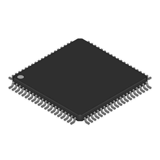


 工商网监
湘ICP备2023018690号
工商网监
湘ICP备2023018690号

