Low Skew CMOS PLL Clock Drivers
The MC88915 Clock Driver utilizes phase-locked loop technology to lock its low skew
outputs' frequency and phase onto an input reference clock. It is designed to provide clock
distribution for high performance PC's and workstations.
The PLL allows the high current, low skew outputs to lock onto a single clock input and
distribute it to multiple components on a board. The PLL also allows the MC88915 to
multiply a low frequency input clock and distribute it locally at a higher (2X) system
frequency. Multiple 88915's can lock onto a single reference clock, which is ideal for
applications when a central system clock must be distributed synchronously to multiple
boards (see Figure 9).
Five “Q” outputs (QO-Q4) are provided with less than 500 ps skew between their rising
edges. The Q5 output is inverted (180° phase shift) from the “Q” outputs. The 2X_Q output
runs at twice the “Q” output frequency, while the Q/2 runs at 1/2 the “Q” frequency.
The VCO is designed to run optimally between 20 MHz and the 2X_Q Fmax
specification. The wiring diagrams in Figure 5 detail the different feedback configurations
which create specific input/output frequency relationships. Possible frequency ratios of the
“Q” outputs to the SYNC input are 2:1, 1:1, and 1:2.
The FREQ_SEL pin provides one bit programmable divide-by in the feedback path of
the PLL. It selects between divide-by-1 and divide-by-2 of the VCO before its signal
reaches the internal clock distribution section of the chip (see the block diagram on page
2). In most applications FREQ_SEL should be held high (÷1). If a low frequency reference
clock input is used, holding FREQ_SEL low (÷2) will allow the VCO to run in its optimal
range (>20 MHz).
In normal phase-locked operation, the PLL_EN pin is held high. Pulling the PLL_EN pin
low disables the VCO and puts the 88915 in a static “test mode”. In this mode there is no
frequency limitation on the input clock, which is necessary for a low frequency board test
environment. The second SYNC input can be used as a test clock input to further simplify
board-level testing (see detailed description on page 11).
A lock indicator output (LOCK) will go high when the loop is in steady-state phase and
frequency lock. The LOCK output will go low if phase-lock is lost or when the PLL_EN pin
is low. Under certain conditions the lock output may remain low, even though the part is
phase-locked. Therefore, the LOCK output signal should not be used to drive any active
circuitry; it should be used for passive monitoring or evaluation purposes only.
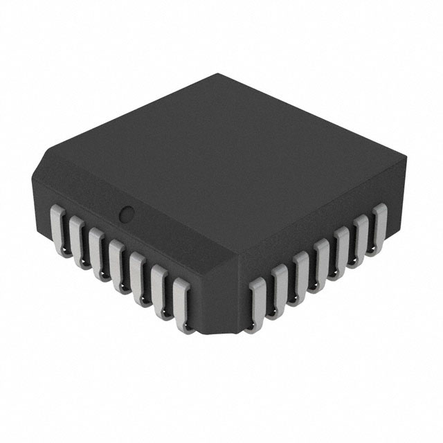
MC88915
MC88915
LOW SKEW CMOS PLL
CLOCK DRIVER
FN SUFFIX
28-LEAD PLCC PACKAGE
CASE 776-02
EI SUFFIX
28-LEAD PLCC PACKAGE
Pb-FREE PACKAGE
CASE 776-02
Features
•
•
•
•
•
•
•
•
Five outputs (Q0–Q4) with output-output skew < 500 ps, each being phase and frequency locked to the SYNC input
The phase variation from part-to-part between the SYNC and FEEDBACK inputs is less than 550 ps (derived from the tPD specification,
defining the part-to-part skew).
Input/output phase-locked frequency ratios of 1:2, 1:1, and 2:1 are available
Input frequency range from 5 MHz – 2X_Q fmax specification
Additional outputs available at 2X and +2 the system “Q” frequency. Also, a Q (180° phase shift) output available
All outputs have ±36 mA drive (equal high and low) at CMOS levels, and can drive either CMOS or TTL inputs. All inputs are
TTL-level compatible.
Test mode pin (PLL_EN) provided for low frequency testing. Two selectable CLOCK inputs for test or redundancy purposes.
28-lead Pb-free package available.
IDT™ / ICS™ CMOS PLL CLOCK DRIVERS
1
MC88915 REV 6 JULY 10, 2007
�MC88915
LOW SKEW CMOS PLL CLOCK DRIVERS
RST VCC Q5 GND Q4 VCC 2X_Q
4
3
2
1
28
27 26
FEEDBACK
5
25
Q/2
REF_SEL
6
24
GND
SYNC[0]
7
23
Q3
VCC(AN)
8
22
VCC
RC1
9
21
Q2
10
20
GND
11
19
LOCK
GND(AN)
SYNC[1]
12
13 14
15 16
17 18
FREQ_SEL GND Q0 VCC Q1 GND PLL_EN
Figure 1. Pinout: 28-Lead PLCC (Top View)
Table 1. Pin Summary
Pin Name
Number
I/O
SYNC[0]
1
Input
Reference clock input
SYNC[1]
1
Input
Reference clock input
REF_SEL
1
Input
Chooses reference between SYNC[0] and SYNC[1]
FREQ_SEL
1
Input
Selects Q output frequency
FEEDBACK
1
Input
Feedback input to phase detector
RC1
1
Input
Input for external RC network
Q(0–4)
5
Output
Clock output (locked to SYNC)
Q5
1
Output
Inverse of clock output
2x_Q
1
Output
2 x clock output (Q) frequency (synchronous)
Q/2
1
Output
Clock output (Q) frequency ÷ 2 (synchronous)
LOCK
1
Output
Indicates phase lock has been achieved (high when locked)
RST
1
Input
Asynchronous reset (active low)
PLL_EN
1
Input
Disables phase-lock for low frequency testing
VCC, GND
11
IDT™ / ICS™ CMOS PLL CLOCK DRIVERS
Function
Power and ground pins (note pins 8 and 10 are “quiet” supply pins
for internal logic only)
2
MC88915 REV 6 JULY 10, 2007
�MC88915
LOW SKEW CMOS PLL CLOCK DRIVERS
LOCK
FEEDBACK
SYNC (0)
0
SYNC (1)
1
M
U
X
PHASE/FREQ
DETECTOR
CHARGE PUMP/LOOP
FILTER
VOLTAGE
CONTROLLED
OSCILLATOR
EXTERNAL REC NETWORK
(RC1 PIN)
REF_SEL
0
PLL_EN
1
2x_Q
MUX
(÷1)
1
(÷2)
0
DIVIDE
BY TWO
M
U
X
D
Q
CP
Q
R
D
Q0
Q
Q1
Q
Q2
Q
Q3
Q
Q4
Q
Q5
Q
Q/2
CP
R
FREQ_SEL
RST
D
CP
R
D
CP
R
D
CP
R
D
CP
R
D
CP
R
Figure 2. MC88915 Block Diagram
IDT™ / ICS™ CMOS PLL CLOCK DRIVERS
3
MC88915 REV 6 JULY 10, 2007
�MC88915
LOW SKEW CMOS PLL CLOCK DRIVERS
Table 2. DC Electrical Characteristics (Voltages Referenced to GND)
TA = 0°C to +70°C, VCC = 5.0 V ± 5%
VCC
V
Target
Limit
Unit
4.75
2.0
V
5.25
2.0
4.75
0.8
5.25
0.8
4.75
4.01
IOH = –36 mA
5.25
4.51
Vin = VIH or VIL
4.75
0.44
IOH = 36 mA(1)
5.25
0.44
Maximum Input Leakage Current
VI = VCC or GND
5.25
± 1.0
µA
Maximum ICC/Input
VI = VCC – 2.1 V
5.25
1.5(2)
mA
VOLD = 1.0 V Maximum
5.25
88
mA
VOHD = 3.85 V Minimum
5.25
–88
mA
VI = VCC or GND
5.25
1.0
mA
Symbol
VIH
VIL
VOH
Parameter
Test Conditions
Minimum High-Level Input Voltage
Maximum Low-Level Input Voltage
Minimum High-Level Output Voltage
Vout = 0.1 V or VCC – 0.1 V
Vout = 0.1 V or VCC – 0.1 V
Vin = VIH or VIL
(1)
VOL
Iin
ICCT
IOLD
Maximum Low-Level Output Voltage
Minimum Dynamic Output
Current(3)
IOHD
ICC
Maximum Quiescent Supply Current (per Package)
V
V
V
1. IOL and IOH are 12 mA and -12 mA respectively for the LOCK output.
2. The PLL_EN input pin is not guaranteed to meet this specification.
3. Maximum test duration is 2.0ms, one output loaded at a time.
Table 3. Capacitance and Power Specifications
Symbol
Parameter
Typical Values
Unit
Conditions
CIN
Input Capacitance
4.5
pF
VCC = 5.0 V
CPD
Power Dissipation Capacitance
40
pF
VCC = 5.0 V
PD1
Power Dissipation @ 33 MHz with 50 Ω Thevenin Termination
15 mW/Output
mW
VCC = 5.0 V
mW
VCC = 5.0 V
120 mW/Device
PD2
Power Dissipation @ 33 MHz with 50 Ω Parallel Termination to GND
37.5 mW/Output
T = 25°C
300 mW/Device
T = 25°C
Table 4. SYNC Input Timing Requirements
Symbol
Parameter
Minimum
Maximum
Unit
tRISE/FALL
Maximum Rise and Fall times, SYNC Inputs from 0.8 to 2.0 V
—
3.0
ns
tCYCLE
Duty Cycle
Input Clock Period SYNC Inputs
Input Duty Cycle SYNC Inputs
FN55
FN70
36
28.5
200
(1)
ns
50% ± 25%
1. Information in Figure 5 and in Note 3. in the General AC Specification Notes describes this specification and its actual limits depending on
application.
Table 5. Frequency Specifications (TA = 0°C to +70 °C, VCC = 5.0 V ± 5%, CL = 5.0 pF)
Symbol
fmax(1)
Guaranteed Minimum
Parameter
Maximum Operating Frequency (2X_Q Output)
Maximum Operating Frequency (Q0–Q4, Q5 Output)
Unit
MC88915FN55
MC88915FN70
55
70
MHz
27.5
35
MHz
1. Maximum Operating Frequency is guaranteed with the part in a phase-locked condition, and all outputs loaded at 50 pF.
IDT™ / ICS™ CMOS PLL CLOCK DRIVERS
4
MC88915 REV 6 JULY 10, 2007
�MC88915
LOW SKEW CMOS PLL CLOCK DRIVERS
Table 6. AC Electrical Characteristics (TA =0° C to +70° C, VCC = 5.0V ±5%, CL = 50pF)
Symbol
Parameter
Min
Max
Unit
tRISE, tFALL
(Outputs)
Rise and Fall Times, all Outputs Into a 50 pF, 500 Ω Load (Between
0.2 VCC and 0.8 VCC)
1.0
2.5
ns
tRISE, tFALL(1)
(2X_Q Output)
Rise and Fall Time, 2X_Q Output Into a 20 pF Load With Termination
specified in note 2 (Between 0.8 V and 2.0 V)
0.5
1.6
ns
tPulse Width(1)
(Q0,Q1,Q3,Q4,
Q5,Q/2)
Output Pulse Width (Q0, Q1, Q3, Q4, Q5, Q/2 @VCC/2)
0.5tCYCLE - 0.5
0.5tCYCLE + 0.5
tPulse Width(1)
(Q2 only)
ns
tCYCLE = 1/Freq. at which the “Q”
Outputs are running
Output Pulse Width (Q2 Output @ VCC/2)
0.5tCYCLE - 0.6
0.5tCYCLE + 0.6
ns
tPulse Width(1)
(2X_Q Output)
Output Pulse Width (2X_Q Output @ 1.5 V) (See General AC
Specification note 2)
0.5tCYCLE - 0.5
0.5tCYCLE + 0.5
ns
tPulse Width(1)
(2X_Q Output)
Output Pulse Width (2X_Q Output @ VCC/2)
0.5tCYCLE - 1.0
0.5tCYCLE + 1.0
ns
tPD(1)
(Sync-Feedback)
SYNC input to feedback delay
(meas. @ SYNC0 or 1 and FEEDBACK input pins)
(See General AC Specification Note 4. and Figure 4 for explanation)
(470 kΩ From RC1 to An. VCC)
-1.05
-0.50
ns
(470 kΩ From RC1 to An. GND)
+1.25
+3.25
Output-to-Output Skew Between Outputs Q0 - Q4, Q/2
(Rising Edges Only)
—
500
ps
Output-to-Output Skew Between Outputs Q0 - Q4
(Falling Edges Only)
—
750
ps
tSKEWall (1), (2)
Output-to-Output Skew Between Outputs 2X_Q, Q/2, Q0 - Q4
Rising, Q5 Falling
—
750
ps
tLOCK
Time Required to acquire (3) Phase-Lock from time SYNC Input
Signal is Received.
1
10
ms
1.5
13.5
ns
tSKEWr(2)
(Rising)
tSKEWf(1), (2)
(Falling)
tPHL
(Reset - Q)
Propagation Delay, RST to Any Output (High-Low)
1. These specifications are not tested, they are guaranteed by statistical characterization. See General AC Specification note 1.
2. Under equally loaded conditions, CL ≤ 50 pF (±2 pF), and at a fixed temperature and voltage.
3. With VCC fully powered-on and an output properly connected to the FEEDBACK pin. tLOCK, Max. is with C1 = 0.1µF, tLOCK Min. is with
C1 = 0.01µF.
Table 7. Reset Timing Requirements(1)
Symbol
Parameter
Minimum
Unit
tREC, RST
to SYNC
Reset Recovery Time rising RST edge to falling SYNC edge
9.0
ns
Minimum Pulse Width, RST input LOW
5.0
ns
tW, RST
LOW
1. These reset specs are valid only when PLL_EN is LOW and the part is in Test mode (not in phase-lock)
IDT™ / ICS™ CMOS PLL CLOCK DRIVERS
5
MC88915 REV 6 JULY 10, 2007
�MC88915
LOW SKEW CMOS PLL CLOCK DRIVERS
GENERAL AC SPECIFICATION NOTES
1. Statistical characterization techniques were used to
guarantee those specifications which cannot be
measured on the ATE. MC88915 units were fabricated
with key transistor properties intentionally varied to
create a 14-cell designed experimental matrix. IC
performance was characterized over a range of
transistor properties (represented by the 14 cells) in
excess of the expected process variation of the wafer
fabrication area. In this way all units passing the ATE
test will meet or exceed the non-tested specifications
limits.
2. These two specs (tRISE/FALL and tPULSE Width 2X_Q
output) guarantee the MC88915 meets the 25 MHz
MC68040 P-Clock input specification (at 50 MHz). For
88915
2X_Q OUTPUT
RS
3.
these two specs to be guaranteed by Freescale
Semiconductor, the termination scheme shown below in
Figure 3 must be used.
The wiring diagrams and explanations in Figure 7
demonstrate the input and output frequency
relationships for three possible feedback configurations.
The allowable SYNC input range for each case is also
indicated. There are two allowable SYNC frequency
ranges, depending whether FREQ_SEL is high or low.
Although not shown, it is possible to feed back the Q5
output, thus creating a 180° phase shift between the
SYNC input and the “Q” outputs. Table 8 below
summarizes the allowable SYNC frequency range for
each possible configuration.
ZO (CLOCK TRACE)
RS = ZO – 7 Ω
68040
P-CLOCK INPUT
RP
RP = 1.5 ZO
Figure 3. MC68040 P-Clock Input Termination Scheme
Table 8. Allowable SYNC Input Frequency Ranges for Different Feedback Configurations
FREQ_SEL
Level
4.
Feedback
Output
Allowable SYNC Input
Frequency Range (MHz)
Corresponding VCO
Frequency Range
Phase Relationships
of the “Q” Outputs
to Rising SYNC Edge
HIGH
Q/2
5 to (2X_Q FMAX Spec)/4
20 to (2X_Q FMAX Spec)
HIGH
Any “Q” (Q0–Q4)
10 to (2X_Q FMAX Spec)/2
20 to (2X_Q FMAX Spec)
0°
0°
HIGH
Q5
10 to (2X_Q FMAX Spec)/2
20 to (2X_Q FMAX Spec)
180°
HIGH
2X_Q
20 to (2X_Q FMAX Spec)
20 to (2X_Q FMAX Spec)
0°
0°
LOW
Q/2
2.5 to (2X_Q FMAX Spec)/8
20 to (2X_Q FMAX Spec)
LOW
Any “Q” (Q0–Q4)
5 to (2X_Q FMAX Spec)/4
20 to (2X_Q FMAX Spec)
0°
LOW
Q5
5 to (2X_Q FMAX Spec)/4
20 to (2X_Q FMAX Spec)
180°
LOW
2X_Q
10 to (2X_Q FMAX Spec)/2
20 to (2X_Q FMAX Spec)
0°
A 1 MΩ resistor tied to either Analog VCC or Analog
GND, depicted in Figure 4, is required to ensure no jitter
is present on the MC88915 outputs. This technique
causes a phase offset between the SYNC input and the
output connected to the FEEDBACK input, measured at
the input pins. The tPD spec describes how this offset
varies with process, temperature, and voltage. The
specs were determined by measuring the phase
IDT™ / ICS™ CMOS PLL CLOCK DRIVERS
relationship for the 14 lots described in Note 1 while the
part was in phase-locked operation. The actual
measurements were made with a 10 MHz SYNC input
(1.0 ns edge rate from 0.8 V – 2.0 V) with the Q/2 output
fed back. The phase measurements were made at
1.5 V. The Q/2 output was terminated at the
FEEDBACK input with 100 Ω to VCC and 100 Ω to
ground.
6
MC88915 REV 6 JULY 10, 2007
�MC88915
LOW SKEW CMOS PLL CLOCK DRIVERS
RC1
EXTERNAL LOOP FILTER
ANALOG VCC
330 Ω
0.1 µF
C1
RC1
1 MΩ
or
470 kΩ
Reference
Resistor
R2
1 MΩ
or
470 kΩ
Reference
Resistor
330 Ω
R2
0.1 µF
C1
ANALOG GND
ANALOG GND
With the 470 kΩ resistor tied in this fashion, the tPD
specification measured at the input pins is:
With the 470 kΩ resistor tied in this fashion, the tPD
specification measured at the input pins is:
tPD = 2.25 ns ± 1.0 ns
tPD = –0.775 ns ± 0.275 ns
3.0 V
SYNC INPUT
2.25 ns OFFSET
SYNC INPUT
–0.775 ns OFFSET
5.0 V
5.0 V
FEEDBACK OUTPUT
FEEDBACK OUTPUT
3.0 V
Figure 4. Depiction of the Fixed SYNC to Feedback Offset (tPD)
Which is Present When a 470 kΩ Resistor is Tied to VCC or Ground
5.
6.
The tSKEWr specification guarantees the rising edges of
outputs Q/2, Q0, Q1, Q2, Q3, and Q4 will always fall
within a 500 ps window within one part. However, if the
relative position of each output within this window is not
specified, the 500 ps window must be added to each
side of the tPD specification limits to calculate the total
part-to-part skew. For this reason, the absolute
distribution of these outputs are provided in Table 9.
When taking the skew data, Q0 was used as a
reference, so all measurements are relative to this
output. The information in Table 9 is derived from
measurements taken from the 14 process lots described
in Note 1, over the temperature and voltage range.
Table 9. Relative Positions of Outputs Q/2, Q0–Q4,
2X_Q Within the 500 ps tSKEWr Spec Window
Output
Calculation of Total Output-to-Skew Between
Multiple Parts (Part-to-Part Skew)
By combining the tPD specification and the information in
Note 5, the worst case output-to-output skew between
multiple 88915s connected in parallel can be calculated.
This calculation assumes all parts have a common
SYNC input clock with equal delay of input signal to each
part. This skew value is valid at the 88915 output pins
only (equally loaded), it does not include PCB trace delays due to varying loads.
+ (ps)
Q0
0
0
Q1
–72
40
Q2
–44
276
Q3
–40
255
Q4
–274
–34
Q/2
–16
250
2X_Q
–633
–35
0.32 ns] = –1.37 ns is the lower tPD limit, and [–0.5 ns +
0.32 ns] = –0.18 ns is the upper limit. Therefore, the
worst case skew of output Q2 between any number of
parts is |(–1.37) – (–0.18)| = 1.19 ns. Q2 has the worst
case skew distribution of any output, so 1.2 ns is the absolute worst case output-to-output skew between multiple parts.
7.
With a 1.0 MΩ resistor tied to analog VCC as shown in
Note 4, the tPD spec. limits between SYNC and the Q/2
output (connected to the FEEDBACK pin) are –1.05 ns
and –0.5 ns. To calculate the skew of any given output
between two or more parts, the absolute value of the distribution of the output given in Table 9 must be subtracted and added to the lower and upper tPD spec limits
respectively. For output Q2, [276 – (–44)] = 320 ps is the
absolute value of the distribution. Therefore, [–1.05 ns –
IDT™ / ICS™ CMOS PLL CLOCK DRIVERS
– (ps)
Note 4 explains that the tPD specification was measured
and is guaranteed for the configuration of the Q/2 output
connected to the FEEDBACK pin and the SYNC input
running at 10 MHz. The fixed offset (tPD) as described
above has some dependence on the input frequency
and at what frequency the VCO is running. The graphs
of Figure 5 demonstrate this dependence.
The data presented in Figure 5 is from devices representing process extremes, and the measurements were
also taken at the voltage extremes (VCC = 5.25 V and
4.75 V). Therefore, the data in Figure 5 is a realistic representation of the variation of tPD.
7
MC88915 REV 6 JULY 10, 2007
�MC88915
LOW SKEW CMOS PLL CLOCK DRIVERS
–0.5
tPD SYNC TO FEEDBACK (ns)
tPD SYNC TO FEEDBACK (ns)
–0.50
–0.75
–1.00
–1.25
–1.50
2.5
5.0
7.5
10.0
12.5
15.0
SYNC INPUT FREQUENCY (MHz)
–1.0
–1.5
–2.0
2.5
17.5
Figure 5a
tPD versus Frequency Variation for Q/2 Output Fed
Back, Including Process and Voltage Variation @ 25°C
(with 1.0 MΩ Resistor Tied to Analog VCC)
tPD versus Frequency Variation for Q4 Output Fed
Back, Including Process and Voltage Variation @ 25°C
(with 1.0 MΩ Resistor Tied to Analog VCC)
3.5
3.0
tPD SYNC TO FEEDBACK (ns)
tPD SYNC TO FEEDBACK (ns)
12.5
17.5
27.5
25.0
10.0
15.0
20.0
22.5
SYNC INPUT FREQUENCY (MHz)
Figure 5b
3.5
2.5
2.0
1.5
1.0
0.5
7.5
5.0
2.5
5.0
7.5
10.0
12.5
15.0
SYNC INPUT FREQUENCY (MHz)
3.0
2.5
2.0
1.5
1.0
0.5
17.5
Figure 5c
0
5
10
15
20
SYNC INPUT FREQUENCY (MHz)
25
Figure 5d
tPD versus Frequency Variation for Q/2 Output Fed
Back, Including Process and Voltage Variation @ 25°C
(with 1.0 MΩ Resistor Tied to Analog GND)
tPD versus Frequency Variation for Q4 Output Fed
Back, Including Process and Voltage Variation @ 25°C
(with 1.0 MΩ Resistor Tied to Analog GND)
Figure 5. Graphs
IDT™ / ICS™ CMOS PLL CLOCK DRIVERS
8
MC88915 REV 6 JULY 10, 2007
�MC88915
LOW SKEW CMOS PLL CLOCK DRIVERS
SYNC INPUT
(SYNC[1] OR
SYNC[0])
tCYCLE SYNC INPUT
tPD
FEEDBACK
INPUT
Q/2 OUTPUT
tSKEWr
tSKEWALL
tSKEWf
tSKEWr
tSKEWf
Q0–Q4
OUTPUTS
tCYCLE "Q" OUTPUTS
Q5 OUTPUT
2X_Q OUTPUT
Figure 6. Output/Input Switching Waveforms and Timing Diagrams
(These waveforms represent the hook-up configuration of Figure 7a.)
TIMING NOTES:
1. The MC88915 aligns rising edges of the FEEDBACK
input and SYNC input; therefore, the SYNC input does
not require a 50% duty cycle.
2. All skew specs are measured between the VCC/2
crossing point of the appropriate output edges. All
skews are specified as “windows,” not as a ± deviation
around a center point.
IDT™ / ICS™ CMOS PLL CLOCK DRIVERS
3.
9
If a “Q” output is connected to the FEEDBACK input
(this situation is not shown), the “Q” output frequency
would match the SYNC input frequency, the 2X_Q
output would run at twice the SYNC frequency, and the
Q/2 output would run at half the SYNC frequency.
MC88915 REV 6 JULY 10, 2007
�MC88915
LOW SKEW CMOS PLL CLOCK DRIVERS
12.5 MHz FEEDBACK SIGNAL
HIGH
RST
Q5
FEEDBACK
LOW
CRYSTAL 12.5 MHz INPUT
OSCILLATOR
REF_SEL
Q4
2X_Q
Q/2
MC88915
SYNC[0]
Q3
ANALOG VCC
EXTERNAL
LOOP
FILTER
50 MHz SIGNAL
25 MHz
“Q” CLOCK
OUTPUTS
Q2
RC1
ANALOG GND
FQ_SEL
Q0
Q1 PLL_EN
HIGH
1:2 Input to “Q” Output Frequency Relationship
In this application, the Q/2 output is connected to
the FEEDBACK input. The internal PLL will line up
the positive edges of Q/2 and SYNC, thus the Q/2
frequency will equal the SYNC frequency. The “Q”
outputs (Q0–Q4, Q5) will always run at 2X the Q/2
frequency, and the 2X_Q output will run at 4X the
Q/2 frequency.
Allowable Input Frequency Range:
5 MHz to (2X_Q FMAX Spec)/4 (for FREQ_SEL HIGH)
2.5 MHz to (2X_Q FMAX Spec)/8 (for FREQ_SEL LOW)
HIGH
Figure 7a. Wiring Diagram and Frequency Relationships with Q/2 Output Feedback
25 MHz FEEDBACK SIGNAL
HIGH
RST
Q5
FEEDBACK
LOW
CRYSTAL 25 MHz INPUT
OSCILLATOR
REF_SEL
Q4
50 MHz SIGNAL
2X_Q
Q/2
1:1 Input to “Q” Output Frequency Relationship
In this application, the Q4 output is connected to
the FEEDBACK input. The internal PLL will line up
the positive edges of Q4 and SYNC, thus the Q4
frequency (and the rest of the “Q” outputs) will
equal the SYNC frequency. The Q/2 output will
always rn at 1/2 the “Q” frequency, and the 2X_Q
output will run at 2X the “Q” frequency.
12.5 MHz
SIGNAL
MC88915
SYNC[0]
Q3
ANALOG VCC
EXTERNAL
LOOP
FILTER
Q2
RC1
ANALOG GND
FQ_SEL
Q0
Q1 PLL_EN
HIGH
25 MHz
“Q” CLOCK
OUTPUTS
Allowable Input Frequency Range:
10 MHz to (2X_Q FMAX Spec)/2 (for FREQ_SEL HIGH)
5 MHz to (2X_Q FMAX Spec)/4 (for FREQ_SEL LOW)
HIGH
Figure 7b. Wiring Diagram and Frequency Relationships with Q4 Output Feedback
50 MHz FEEDBACK SIGNAL
HIGH
RST
Q5
FEEDBACK
LOW
CRYSTAL 50 MHz INPUT
OSCILLATOR
EXTERNAL
LOOP
FILTER
REF_SEL
Q4
2:1 Input to “Q” Output Frequency Relationship
2X_Q
Q/2
12.5 MHz
SIGNAL
MC88915
SYNC[0]
Q3
ANALOG VCC
Q2
RC1
ANALOG GND
FQ_SEL
In this application, the 2X_Q output is connected to
the FEEDBACK input. The internal PLL will line up
the positive edges of 2X_Q and SYNC, thus the
2X_Q frequency will equal the SYNC frequency.
The Q/2 output will always run at 1/4 the 2X_Q
frequency, and the “Q” outputs will run at 1/2 the
2X_Q frequency.
Q0
HIGH
25 MHz
“Q” CLOCK Allowable Input Frequency Range:
OUTPUTS
20 MHz to (2X_Q FMAX Spec) (for FREQ_SEL HIGH)
10 MHz to (2X_Q FMAX Spec)/2 (for FREQ_SEL LOW)
Q1 PLL_EN
HIGH
Figure 7c. Wiring Diagram and Frequency Relationships with 2X_Q Output Feedback
Figure 7. Wiring Diagrams
IDT™ / ICS™ CMOS PLL CLOCK DRIVERS
10
MC88915 REV 6 JULY 10, 2007
�MC88915
LOW SKEW CMOS PLL CLOCK DRIVERS
BOARD VCC
47 Ω
10 µF LOW
FREQUENCY
BYPASS
0.1 µF HIGH
FREQUENCY
BYPASS
1 MΩ
OR
470 kΩ
330 Ω
0.1 µF (LOOP
FILTER CAP)
8
ANALOG VCC
9
RC1
10
ANALOG GND
ANALOG LOOP FILTER/VCO
SECTION OF THE MC88915
28-PIN PLCC PACKAGE (NOT
DRAWN TO SCALE)
47 Ω
BOARD GND
NOTE: A separate analog power supply is not necessary and
should not be used. Following these prescribed guidelines
is all that is necessary to use the MC88915 in a normal
digital environment.
Figure 8. Recommended Loop Filter and Analog Isolation Scheme for the MC88915
NOTES CONCERNING LOOP FILTER AND BOARD LAYOUT ISSUES
digital VCC supply. The purpose of the bypass
1. Figure 8 shows a loop filter and analog isolation
scheme which will be effective in most applications. The
filtering scheme shown in Figure 8 is to give the
following guidelines should be followed to ensure stable
88915 additional protection from the power supply
and jitter-free operation:
and ground plane transients potentially occurring in
a high frequency, high speed digital system.
a. All loop filter and analog isolation components
should be tied as close to the package as possible.
c. There are no special requirements set forth for the
Stray current passing through the parasitics of long
loop filter resistors (1 MΩ or 470 KΩ and 330 Ω).
traces can cause undesirable voltage transients at
The loop filter capacitor (0.1 µF) can be a ceramic
the RC1 pin.
chip capacitor, the same as a standard bypass
capacitor.
b. The 47 Ω resistors, the 10 µF low frequency bypass
capacitor, and the 0.1 µF high frequency bypass
d. The 1 MΩ or 470 KΩ reference resistor injects
capacitor form a wide bandwidth filter minimizing
current into the internal charge pump of the PLL,
the 88915’s sensitivity to voltage transients from
causing a fixed offset between the outputs and the
the system digital VCC supply and ground planes.
SYNC input. This also prevents excessive jitter
This filter will typically ensure a 100 mV step
caused by inherent PLL dead-band. If the VCO
deviation on the digital VCC supply, causing no
(2X_Q output) is running above 40 MHz, the 470
KΩ resistor provides the correct amount of current
more than a 100 ps phase deviation o the 88915
injection into the charge pump (2–3 µA). if the VCO
outputs. A 250 mV step deviation on VCC using the
is
running below 40 MHz, a 1.0 MΩ reference
recommended filter values should cause no more
resistor should be used (instead of 470 KΩ).
than 250 ps phase deviation; if a 25 µF bypass
2. In addition to the bypass capacitors used in the analog
capacitor is used (instead of 10 µF) a 250 mV VCC
filter of Figure 8, there should be a 0.1 µF bypass
step should cause no more than a 100 ps phase
capacitor between each of the other (digital) four VCC
deviation.
pins and the board ground plane. This will reduce output
If good bypass techniques are used on a board
switching noise caused by the 88915 outputs, in
design near components potentially causing digital
addition to reducing potential for noise in the “analog”
VCC and ground noise, the above described VCC
section of the chip. These bypass capacitors should
step deviations should not occur at the 88915’s
also be tied as close to the 88915 package as possible.
IDT™ / ICS™ CMOS PLL CLOCK DRIVERS
11
MC88915 REV 6 JULY 10, 2007
�MC88915
LOW SKEW CMOS PLL CLOCK DRIVERS
CLOCK
@f
MC88915
PLL
2f
SYSTEM
CLOCK
SOURCE
MC88915
PLL
2f
DISTRIBUTE
CLOCK @ f
CMMU
CMMU
CPU
CMMU
CMMU
CMMU
CMMU
CMMU
CPU
CMMU
CMMU
CMMU
CPU
CARD
CPU
CARD
CLOCK @ 2f
AT POINT OF USE
MC88915T
PLL
2f
MEMORY
CARDS
MEMORY
CONTROL
CLOCK @ 2f
AT POINT OF USE
Figure 9. Representation of a Potential Multi-Processing Application Utilizing the MC88915
for Frequency Multiplication and Low Board-to-Board Skew
MC88915 SYSTEM LEVEL TESTING FUNCTIONALITY
When the PLL_EN pin is low, the VCO is disabled and the
88915 is in low frequency “test mode”. In test mode (with
FREQ_SEL high), the 2X_Q output is inverted from the
selected SYNC input, and the “Q” outputs are divide-by-2
(negative edge triggered) of the SYNC input, and the Q/2
output is divide-by-4. With FREQ_SEL low the 2X_Q output
is divide-by-2 of the SYNC, the “Q” outputs divide-by-4, and
the Q/2 output divide-by-8. These relationships can be seen
on the block diagram. A recommended test configuration
IDT™ / ICS™ CMOS PLL CLOCK DRIVERS
would be to use SYNC0 as the test clock input, and tie
PLL_EN and REF_SEL together and connect them to the test
select logic. When these inputs are low, the 88915 is in test
mode and the SYNC0 input is selected.
This functionality is needed since most board-level testers
run at 1 MHz or below, and the 88915 cannot lock onto that
low of an input frequency. In the test mode described above,
any frequency test signal can be used.
12
MC88915 REV 6 JULY 10, 2007
�MC88915
LOW SKEW CMOS PLL CLOCK DRIVERS
PACKAGE DIMENSIONS
PACKAGE DIMENSIONS
CASE 776-02
ISSUE D
PLCC PLASTIC PACKAGE
IDT™ / ICS™ CMOS PLL CLOCK DRIVERS
13
MC88915 REV 6 JULY 10, 2007
�MC88915
LOW SKEW CMOS PLL CLOCK DRIVERS
Innovate with IDT and accelerate your future networks. Contact:
www.IDT.com
For Sales
For Tech Support
800-345-7015
408-284-8200
Fax: 408-284-2775
netcom@idt.com
480-763-2056
Corporate Headquarters
Asia Pacific and Japan
Europe
Integrated Device Technology, Inc.
6024 Silver Creek Valley Road
San Jose, CA 95138
United States
800 345 7015
+408 284 8200 (outside U.S.)
Integrated Device Technology
Singapore (1997) Pte. Ltd.
Reg. No. 199707558G
435 Orchard Road
#20-03 Wisma Atria
Singapore 238877
+65 6 887 5505
IDT Europe, Limited
321 Kingston Road
Leatherhead, Surrey
KT22 7TU
England
+44 (0) 1372 363 339
Fax: +44 (0) 1372 378851
© 2007 Integrated Device Technology, Inc. All rights reserved. Product specifications subject to change without notice. IDT and the IDT logo are trademarks of Integrated Device
Technology, Inc. Accelerated Thinking is a service mark of Integrated Device Technology, Inc. All other brands, product names and marks are or may be trademarks or registered
trademarks used to identify products or services of their respective owners.
Printed in USA
�