DATASHEET
MK3200
32.768 KHZ CLOCK OSCILLATOR
Description
Features
The MK3200 is IDT’s lowest cost, low power clock oscillator
that generates a low power 32.768 kHz output from an
inexpensive 32.768 kHz crystal. This part includes a power
down pin and allows you to tri-state the output clock for
in-circuit testing.
•
•
•
•
•
•
•
IDT manufactures the largest variety of clock synthesizers
for all applications. If more clock outputs are needed,
including MHz frequencies, see the MK32xx family of parts.
Consult IDT to eliminate VCXOs, crystals and oscillators
from your board.
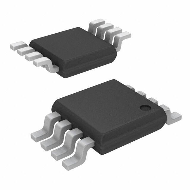
Packaged in 8-pin SOIC or 8-pin MSOP (3.00 mm body)
Pb (lead) free package
Operates from 2.5 V to 5 V
Consumes only 3.5 µA in normal operation
Accepts an inexpensive 32.768 kHz crystal input
Offers power down mode
Includes an Output Enable pin to tri-state the output for
in-circuit testing
• Advanced, low power, sub-micron CMOS process
• For other 32.768 kHz-based clocks with MHz outputs,
please consult IDT
• Industrial temperature version available
Block Diagram
VDD
Power Down
X1
Crystal
Oscillator
32.768 kHz
Crystal
32.768 kHz
Clock
X2
GND
IDT® 32.768 KHZ CLOCK OSCILLATOR
OE
1
MK3200
REV H 073012
�MK3200
32.768 KHZ CLOCK OSCILLATOR
32 KHZ OSCILLATOR
Pin Assignment
Power Down Select Table
X1
1
8
X2
VDD
2
7
GND
GND
3
6
PD
32. 768k
4
5
OE
PD
0
1
32.768k
On
Low
Oscillator
On
Off
Output Enable Select Table
8-pin (150 mil) SOIC or
8-pin MSOP (3.00 mm body)
OE
0
1
32.768k
Tri state (Hi-Z)
On
Oscillator
On
On
0 = connect directly to GND.
1 = connect directly to VDD.
Pin Descriptions
Pin
Number
1
2
3
4
5
6
7
8
Pin
Name
X1
VDD
GND
32.768k
OE
PD
GND
X2
IDT® 32.768 KHZ CLOCK OSCILLATOR
Pin
Type
Input
Power
Power
Input
Output
Input
Input
Output
Pin Description
Crystal connection. Connect to a 32.768 kHz crystal.
Connect to +3.3 V.
Connect to ground.
32.768 kHz clock output.
Output Enable.
Power down pin. Turns off entire chip when high.
Connect to ground.
Crystal connection. Connect to a 32.768 kHz crystal.
2
MK3200
REV H 073012
�MK3200
32.768 KHZ CLOCK OSCILLATOR
32 KHZ OSCILLATOR
External Components
Series Termination Resistor
Clock output traces over one inch should use series
termination. To series terminate a 50Ω trace (a commonly
used trace impedance), place a 33Ω resistor in series with
the clock line, as close to the clock output pin as possible.
The nominal impedance of the clock output is 20Ω.
Decoupling Capacitor
As with any high-performance mixed-signal IC, the MK3200
must be isolated from system power supply noise to perform
optimally.
A decoupling capacitor of 0.01µF must be connected
between VDD and the PCB ground plane.
PCB Layout Recommendations
For optimum device performance and lowest output phase
noise, the following guidelines should be observed.
1) The 0.01µF decoupling capacitor should be mounted on
the component side of the board as close to the VDD pin as
possible. No vias should be used between the decoupling
capacitor and VDD pin. The PCB trace to VDD pin should
be kept as short as possible, as should the PCB trace to the
ground via. Distance of the ferrite bead and bulk decoupling
from the device is less critical.
2) To minimize EMI, the 33Ω series termination resistor (if
needed) should be placed close to the clock output.
3) An optimum layout is one with all components on the
same side of the board, minimizing vias through other signal
layers. Other signal traces should be routed away from the
MK3200. This includes signal traces just underneath the
device, or on layers adjacent to the ground plane layer used
by the device.
4) The input crystal must be connected as close to the chip
as possible. The input crystal should be a parallel mode
crystal with a 12 pF load capacitance.
IDT® 32.768 KHZ CLOCK OSCILLATOR
3
MK3200
REV H 073012
�MK3200
32.768 KHZ CLOCK OSCILLATOR
32 KHZ OSCILLATOR
Absolute Maximum Ratings
Stresses above the ratings listed below can cause permanent damage to the MK3200. These ratings, which are
standard values for IDT commercially rated parts, are stress ratings only. Functional operation of the device at these
or any other conditions above those indicated in the operational sections of the specifications is not implied.
Exposure to absolute maximum rating conditions for extended periods can affect product reliability. Electrical
parameters are guaranteed only over the recommended operating temperature range.
Parameter
Condition
Min.
Supply Voltage, VDD
Referenced to GND
Inputs
Referenced to GND
Clock Outputs
Referenced to GND
Storage Temperature
Soldering Temperature
Typ.
Max.
Units
7
V
-0.5
VDD+ 0.5
V
-0.5
VDD+ 0.5
V
-65
150
°C
260
°C
125
°C
Max 10 seconds
Junction Temperature
Recommended Operation Conditions
Parameter
Min.
Ambient Operating Temperature
Typ.
Max.
Units
+85
°C
+3.45
V
-40
Power Supply Voltage (measured in respect to GND)
+3.15
+3.3
DC Electrical Characteristics
Unless stated otherwise, VDD = 3.3 V ±5%, Ambient Temperature -40 to +85° C
Parameter
Symbol
Conditions
Min.
Typ.
Units
5.250
V
Operating Voltage
VDD
Supply Current
IDD
No load, OE=1
3.5
μA
3.5
Output High Voltage
(CMOS level)
VOH
PD = 0
IOH = -1.5 mA
VDD-0.4
μA
V
Output High Voltage
VOH
IOH = -3 mA
2.4
V
Output Low Voltage
VOL
IOL = 3mA
Short Circuit Current
IOS
IDT® 32.768 KHZ CLOCK OSCILLATOR
2.375
Max.
0.4
±6
4
V
mA
MK3200
REV H 073012
�MK3200
32.768 KHZ CLOCK OSCILLATOR
32 KHZ OSCILLATOR
AC Electrical Characteristics
Unless stated otherwise, VDD = 3.3 V ±5%, Ambient Temperature -40 to +85° C
Parameter
Symbol
Input Frequency
FIN
Output Rise Time
tOR
Output Fall Time
tOF
Duty Cycle
Conditions
Min.
Typ.
Max. Units
32.768
kHz
20% to 80%, Note 1
8
ns
80% to 20%, Note 1
8
ns
at VDD/2
40
50
60
%
0
±30
ppm
Input Crystal Accuracy
Thermal Characteristics (8SOIC)
Parameter
Symbol
Thermal Resistance Junction to
Ambient
Conditions
Min.
Max. Units
θ JA
Still air
135
° C/W
θ JA
1 m/s air flow
93
° C/W
θ JA
3 m/s air flow
78
° C/W
60
° C/W
θ JC
Thermal Resistance Junction to Case
Typ.
Thermal Characteristics (8MSOP)
Parameter
Symbol
Thermal Resistance Junction to
Ambient
θJA
Thermal Resistance Junction to Case
θJC
IDT® 32.768 KHZ CLOCK OSCILLATOR
Conditions
Still air
5
Min.
Typ.
Max. Units
95
° C/W
48
° C/W
MK3200
REV H 073012
�MK3200
32.768 KHZ CLOCK OSCILLATOR
32 KHZ OSCILLATOR
Package Outline and Package Dimensions (8-pin MSOP, 3.00 mm Body)
Package dimensions are kept current with JEDEC Publication No. 95
Millimeters
8
Symbol
E1
A
A1
A2
b
C
D
E
E1
e
L
α
aaa
E
IN D E X
AREA
1
2
D
Min
Max
-1.10
0
0.15
0.79
0.97
0.22
0.38
0.08
0.23
3.00 BASIC
4.90 BASIC
3.00 BASIC
0.65 Basic
0.40
0.80
0°
8°
0.10
Inches*
Min
Max
-0.043
0
0.006
0.031
0.038
0.008
0.015
0.003
0.009
0.118 BASIC
0.193 BASIC
0.118 BASIC
0.0256 Basic
0.016
0.032
0°
8°
0.004
*For reference only. Controlling dimensions in mm.
A
2
A
A
1
c
-C e
b
S E A T IN G
P LA N E
L
aaa
IDT® 32.768 KHZ CLOCK OSCILLATOR
C
6
MK3200
REV H 073012
�MK3200
32.768 KHZ CLOCK OSCILLATOR
32 KHZ OSCILLATOR
Package Outline and Package Dimensions (8-pin SOIC, 150 Mil. Body)
Package dimensions are kept current with JEDEC Publication No. 95
Millimeters
8
Symbol
E
Min
A
A1
B
C
D
E
e
H
h
L
H
INDEX
AREA
1 2
D
Max
Min
1.35
1.75
0.10
0.25
0.33
0.51
0.19
0.25
4.80
5.00
3.80
4.00
1.27 BASIC
5.80
6.20
0.25
0.50
0.40
1.27
α
A
Inches
0°
Max
.0532
.0688
.0040
.0098
.013
.020
.0075
.0098
.1890
.1968
.1497
.1574
0.050 BASIC
.2284
.2440
.010
.020
.0
.050
8°
0°
8°
h x 45
A1
C
-Ce
B
SEATING
PLANE
L
.10 (.004)
C
Ordering Information
Part / Order Number
Marking
Shipping Packaging
Package
Temperature
MK3200SLF
MK3200SLFTR
MK3200SILF
MK3200SILFTR
MK3200GLF
MK3200GLFT
MK3200SL
MK3200SL
MK3200IL
MK3200IL
3200GL
3200GL
Tubes
Tape and Reel
Tubes
Tape and Reel
Tubes
Tape and Reel
8-pin SOIC
8-pin SOIC
8-pin SOIC
8-pin SOIC
8-pin MSOP
8-pin MSOP
0 to +70° C
0 to +70° C
-40 to +85° C
-40 to +85° C
0 to +70° C
0 to +70° C
While the information presented herein has been checked for both accuracy and reliability, Integrated Device Technology (IDT) assumes
no responsibility for either its use or for the infringement of any patents or other rights of third parties, which would result from its use. No
other circuits, patents, or licenses are implied. This product is intended for use in normal commercial applications. Any other applications
such as those requiring extended temperature range, high reliability, or other extraordinary environmental requirements are not
recommended without additional processing by IDT. IDT reserves the right to change any circuitry or specifications without notice. IDT
does not authorize or warrant any IDT product for use in life support devices or critical medical instruments.
IDT® 32.768 KHZ CLOCK OSCILLATOR
7
MK3200
REV H 073012
�MK3200
32.768 KHZ CLOCK OSCILLATOR
32 KHZ OSCILLATOR
Innovate with IDT and accelerate your future networks. Contact:
www.IDT.com
For Sales
For Tech Support
800-345-7015
408-284-8200
Fax: 408-284-2775
www.idt.com/go/clockhelp
Corporate Headquarters
Integrated Device Technology, Inc.
www.idt.com
© 2012 Integrated Device Technology, Inc. All rights reserved. Product specifications subject to change without notice. IDT and the IDT logo are trademarks of Integrated Device
Technology, Inc. Accelerated Thinking is a service mark of Integrated Device Technology, Inc. All other brands, product names and marks are or may be trademarks or registered
trademarks used to identify products or services of their respective owners.
Printed in USA
�IMPORTANT NOTICE AND DISCLAIMER
RENESAS ELECTRONICS CORPORATION AND ITS SUBSIDIARIES (“RENESAS”) PROVIDES TECHNICAL
SPECIFICATIONS AND RELIABILITY DATA (INCLUDING DATASHEETS), DESIGN RESOURCES (INCLUDING
REFERENCE DESIGNS), APPLICATION OR OTHER DESIGN ADVICE, WEB TOOLS, SAFETY INFORMATION, AND
OTHER RESOURCES “AS IS” AND WITH ALL FAULTS, AND DISCLAIMS ALL WARRANTIES, EXPRESS OR IMPLIED,
INCLUDING, WITHOUT LIMITATION, ANY IMPLIED WARRANTIES OF MERCHANTABILITY, FITNESS FOR A
PARTICULAR PURPOSE, OR NON-INFRINGEMENT OF THIRD PARTY INTELLECTUAL PROPERTY RIGHTS.
These resources are intended for developers skilled in the art designing with Renesas products. You are solely responsible
for (1) selecting the appropriate products for your application, (2) designing, validating, and testing your application, and (3)
ensuring your application meets applicable standards, and any other safety, security, or other requirements. These
resources are subject to change without notice. Renesas grants you permission to use these resources only for
development of an application that uses Renesas products. Other reproduction or use of these resources is strictly
prohibited. No license is granted to any other Renesas intellectual property or to any third party intellectual property.
Renesas disclaims responsibility for, and you will fully indemnify Renesas and its representatives against, any claims,
damages, costs, losses, or liabilities arising out of your use of these resources. Renesas' products are provided only subject
to Renesas' Terms and Conditions of Sale or other applicable terms agreed to in writing. No use of any Renesas resources
expands or otherwise alters any applicable warranties or warranty disclaimers for these products.
(Rev.1.0 Mar 2020)
Corporate Headquarters
Contact Information
TOYOSU FORESIA, 3-2-24 Toyosu,
Koto-ku, Tokyo 135-0061, Japan
www.renesas.com
For further information on a product, technology, the most
up-to-date version of a document, or your nearest sales
office, please visit:
www.renesas.com/contact/
Trademarks
Renesas and the Renesas logo are trademarks of Renesas
Electronics Corporation. All trademarks and registered
trademarks are the property of their respective owners.
© 2020 Renesas Electronics Corporation. All rights reserved.
�


 工商网监
湘ICP备2023018690号
工商网监
湘ICP备2023018690号
