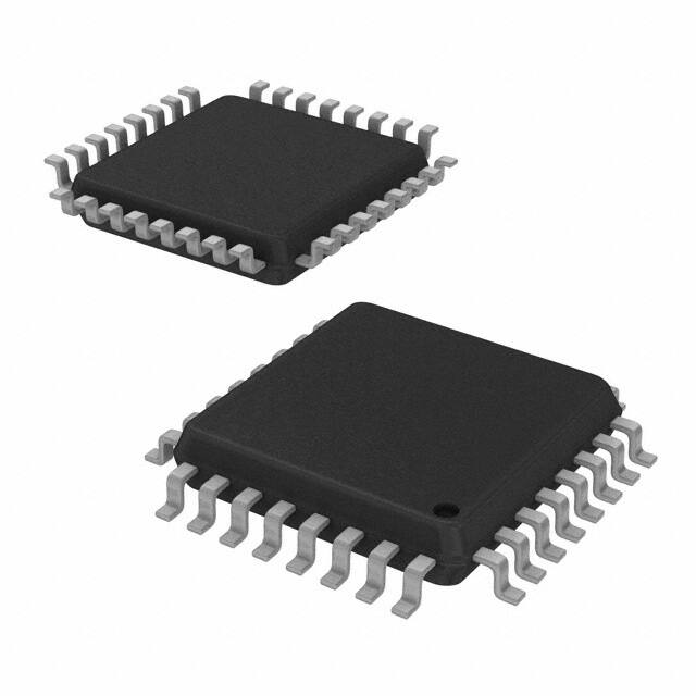
Intelligent Dynamic Clock Switch (IDCS)
PLL Clock Driver
MPC99J93
Product Discontinuance Notice – Last Time Buy Expires on (12/3/2013)
DATASHEET
The MPC99J93 is a PLL clock driver designed specifically for redundant clock
tree designs. The device receives two differential LVPECL clock signals from
which it generates five new differential LVPECL clock outputs. Two of the output
pairs regenerate the input signals frequency and phase while the other three
pairs generate 2x, phase aligned clock outputs.
MPC99J93
Features
•
•
•
•
•
•
Fully Integrated PLL
Intelligent Dynamic Clock Switch
LVPECL Clock Outputs
LVCMOS Control I/O
3.3-V Operation
32-Lead LQFP Packaging, Pb-Free
INTELLIGENT DYNAMIC
CLOCK SWITCH
PLL CLOCK DRIVER
Functional Description
The MPC99J93 Intelligent Dynamic Clock Switch (IDCS) circuit continuously
monitors both input CLK signals. Upon detection of a failure (CLK stuck HIGH or
LOW for at least 1 period), the INP_BAD for that CLK will be latched (H). If that
CLK is the primary clock, the IDCS will switch to the good secondary clock and
phase/frequency alignment will occur with minimal output phase disturbance.
The typical phase bump caused by a failed clock is eliminated. (See Applications
Information section).
AC SUFFIX
32-LEAD LQFP PACKAGE
Pb-FREE PACKAGE
CASE 873A-03
PLL_En
Clk_Selected
Inp1bad
DYNAMIC
SWITCH
LOGIC
Inp0bad
Man_Override
Alarm_Reset
Sel_Clk
Qb0
Qb0
OR
Qb1
Qb1
CLK0
CLK0
CLK1
CLK1
Ext_FB
Ext_FB
2
PLL
200 – 360 MHz
MR
4
Qb2
Qb2
Qa0
Qa0
Qa1
Qa1
Figure 1. Block Diagram
MPC99J93 REVISION 4 FEBRUARY 6, 2013
1
©2013 Integrated Device Technology, Inc.
�Qb0
Qb0
Qb1
Qb1
Qb2
Qb2
VCC
INTELLIGENT DYNAMIC CLOCK SWITCH (IDCS) PLL CLOCK DRIVER
VCC
MPC99J93 Data Sheet
24
23
22
21
20
19
18
17
Qa1
25
16
VCC
Qa1
26
15
Inp0bad
Qa0
27
14
Inp1bad
Qa0
28
13
Clk_Selected
VCC
29
12
GND
VCC_PLL
30
11
Ext_FB
Man_Override
31
10
Ext_FB
PLL_EN
32
MPC99J93
2
3
4
5
6
7
8
MR
Alarm_Reset
CLK0
CLK0
Sel_Clk
CLK1
CLK1
GND
9
1
GND
Figure 2. 32-Lead Pinout (Top View)
Table 1. Pin Descriptions
Pin Name
I/O
Pin Definition
CLK0, CLK0
CLK1, CLK1
LVPECL Input
LVPECL Input
Differential PLL clock reference (CLK0 pulldown, CLK0 pullup)
Differential PLL clock reference (CLK1 pulldown, CLK1 pullup)
Ext_FB, Ext_FB
LVPECL Input
Differential PLL feedback clock (Ext_FB pulldown, Ext_FB pullup)
Qa0:1, Qa0:1
LVPECL Output
Differential 1x output pairs. Connect one QAx pair to Ext_FB.
Qb0:2, Qb0:2
LVPECL Output
Differential 2x output pairs
Inp0bad
LVCMOS Output
Indicates detection of a bad input reference clock 0 with respect to the feedback signal. The output
is active HIGH and will remain HIGH until the alarm reset is asserted
Inp1bad
LVCMOS Output
Indicates detection of a bad input reference clock 1 with respect to the feedback signal. The output
is active HIGH and will remain HIGH until the alarm reset is asserted
Clk_Selected
LVCMOS Output
‘0' if clock 0 is selected, ‘1' if clock 1 is selected
Alarm_Reset
LVCMOS Input
‘0' will reset the input bad flags and align Clk_Selected with Sel_Clk. The input is “one-shotted”
(50k pullup)
Sel_Clk
LVCMOS Input
‘0' selects CLK0, ‘1' selects CLK1 (50k pulldown)
Manual_Override
LVCMOS Input
‘1' disables internal clock switch circuitry (50k pulldown)
PLL_En
LVCMOS Input
‘0' bypasses selected input reference around the phase-locked loop (50k pullup)
MR
LVCMOS Input
‘0' resets the internal dividers forcing Q outputs LOW. Asynchronous to the clock (50k pullup)
VCCA
Power Supply
PLL power supply
VCC
Power Supply
Digital power supply
GNDA
Power Supply
PLL ground
GND
Power Supply
Digital ground
MPC99J93 REVISION 4 FEBRUARY 6, 2013
2
©2013 Integrated Device Technology, Inc.
�MPC99J93 Data Sheet
INTELLIGENT DYNAMIC CLOCK SWITCH (IDCS) PLL CLOCK DRIVER
Table 2. Absolute Maximum Ratings(1)
Symbol
Characteristics
Min
Max
Unit
VCC
Supply Voltage
–0.3
3.9
V
VIN
DC Input Voltage
–0.3
VCC+0.3
V
DC Output Voltage
–0.3
VCC+0.3
V
DC Input Current
20
mA
DC Output Current
50
mA
125
C
VOUT
IIN
IOUT
TS
Storage Temperature
–65
1. Absolute maximum continuous ratings are those maximum values beyond which damage to the device may occur. Exposure to these
conditions or conditions beyond those indicated may adversely affect device reliability. Functional operation at absolute-maximum-rated
conditions is not implied.
Table 3. General Specifications
Symbol
Characteristics
Min
Typ
Max
VCC – 2
Unit
VTT
Output Termination Voltage
MM
ESD Protection (Machine model)
175
V
HBM
ESD Protection (Human body model)
1500
V
CDM
ESD Protection (Charged device model)
1000
V
LU
Latch-Up Immunity
100
mA
CIN
Input Capacitance
JA
Thermal Resistance Junction to Ambient
JESD 51-3, single layer test board
JC
Thermal Resistance Junction to Case
TJ
Operating Junction Temperature(1)
(continuous operation)
MTBF = 9.1 years
V
4.0
JESD 51-6, 2S2P multilayer test board
Condition
pF
Inputs
83.1
73.3
68.9
63.8
57.4
86.0
75.4
70.9
65.3
59.6
C/W
C/W
C/W
C/W
C/W
Natural convection
100 ft/min
200 ft/min
400 ft/min
800 ft/min
59.0
54.4
52.5
50.4
47.8
60.6
55.7
53.8
51.5
48.8
C/W
C/W
C/W
C/W
C/W
Natural convection
100 ft/min
200 ft/min
400 ft/min
800 ft/min
23.0
26.3
C/W
MIL-SPEC 883E
Method 1012.1
110
C
1. Operating junction temperature impacts device life time. Maximum continuous operating junction temperature should be selected according
to the application life time requirements (See application note AN1545 for more information). The device AC and DC parameters are
specified up to 110C junction temperature allowing the MPC99J93 to be used in applications requiring industrial temperature range. It is
recommended that users of the MPC99J93 employ thermal modeling analysis to assist in applying the junction temperature specifications
to their particular application.
MPC99J93 REVISION 4 FEBRUARY 6, 2013
3
©2013 Integrated Device Technology, Inc.
�MPC99J93 Data Sheet
INTELLIGENT DYNAMIC CLOCK SWITCH (IDCS) PLL CLOCK DRIVER
Table 4. DC Characteristics (VCC = 3.3 V ± 5%, TA = –40° to +85°C)
Symbol
Characteristics
Min
Typ
Max
Unit
Condition
VCC + 0.3
V
0.8
V
100
A
VIN = VCC or GND
V
IOH = -24 mA
0.55
V
IOL = 24 mA
0.1
1.3
V
Differential operation
VCC–1.8
VCC–0.3
V
Differential operation
100
A
VIN = VCC or GND
LVCMOS Control Inputs (MR, PLL_En, Sel_Clk, Man_Override, Alarm_Reset)
VIH
Input High Voltage
VIL
Input Low Voltage
IIN
Input Current(1)
2.0
LVCMOS Control Outputs (Clk_selected, Inp0bad, Inp1bad)
VOH
Output High Voltage
VOL
Output Low Voltage
2.0
LVPECL Clock Inputs (CLK0, CLK1, Ext_FB)(2)
VPP
VCMR
IIN
DC Differential Input Voltage(3)
Differential Cross Point
Input Current
Voltage(4)
(1)
LVPECL Clock Outputs (QA[1:0], QB[2:0])
VOH
Output High Voltage
VCC–1.20
VCC–0.95
VCC–0.70
V
Termination 50 to VTT
VOL
Output Low Voltage
VCC–1.90
VCC–1.75
VCC–1.45
V
Termination 50 to VTT
Maximum Power Supply Current
180
mA
GND pins
Maximum PLL Supply Current
15
mA
VCC_PLL pin
Supply Current
IGND
ICC_PLL
1.
2.
3.
4.
Inputs have internal pull-up/pull-down resistors affecting the input current.
Clock inputs driven by differential LVPECL compatible signals.
VPP is the minimum differential input voltage swing required to maintain AC characteristics.
VCMR (DC) is the crosspoint of the differential input signal. Functional operation is obtained when the crosspoint is within the VCMR (DC)
range and the input swing lies within the VPP (DC) specification.
MPC99J93 REVISION 4 FEBRUARY 6, 2013
4
©2013 Integrated Device Technology, Inc.
�MPC99J93 Data Sheet
INTELLIGENT DYNAMIC CLOCK SWITCH (IDCS) PLL CLOCK DRIVER
Table 5. AC Characteristics (VCC = 3.3 V 5%, TA = –40C to +85C)(1)
Symbol
fref
Characteristics
Input Reference Frequency
(2)
fVCO
VCO Frequency Range
fMAX
Output Frequency
frefDC
Reference Input Duty Cycle
t()
Propagation Delay
VPP
Differential Input Voltage(4)
Differential Input Crosspoint Voltage
tsk(O)
Output-to-Output Skew
DC
tJIT(CC)
tLOCK
tr, tf
Rate of Change of Period
Max
Unit
50
90
MHz
4 feedback
200
360
MHz
QA[1:0]
QB[2:0]
50
100
90
180
MHz
MHz
25
75
%
offset(3)
–0.15
0.9
+0.17
1.8
ns
ns
(peak-to-peak)
0.25
1.3
V
VCC–1.7
VCC–0.3
V
50
80
ps
ps
20
10
200
100
50
25
400
200
ps
ps
ps
ps
50
55
%
(5)
within QA[2:0] or QB[1:0]
within device
QA[1:0](6)
QB[2:0](6)
QA[1:0](7)
QB[2:0](7)
Output Duty Cycle
Cycle-to-Cycle Jitter
Typ
4 feedback
SPO, static phase
CLK0, CLK1 to any Q
VCMR
per/cycle
Min
45
RMS (1 )
25
Maximum PLL Lock Time
Output Rise/Fall Time
0.05
Condition
PLL locked
PLL locked
PLL_EN = 1
PLL_EN = 0
ps
10
ms
0.70
ns
20% to 80%
AC characteristics apply for parallel output termination of 50 to VCC – 2 V.
The input reference frequency must match the VCO lock range divided by the feedback divider ratio (FB): fref = fVCO FB.
CLK0, CLK1 to Ext_FB.
VPP is the minimum differential input voltage swing required to maintain AC characteristics including SPO and device-to-device skew.
Applicable to CLK0, CLK1 and Ext_FB.
5. VCMR (AC) is the crosspoint of the differential input signal. Normal AC operation is obtained when the crosspoint is within the VCMR (AC)
range and the input swing lies within the VPP (AC) specification. Violation of VCMR (AC) or VPP (AC) impacts the SPO, device and part-to-part
skew. Applicable to CLK0, CLK1 and Ext_FB.
6. Specification holds for a clock switch between two input signals (CLK0, CLK1) no greater than 400 ps out of phase. Delta period change per
cycle is averaged over the clock switch excursion.
7. Specification holds for a clock switch between two input signals (CLK0, CLK1) at any phase difference (180). Delta period change per
cycle is averaged over the clock switch excursion.
1.
2.
3.
4.
MPC99J93 REVISION 4 FEBRUARY 6, 2013
5
©2013 Integrated Device Technology, Inc.
�MPC99J93 Data Sheet
INTELLIGENT DYNAMIC CLOCK SWITCH (IDCS) PLL CLOCK DRIVER
APPLICATIONS INFORMATION
The MPC99J93 is a dual clock PLL with on-chip Intelligent
Dynamic Clock Switch (IDCS) circuitry.
both INP_BADs will be latched (H) after one Ext_FB period
and Clk_Selected will be latched (L) indicating CLK0 is the
PLL reference signal. While neither INP_BAD is latched (H),
the Clk_Selected can be freely changed with Sel_Clk.
Whenever a CLK switch occurs, (manually or by IDCS),
following the next negative edge of the newly selected PLL
reference signal, the next positive edge pair of Ext_FB and
the newly selected PLL reference signal will slew to
alignment.
To calculate the overall uncertainty between the input
CLKs and the outputs from multiple MPC99J93's, the
following procedure should be used. Assuming that the input
CLKs to all MPC9993's are exactly in phase, the total
uncertainty will be the sum of the static phase offset, max I/O
jitter, and output to output skew.
During a dynamic switch, the output phase between two
devices may be increased for a short period of time. If the two
input CLKs are 400ps out of phase, a dynamic switch of an
MPC99J93 will result in an instantaneous phase change of
400ps to the PLL reference signal without a corresponding
change in the output phase (due to the limited response of
the PLL). As a result, the I/O phase of a device, undergoing
this switch, will initially be 400ps and diminish as the PLL
slews to its new phase alignment. This transient timing issue
should be considered when analyzing the overall skew
budget of a system.
Definitions
primary clock: The input CLK selected by Sel_Clk.
secondary clock: The input CLK NOT selected by
Sel_Clk.
PLL reference signal: The CLK selected as the PLL
reference signal by Sel_Clk or IDCS. (IDCS can override
Sel_Clk).
Status Functions
Clk_Selected: Clk_Selected (L) indicates CLK0 is
selected as the PLL reference signal. Clk_Selected (H)
indicates CLK1 is selected as the PLL reference signal.
INP_BAD: Latched (H) when it's CLK is stuck (H) or (L) for
at least one Ext_FB period (Pos to Pos or Neg to Neg).
Cleared (L) on assertion of Alarm_Reset.
Control Functions
Sel_Clk: Sel_Clk (L) selects CLK0 as the primary clock.
Sel_Clk (H) selects CLK1 as the primary clock.
Alarm_Reset: Asserted by a negative edge. Generates a
one-shot reset pulse that clears INPUT_BAD latches and
Clk_Selected latch.
PLL_En: While (L), the PLL reference signal is substituted
for the VCO output.
MR: While (L), internal dividers are held in reset which
holds all Q outputs LOW.
Hot insertion and withdrawal
In PECL applications, a powered up driver will experience
a low impedance path through an MPC99J93 input to its
powered down VCC pins. In this case, a 100 ohm series
resistance should be used in front of the input pins to limit the
driver current. The resistor will have minimal impact on the
rise and fall times of the input signals.
Man Override (H)
(IDCS is disabled, PLL functions normally). PLL reference
signal (as indicated by Clk_Selected) will always be the CLK
selected by Sel_Clk. The status function INP_BAD is active
in Man Override (H) and (L).
Acquiring Frequency Lock
1. While the MPC99J93 is receiving a valid CLK signal,
assert Man_Override HIGH.
2. The PLL will phase and frequency lock within the
specified lock time.
3. Apply a HIGH to LOW transition to Alarm_Reset to reset
Input Bad flags.
4. De-assert Man_Override LOW to enable Intelligent
Dynamic Clock Switch mode.
Man Override (L)
(IDCS is enabled, PLL functions enhanced). The first CLK
to fail will latch it's INP_BAD (H) status flag and select the
other input as the Clk_Selected for the PLL reference clock.
Once latched, the Clk_Selected and INP_BAD remain
latched until assertion of Alarm_Reset which clears all
latches (INP_BADs are cleared and Clk_Selected = Sel_Clk).
NOTE: If both CLKs are bad when Alarm_Reset is asserted,
MPC99J93 REVISION 4 FEBRUARY 6, 2013
6
©2013 Integrated Device Technology, Inc.
�MPC99J93 Data Sheet
INTELLIGENT DYNAMIC CLOCK SWITCH (IDCS) PLL CLOCK DRIVER
PACKAGE DIMENSIONS
4X
0.20 H
6
A-B D
D1
PIN 1 INDEX
3
e/2
D1/2
32
A, B, D
25
1
E1/2 A
F
B
6 E1
E
4
F
DETAIL G
8
17
9
7
D/2
NOTES:
1. DIMENSIONS ARE IN MILLIMETERS.
2. INTERPRET DIMENSIONS AND TOLERANCES PER
ASME Y14.5M, 1994.
3. DATUMS A, B, AND D TO BE DETERMINED AT
DATUM PLANE H.
4. DIMENSIONS D AND E TO BE DETERMINED AT
SEATING PLANE C.
5. DIMENSION b DOES NOT INCLUDE DAMBAR
PROTRUSION. ALLOWABLE DAMBAR PROTRUSION
SHALL NOT CAUSE THE LEAD WIDTH TO EXCEED
THE MAXIMUM b DIMENSION BY MORE THAN
0.08-mm. DAMBAR CANNOT BE LOCATED ON THE
LOWER RADIUS OR THE FOOT. MINIMUM SPACE
BETWEEN PROTRUSION AND ADJACENT LEAD OR
PROTRUSION: 0.07-mm.
6. DIMENSIONS D1 AND E1 DO NOT INCLUDE MOLD
PROTRUSION. ALLOWABLE PROTRUSION IS
0.25-mm PER SIDE. D1 AND E1 ARE MAXIMUM
PLASTIC BODY SIZE DIMENSIONS INCLUDING
MOLD MISMATCH.
7. EXACT SHAPE OF EACH CORNER IS OPTIONAL.
8. THESE DIMENSIONS APPLY TO THE FLAT
SECTION OF THE LEAD BETWEEN 0.1-mm AND
0.25-mm FROM THE LEAD TIP.
4
D
A-B D
H
SEATING
PLANE
DETAIL G
D
4X
0.20 C
E/2
28X
e
32X
C
0.1 C
DETAIL AD
PLATING
BASE
METAL
b1
c
c1
b
8X
(θ1˚)
0.20
R R2
A2
5
8
C A-B D
SECTION F-F
R R1
A
M
0.25
GAUGE PLANE
A1
(S)
L
(L1)
θ˚
DETAIL AD
DIM
A
A1
A2
b
b1
c
c1
D
D1
e
E
E1
L
L1
q
q1
R1
R2
S
MILLIMETERS
MIN
MAX
1.40
1.60
0.05
0.15
1.35
1.45
0.30
0.45
0.30
0.40
0.09
0.20
0.09
0.16
9.00 BSC
7.00 BSC
0.80 BSC
9.00 BSC
7.00 BSC
0.50
0.70
1.00 REF
0˚
7˚
12 REF
0.08
0.20
0.08
--0.20 REF
CASE 873A-03
ISSUE B
32-LEAD LQFP PACKAGE
MPC99J93 REVISION 4 FEBRUARY 6, 2013
7
©2013 Integrated Device Technology, Inc.
�MPC99J93 Data Sheet
INTELLIGENT DYNAMIC CLOCK SWITCH (IDCS) PLL CLOCK DRIVER
Revision History Sheet
Rev
4
Table
Page
1
Description of Change
Date
Product Discontinuance Notice – Last Time Buy Expires on (12/3/2013)
MPC99J93 REVISION 4 FEBRUARY 6, 2013
8
2/6/2013
©2013 Integrated Device Technology, Inc.
�MPC99J93 Data Sheet
INTELLIGENT DYNAMIC CLOCK SWITCH (IDCS) PLL CLOCK DRIVER
We’ve Got Your Timing Solution
6024 Silver Creek Valley Road
San Jose, California 95138
Sales
800-345-7015 (inside USA)
+408-284-8200 (outside USA)
Fax: 408-284-2775
www.IDT.com/go/contactIDT
Technical Support
netcom@idt.com
+480-763-2056
DISCLAIMER Integrated Device Technology, Inc. (IDT) and its subsidiaries reserve the right to modify the products and/or specifications described herein at any time and at IDT’s sole discretion. All information in this document,
including descriptions of product features and performance, is subject to change without notice. Performance specifications and the operating parameters of the described products are determined in the independent state and are not
guaranteed to perform the same way when installed in customer products. The information contained herein is provided without representation or warranty of any kind, whether express or implied, including, but not limited to, the
suitability of IDT’s products for any particular purpose, an implied warranty of merchantability, or non-infringement of the intellectual property rights of others. This document is presented only as a guide and does not convey any
license under intellectual property rights of IDT or any third parties.
IDT’s products are not intended for use in applications involving extreme environmental conditions or in life support systems or similar devices where the failure or malfunction of an IDT product can be reasonably expected to significantly affect the health or safety of users. Anyone using an IDT product in such a manner does so at their own risk, absent an express, written agreement by IDT.
Integrated Device Technology, IDT and the IDT logo are registered trademarks of IDT. Other trademarks and service marks used herein, including protected names, logos and designs, are the property of IDT or their respective third
party owners.
Copyright 2013. All rights reserved.
�IMPORTANT NOTICE AND DISCLAIMER
RENESAS ELECTRONICS CORPORATION AND ITS SUBSIDIARIES (“RENESAS”) PROVIDES TECHNICAL
SPECIFICATIONS AND RELIABILITY DATA (INCLUDING DATASHEETS), DESIGN RESOURCES (INCLUDING
REFERENCE DESIGNS), APPLICATION OR OTHER DESIGN ADVICE, WEB TOOLS, SAFETY INFORMATION, AND
OTHER RESOURCES “AS IS” AND WITH ALL FAULTS, AND DISCLAIMS ALL WARRANTIES, EXPRESS OR IMPLIED,
INCLUDING, WITHOUT LIMITATION, ANY IMPLIED WARRANTIES OF MERCHANTABILITY, FITNESS FOR A
PARTICULAR PURPOSE, OR NON-INFRINGEMENT OF THIRD PARTY INTELLECTUAL PROPERTY RIGHTS.
These resources are intended for developers skilled in the art designing with Renesas products. You are solely responsible
for (1) selecting the appropriate products for your application, (2) designing, validating, and testing your application, and (3)
ensuring your application meets applicable standards, and any other safety, security, or other requirements. These
resources are subject to change without notice. Renesas grants you permission to use these resources only for
development of an application that uses Renesas products. Other reproduction or use of these resources is strictly
prohibited. No license is granted to any other Renesas intellectual property or to any third party intellectual property.
Renesas disclaims responsibility for, and you will fully indemnify Renesas and its representatives against, any claims,
damages, costs, losses, or liabilities arising out of your use of these resources. Renesas' products are provided only subject
to Renesas' Terms and Conditions of Sale or other applicable terms agreed to in writing. No use of any Renesas resources
expands or otherwise alters any applicable warranties or warranty disclaimers for these products.
(Rev.1.0 Mar 2020)
Corporate Headquarters
Contact Information
TOYOSU FORESIA, 3-2-24 Toyosu,
Koto-ku, Tokyo 135-0061, Japan
www.renesas.com
For further information on a product, technology, the most
up-to-date version of a document, or your nearest sales
office, please visit:
www.renesas.com/contact/
Trademarks
Renesas and the Renesas logo are trademarks of Renesas
Electronics Corporation. All trademarks and registered
trademarks are the property of their respective owners.
© 2020 Renesas Electronics Corporation. All rights reserved.
�