Data Sheet
NE3521M04
N-Channel GaAs HJ-FET, K Band Low Noise and High-Gain
R09DS0058EJ0100
Rev.1.00
Mar 19, 2013
FEATURES
• Low noise figure and high associated gain:
NF = 0.85 dB TYP., Ga = 11 dB TYP. @ VDS = 2 V, ID = 10 mA, f = 20 GHz
NF = 0.9 dB TYP., Ga = 10.5 dB TYP. @VDS = 2 V, ID = 6mA, f = 20 GHz (Reference Value)
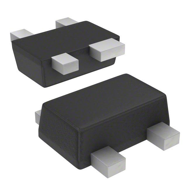
• Flat-lead 4-pin thin-type super minimold (M04) package
APPLICATIONS
• DBS LNB gain-stage, Mix-stage
• Low noise amplifier for microwave communication system
ORDERING INFORMATION
Part Number
NE3521M04-T2
Order Number
NE3521M04-T2-A
NE3521M04-T2B
NE3521M04-T2B-A
Package
Quantity
Flat-lead 4-pin 3 kpcs/reel
thin-type super
minimold (M04)
15 kpcs/reel
(Pb-Free)
Marking
V86
Supplying Form
• Embossed tape 8 mm wide
• Pin 1 (Source), Pin 2 (Drain)
face the perforation side of the
tape
Remark To order evaluation samples, contact your nearby sales office.
Part number for sample order: NE3521M04
ABSOLUTE MAXIMUM RATINGS (TA = +25°C, unless otherwise specified)
Symbol
Ratings
Unit
Drain to Source Voltage
Parameter
VDS
4.0
V
Gate to Source Voltage
VGS
–3.0
V
Drain Current
ID
IDSS
mA
Gate Current
IG
80
μA
Ptot
125
mW
Tch
+125
°C
Total Power Dissipation
Note
Channel Temperature
Storage Temperature
Tstg
–65 to +125
2
Note: Mounted on 1.08 cm × 1.0 mm (t) glass epoxy PWB
°C
CAUTION
Observe precautions when handling because these devices are sensitive to electrostatic discharge.
R09DS0058EJ0100 Rev.1.00
Mar 19, 2013
Page 1 of 8
�NE3521M04
RECOMMENDED OPERATING RANGE (TA = +25°C, unless otherwise specified)
Parameter
Symbol
MIN.
TYP.
MAX.
Unit
VDS
1
2
3
V
Drain Current
ID
3
10
15
mA
Input Power
Pin
–
–
0
dBm
Drain to Source Voltage
ELECTRICAL CHARACTERISTICS (TA = +25°C, unless otherwise specified)
MIN.
TYP.
MAX.
Unit
Gate to Source Leak Current
Parameter
IGSO
VGS = –3.0 V
–
0.5
10
μA
Saturated Drain Current
IDSS
VDS = 2 V, VGS = 0 V
25
45
70
mA
Gate to Source Cut-off Voltage
Symbol
Test Conditions
VGS (off)
VDS = 2 V, ID = 100 μA
–0.2
–0.7
–1.3
V
Transconductance
gm
VDS = 2 V, ID = 10 mA
50
–
–
mS
Noise Figure
NF
VDS = 2 V, ID = 10 mA, f = 20 GHz
–
0.85
1.2
dB
Associated Gain
Ga
9
11
–
dB
STANDARD CHARACTERISTICS FOR REFERENCE
(TA = +25°C, unless otherwise specified)
Parameter
Symbol
Noise Figure
NF
Associated Gain
Ga
R09DS0058EJ0100 Rev.1.00
Mar 19, 2013
Test Conditions
VDS = 2 V, ID = 6 mA, f = 20 GHz
Reference Value
0.9
Unit
dB
10.5
dB
Page 2 of 8
�NE3521M04
TYPICAL CHARACTERISTICS (TA = +25°C, unless otherwise specified)
TOTAL POWER DISSIPATION
vs. AMBIENT TEMPERATURE
DRAIN CURRENT vs.
GATE TO SOURCE VOLTAGE
80
VDS = 2 V
DRAIN CURRENT ID (mA)
70
200
150
125
100
50
0
200
100 125 150
50
50
40
30
20
0
-0.80
250
-0.60
-0.40
-0.20
0.00
Ambient Temperature TA (°C)
GATE TO SOURCE VOLTAGE VGS (V)
MINIMUM NOISE FIGURE,
ASSOCIATED GAIN vs.DRAIN CURRENT
DRAIN CURRENT
vs. DRAIN TO SOURCE VOLTAGE
2.5
f = 20 GHz
VDS = 2 V
Ga
2.0
14
80
13
70
12
11
1.5
10
9
1.0
8
7
NFmin
0.5
6
5
0.0
0
4
5
10
15
20
25
DRAIN CURRENT ID (mA)
MINIMUM NOISE FIGURE NFmin (dB)
60
10
ASSOCIATED GAIN Ga (dB)
Total Power Dissipation Ptot (mW)
250
60
50
-0.1 V
30
-0.2 V
20
-0.3 V
10
0
30
VGS = 0 V
40
-0.4 V
-0.5 V
0.0
1.0
2.0
3.0
4.0
DRAIN TO SOURCE VOLTAGE VDS (V)
DRAIN CURRENT ID (mA)
2.0
20
VDS = 2 V
ID = 10 mA
1.8
18
1.6
16
1.4
14
Ga
1.2
12
1.0
10
0.8
8
0.6
6
NFmin
0.4
4
0.2
0.0
2
5
10
15
20
25
30
ASSOCIATED GAIN Ga (dB)
MINIMUM NOISE FIGURE NFmin (dB)
MINIMUM NOISE FIGURE,
ASSOCIATED GAIN vs.FREQUENCY
0
FREQUENCY f (GHz)
Remark The graphs indicate nominal characteristics.
R09DS0058EJ0100 Rev.1.00
Mar 19, 2013
Page 3 of 8
�NE3521M04
S-PARAMETERS
S-parameters and noise parameters are provided on our web site in a form (S2P) that enables direct import of the
parameters to microwave circuit simulators without the need for keyboard inputs.
Click here to download S-parameters.
[Products] → [RF Devices] → [Device Parameters]
URL http://www.renesas.com/products/microwave/
R09DS0058EJ0100 Rev.1.00
Mar 19, 2013
Page 4 of 8
�NE3521M04
PACKAGE DIMENSIONS
FLAT-LEAD 4-PIN THIN-TYPE SUPER MINIMOLD (M04) (UNIT: mm)
2.0±0.1
2
1
1.25
3
4
1.30
0.65
1.30
3
4
0.30+0.1
–0.05
0.11+0.1
–0.05
1
0.30+0.1
–0.05
0.59±0.05
(1.05)
0.65
0.60
0.65
1.25
2
1.25±0.1
V86
2.0±0.1
(Bottom View)
0.30+0.1
–0.05
0.40+0.1
–0.05
2.05±0.1
PIN CONNECTIONS
1.
2.
3.
4.
R09DS0058EJ0100 Rev.1.00
Mar 19, 2013
Source
Drain
Source
Gate
Page 5 of 8
�NE3521M04
MOUNTING PAD DIMENSIONS
FLAT-LEAD 4-PIN THIN-TYPE SUPER MINIMOLD (M04) (UNIT: mm)
-Reference 1-
1.35
0.60
0.75
1
4
0.
2
4 - φ0.50
0.
0.58
Device Direction
28
1
1.20
1.42
0.56
4
1.26
1.20
4
2
2
38
0.
42
3
0.
0.80
3
0.75
0.60
1.35
-Reference 2Device Direction
3
2
3
4
1
4
0.5
1
1.3
1.25
0.6
2
1.6
0.6
Remark The mounting pad layout in this document is for reference only.
R09DS0058EJ0100 Rev.1.00
Mar 19, 2013
Page 6 of 8
�NE3521M04
RECOMMENDED SOLDERING CONDITIONS
This product should be soldered and mounted under the following recommended conditions. For soldering methods and
conditions other than those recommended below, contact your nearby sales office.
Soldering Method
Infrared Reflow
Partial Heating
Soldering Conditions
Peak temperature (package surface temperature)
Time at peak temperature
Time at temperature of 220°C or higher
Preheating time at 120 to 180°C
Maximum number of reflow processes
Maximum chlorine content of rosin flux (% mass)
: 260°C or below
: 10 seconds or less
: 60 seconds or less
: 120±30 seconds
: 3 times
: 0.2% (Wt.) or below
Peak temperature (package surface temperature) : 350°C or below
Soldering time (per side of device)
: 3 seconds or less
Maximum chlorine content of rosin flux (% mass) : 0.2% (Wt.) or below
Condition Symbol
IR260
HS350
CAUTION
Do not use different soldering methods together (except for partial heating).
R09DS0058EJ0100 Rev.1.00
Mar 19, 2013
Page 7 of 8
�NE3521M04
Caution
GaAs Products
This product uses gallium arsenide (GaAs).
GaAs vapor and powder are hazardous to human health if inhaled or ingested, so please observe
the following points.
• Follow related laws and ordinances when disposing of the product. If there are no applicable laws
and/or ordinances, dispose of the product as recommended below.
1. Commission a disposal company able to (with a license to) collect, transport and dispose of
materials that contain arsenic and other such industrial waste materials.
2. Exclude the product from general industrial waste and household garbage, and ensure that the
product is controlled (as industrial waste subject to special control) up until final disposal.
• Do not burn, destroy, cut, crush, or chemically dissolve the product.
• Do not lick the product or in any way allow it to enter the mouth.
R09DS0058EJ0100 Rev.1.00
Mar 19, 2013
Page 8 of 8
�Revision History
Rev.
1.00
Date
Mar 19, 2013
NE3521M04 Data Sheet
Description
Summary
Page
-
First edition issued
All trademarks and registered trademarks are the property of their respective owners.
C-1
�Notice
1.
Descriptions of circuits, software and other related information in this document are provided only to illustrate the operation of semiconductor products and application examples. You are fully responsible for
the incorporation of these circuits, software, and information in the design of your equipment. Renesas Electronics assumes no responsibility for any losses incurred by you or third parties arising from the
use of these circuits, software, or information.
2.
Renesas Electronics has used reasonable care in preparing the information included in this document, but Renesas Electronics does not warrant that such information is error free. Renesas Electronics
3.
Renesas Electronics does not assume any liability for infringement of patents, copyrights, or other intellectual property rights of third parties by or arising from the use of Renesas Electronics products or
assumes no liability whatsoever for any damages incurred by you resulting from errors in or omissions from the information included herein.
technical information described in this document. No license, express, implied or otherwise, is granted hereby under any patents, copyrights or other intellectual property rights of Renesas Electronics or
others.
4.
You should not alter, modify, copy, or otherwise misappropriate any Renesas Electronics product, whether in whole or in part. Renesas Electronics assumes no responsibility for any losses incurred by you or
5.
Renesas Electronics products are classified according to the following two quality grades: "Standard" and "High Quality". The recommended applications for each Renesas Electronics product depends on
third parties arising from such alteration, modification, copy or otherwise misappropriation of Renesas Electronics product.
the product's quality grade, as indicated below.
"Standard": Computers; office equipment; communications equipment; test and measurement equipment; audio and visual equipment; home electronic appliances; machine tools; personal electronic
equipment; and industrial robots etc.
"High Quality": Transportation equipment (automobiles, trains, ships, etc.); traffic control systems; anti-disaster systems; anti-crime systems; and safety equipment etc.
Renesas Electronics products are neither intended nor authorized for use in products or systems that may pose a direct threat to human life or bodily injury (artificial life support devices or systems, surgical
implantations etc.), or may cause serious property damages (nuclear reactor control systems, military equipment etc.). You must check the quality grade of each Renesas Electronics product before using it
in a particular application. You may not use any Renesas Electronics product for any application for which it is not intended. Renesas Electronics shall not be in any way liable for any damages or losses
incurred by you or third parties arising from the use of any Renesas Electronics product for which the product is not intended by Renesas Electronics.
6.
You should use the Renesas Electronics products described in this document within the range specified by Renesas Electronics, especially with respect to the maximum rating, operating supply voltage
range, movement power voltage range, heat radiation characteristics, installation and other product characteristics. Renesas Electronics shall have no liability for malfunctions or damages arising out of the
use of Renesas Electronics products beyond such specified ranges.
7.
Although Renesas Electronics endeavors to improve the quality and reliability of its products, semiconductor products have specific characteristics such as the occurrence of failure at a certain rate and
malfunctions under certain use conditions. Further, Renesas Electronics products are not subject to radiation resistance design. Please be sure to implement safety measures to guard them against the
possibility of physical injury, and injury or damage caused by fire in the event of the failure of a Renesas Electronics product, such as safety design for hardware and software including but not limited to
redundancy, fire control and malfunction prevention, appropriate treatment for aging degradation or any other appropriate measures. Because the evaluation of microcomputer software alone is very difficult,
please evaluate the safety of the final products or systems manufactured by you.
8.
Please contact a Renesas Electronics sales office for details as to environmental matters such as the environmental compatibility of each Renesas Electronics product. Please use Renesas Electronics
products in compliance with all applicable laws and regulations that regulate the inclusion or use of controlled substances, including without limitation, the EU RoHS Directive. Renesas Electronics assumes
no liability for damages or losses occurring as a result of your noncompliance with applicable laws and regulations.
9.
Renesas Electronics products and technology may not be used for or incorporated into any products or systems whose manufacture, use, or sale is prohibited under any applicable domestic or foreign laws or
regulations. You should not use Renesas Electronics products or technology described in this document for any purpose relating to military applications or use by the military, including but not limited to the
development of weapons of mass destruction. When exporting the Renesas Electronics products or technology described in this document, you should comply with the applicable export control laws and
regulations and follow the procedures required by such laws and regulations.
10. It is the responsibility of the buyer or distributor of Renesas Electronics products, who distributes, disposes of, or otherwise places the product with a third party, to notify such third party in advance of the
contents and conditions set forth in this document, Renesas Electronics assumes no responsibility for any losses incurred by you or third parties as a result of unauthorized use of Renesas Electronics
products.
11. This document may not be reproduced or duplicated in any form, in whole or in part, without prior written consent of Renesas Electronics.
12. Please contact a Renesas Electronics sales office if you have any questions regarding the information contained in this document or Renesas Electronics products, or if you have any other inquiries.
(Note 1)
"Renesas Electronics" as used in this document means Renesas Electronics Corporation and also includes its majority-owned subsidiaries.
(Note 2)
"Renesas Electronics product(s)" means any product developed or manufactured by or for Renesas Electronics.
http://www.renesas.com
SALES OFFICES
Refer to "http://www.renesas.com/" for the latest and detailed information.
California Eastern Laboratories, Inc.
4590 Patrick Henry Drive, Santa Clara, California 95054, U.S.A.
Tel: +1-408-919-2500, Fax: +1-408-988-0279
Renesas Electronics Europe Limited
Dukes Meadow, Millboard Road, Bourne End, Buckinghamshire, SL8 5FH, U.K
Tel: +44-1628-651-700, Fax: +44-1628-651-804
Renesas Electronics Europe GmbH
Arcadiastrasse 10, 40472 Düsseldorf, Germany
Tel: +49-211-65030, Fax: +49-211-6503-1327
Renesas Electronics (China) Co., Ltd.
7th Floor, Quantum Plaza, No.27 ZhiChunLu Haidian District, Beijing 100083, P.R.China
Tel: +86-10-8235-1155, Fax: +86-10-8235-7679
Renesas Electronics (Shanghai) Co., Ltd.
Unit 204, 205, AZIA Center, No.1233 Lujiazui Ring Rd., Pudong District, Shanghai 200120, China
Tel: +86-21-5877-1818, Fax: +86-21-6887-7858 / -7898
Renesas Electronics Hong Kong Limited
Unit 1601-1613, 16/F., Tower 2, Grand Century Place, 193 Prince Edward Road West, Mongkok, Kowloon, Hong Kong
Tel: +852-2886-9318, Fax: +852 2886-9022/9044
Renesas Electronics Taiwan Co., Ltd.
13F, No. 363, Fu Shing North Road, Taipei, Taiwan
Tel: +886-2-8175-9600, Fax: +886 2-8175-9670
Renesas Electronics Singapore Pte. Ltd.
80 Bendemeer Road, Unit #06-02 Hyflux Innovation Centre Singapore 339949
Tel: +65-6213-0200, Fax: +65-6213-0300
Renesas Electronics Malaysia Sdn.Bhd.
Unit 906, Block B, Menara Amcorp, Amcorp Trade Centre, No. 18, Jln Persiaran Barat, 46050 Petaling Jaya, Selangor Darul Ehsan, Malaysia
Tel: +60-3-7955-9390, Fax: +60-3-7955-9510
Renesas Electronics Korea Co., Ltd.
11F., Samik Lavied' or Bldg., 720-2 Yeoksam-Dong, Kangnam-Ku, Seoul 135-080, Korea
Tel: +82-2-558-3737, Fax: +82-2-558-5141
© 2013 Renesas Electronics Corporation. All rights reserved.
[Colophon 2.2]
�