To our customers,
Old Company Name in Catalogs and Other Documents
On April 1st, 2010, NEC Electronics Corporation merged with Renesas Technology
Corporation, and Renesas Electronics Corporation took over all the business of both
companies. Therefore, although the old company name remains in this document, it is a valid
Renesas Electronics document. We appreciate your understanding.
Renesas Electronics website: http://www.renesas.com
April 1st, 2010
Renesas Electronics Corporation
Issued by: Renesas Electronics Corporation (http://www.renesas.com)
Send any inquiries to http://www.renesas.com/inquiry.
�Notice
1.
2.
3.
4.
5.
6.
7.
All information included in this document is current as of the date this document is issued. Such information, however, is
subject to change without any prior notice. Before purchasing or using any Renesas Electronics products listed herein, please
confirm the latest product information with a Renesas Electronics sales office. Also, please pay regular and careful attention to
additional and different information to be disclosed by Renesas Electronics such as that disclosed through our website.
Renesas Electronics does not assume any liability for infringement of patents, copyrights, or other intellectual property rights
of third parties by or arising from the use of Renesas Electronics products or technical information described in this document.
No license, express, implied or otherwise, is granted hereby under any patents, copyrights or other intellectual property rights
of Renesas Electronics or others.
You should not alter, modify, copy, or otherwise misappropriate any Renesas Electronics product, whether in whole or in part.
Descriptions of circuits, software and other related information in this document are provided only to illustrate the operation of
semiconductor products and application examples. You are fully responsible for the incorporation of these circuits, software,
and information in the design of your equipment. Renesas Electronics assumes no responsibility for any losses incurred by
you or third parties arising from the use of these circuits, software, or information.
When exporting the products or technology described in this document, you should comply with the applicable export control
laws and regulations and follow the procedures required by such laws and regulations. You should not use Renesas
Electronics products or the technology described in this document for any purpose relating to military applications or use by
the military, including but not limited to the development of weapons of mass destruction. Renesas Electronics products and
technology may not be used for or incorporated into any products or systems whose manufacture, use, or sale is prohibited
under any applicable domestic or foreign laws or regulations.
Renesas Electronics has used reasonable care in preparing the information included in this document, but Renesas Electronics
does not warrant that such information is error free. Renesas Electronics assumes no liability whatsoever for any damages
incurred by you resulting from errors in or omissions from the information included herein.
Renesas Electronics products are classified according to the following three quality grades: “Standard”, “High Quality”, and
“Specific”. The recommended applications for each Renesas Electronics product depends on the product’s quality grade, as
indicated below. You must check the quality grade of each Renesas Electronics product before using it in a particular
application. You may not use any Renesas Electronics product for any application categorized as “Specific” without the prior
written consent of Renesas Electronics. Further, you may not use any Renesas Electronics product for any application for
which it is not intended without the prior written consent of Renesas Electronics. Renesas Electronics shall not be in any way
liable for any damages or losses incurred by you or third parties arising from the use of any Renesas Electronics product for an
application categorized as “Specific” or for which the product is not intended where you have failed to obtain the prior written
consent of Renesas Electronics. The quality grade of each Renesas Electronics product is “Standard” unless otherwise
expressly specified in a Renesas Electronics data sheets or data books, etc.
Computers; office equipment; communications equipment; test and measurement equipment; audio and visual
equipment; home electronic appliances; machine tools; personal electronic equipment; and industrial robots.
“High Quality”: Transportation equipment (automobiles, trains, ships, etc.); traffic control systems; anti-disaster systems; anticrime systems; safety equipment; and medical equipment not specifically designed for life support.
“Specific”:
Aircraft; aerospace equipment; submersible repeaters; nuclear reactor control systems; medical equipment or
systems for life support (e.g. artificial life support devices or systems), surgical implantations, or healthcare
intervention (e.g. excision, etc.), and any other applications or purposes that pose a direct threat to human life.
You should use the Renesas Electronics products described in this document within the range specified by Renesas Electronics,
especially with respect to the maximum rating, operating supply voltage range, movement power voltage range, heat radiation
characteristics, installation and other product characteristics. Renesas Electronics shall have no liability for malfunctions or
damages arising out of the use of Renesas Electronics products beyond such specified ranges.
Although Renesas Electronics endeavors to improve the quality and reliability of its products, semiconductor products have
specific characteristics such as the occurrence of failure at a certain rate and malfunctions under certain use conditions. Further,
Renesas Electronics products are not subject to radiation resistance design. Please be sure to implement safety measures to
guard them against the possibility of physical injury, and injury or damage caused by fire in the event of the failure of a
Renesas Electronics product, such as safety design for hardware and software including but not limited to redundancy, fire
control and malfunction prevention, appropriate treatment for aging degradation or any other appropriate measures. Because
the evaluation of microcomputer software alone is very difficult, please evaluate the safety of the final products or system
manufactured by you.
Please contact a Renesas Electronics sales office for details as to environmental matters such as the environmental
compatibility of each Renesas Electronics product. Please use Renesas Electronics products in compliance with all applicable
laws and regulations that regulate the inclusion or use of controlled substances, including without limitation, the EU RoHS
Directive. Renesas Electronics assumes no liability for damages or losses occurring as a result of your noncompliance with
applicable laws and regulations.
This document may not be reproduced or duplicated, in any form, in whole or in part, without prior written consent of Renesas
Electronics.
Please contact a Renesas Electronics sales office if you have any questions regarding the information contained in this
document or Renesas Electronics products, or if you have any other inquiries.
“Standard”:
8.
9.
10.
11.
12.
(Note 1) “Renesas Electronics” as used in this document means Renesas Electronics Corporation and also includes its majorityowned subsidiaries.
(Note 2) “Renesas Electronics product(s)” means any product developed or manufactured by or for Renesas Electronics.
�DATA SHEET
SILICON POWER MOS FET
NE5500234
N-CHANNEL SILICON POWER MOS FET
POWER AMPLIFIER FOR DCS1800/PCS1900 HANDSETS
DESCRIPTION
The NE5500234 is an N-channel silicon power MOS FET specially designed as the transmission power amplifier
for DCS1800 and PCS1900 handsets. Dies are manufactured using our NEWMOS technology (our 0.6 μm WSi gate
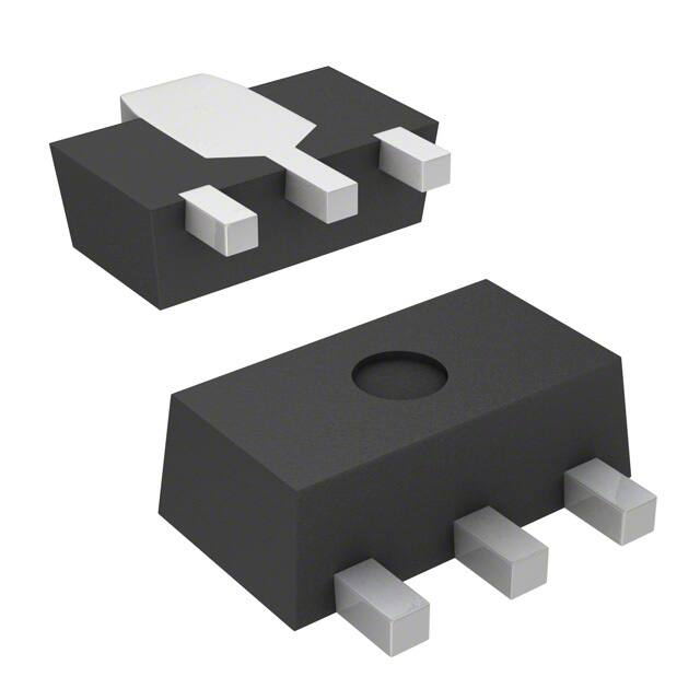
lateral MOS FET), housed in a surface mount 3-pin power Minimold (34 PKG) (SOT-89 type) package. The device
can deliver 32.5 dBm output power with 50% power added efficiency at 1.9 GHz under the 4.8 V supply voltage.
FEATURES
• High output power
: Pout = 32.5 dBm TYP. (VDS = 4.8 V, IDset = 400 mA, f = 1.9 GHz, Pin = 25 dBm)
• High power added efficiency : ηadd = 50% TYP. (VDS = 4.8 V, IDset = 400 mA, f = 1.9 GHz, Pin = 25 dBm)
• High linear gain
: GL = 11 dB TYP. (VDS = 4.8 V, IDset = 400 mA, f = 1.9 GHz)
• Surface mount package
: 3-pin power Minimold (34 PKG) (SOT-89 type)
• Single supply
: VDS = 3.0 to 6.0 V
APPLICATIONS
• Digital cellular phones
: DCS1800/PCS1900 handsets
• Handheld transceiver
: FRS (Family Radio Service), GMRS (General Mobile Radio Service)
• Others
: General purpose amplifiers for various applications
ORDERING INFORMATION
Part Number
NE5500234
Order Number
NE5500234-AZ
Package
Marking
3-pin power minimold
V2
(SOT-89, Our code: 34)
Supplying Form
• Magazine case
• Qty 25 pcs/case
(Pb-Free : External
solder plating)
NE5500234-T1
NE5500234-T1-AZ
3-pin power minimold
(SOT-89, Our code: 34)
(Pb-Free : External
• 12 mm wide embossed taping
• Source pin face the perforation side of the tape
• Qty 1 kpcs/reel
solder plating)
Remarks 1. To order evaluation samples, contact your nearby sales office.
Part number for sample order: NE5500234
2. This product is containing Pb-material inside.
Caution Observe precautions when handling because these devices are sensitive to electrostatic discharge.
The information in this document is subject to change without notice. Before using this document, please
confirm that this is the latest version.
Not all products and/or types are available in every country. Please check with an NEC Electronics
sales representative for availability and additional information.
Document No. PU10405EJ02V0DS (2nd edition)
Date Published August 2007 NS
Printed in Japan
The mark shows major revised points.
The revised points can be easily searched by copying an "" in the PDF file and specifying it in the "Find what:" field.
2004, 2007
�NE5500234
ABSOLUTE MAXIMUM RATINGS (TA = +25°C)
Operation in excess of any one of these parameters may result in permanent damage.
Parameter
Symbol
Ratings
Unit
Drain to Source Voltage
VDS
20
V
Gate to Source Voltage
VGS
6.0
V
ID
1.0
A
Total Power Dissipation
Ptot
10
W
Channel Temperature
Tch
125
°C
Storage Temperature
Tstg
−65 to +125
°C
Test Conditions
MIN.
TYP.
MAX.
Unit
Drain Current
RECOMMENDED OPERATING CONDITIONS
Parameter
Symbol
Drain to Source Voltage
VDS
3.0
4.8
6.0
V
Gate to Source Voltage
VGS
0
2.0
3.5
V
Drain Current
ID
Duty Cycle ≤ 50%, Ton ≤ 1 s
−
0.75
1.0
A
Input Power
Pin
f = 1.9 GHz, VDS = 4.8 V
−
−
27
dBm
MIN.
TYP.
MAX.
Unit
ELECTRICAL CHARACTERISTICS
(TA = +25°C, unless otherwise specified, using our standard test fixture.)
Parameter
Symbol
Test Conditions
Gate to Source Leakage Current
IGSO
VGS = 6.0 V
−
−
100
nA
Drain to Source Leakage Current
(Zero Gate Voltage Drain Current)
IDSS
VDS = 8.5 V
−
−
100
nA
Gate Threshold Voltage
Vth
VDS = 4.8 V, IDS = 1 mA
1.0
1.4
2.0
V
Thermal Resistance
Rth
Channel to Case
−
10
−
°C/W
Transconductance
gm
VDS = 4.8 V, IDS = 500 mA
−
840
−
mS
IDSS = 10 μA
20
24
−
V
31.5
32.5
−
dBm
−
610
−
mA
43
50
−
%
−
11.0
−
dB
Drain to Source Breakdown Voltage
Output Power
Drain Current
Power Added Efficiency
Linear Gain
Note
BVDSS
Pout
ID
ηadd
f = 1.9 GHz, VDS = 4.8 V,
Pin = 25 dBm,
IDset = 400 mA (RF OFF)
GL
Note Pin = 10 dBm
DC performance is 100% testing. RF performance is testing several samples per wafer.
Wafer rejection criteria for standard devices is 1 reject for several samples.
2
Data Sheet PU10405EJ02V0DS
�NE5500234
TYPICAL CHARACTERISTICS (TA = +25°C)
SET DRAIN CURRENT vs.
GATE TO SOURCE VOLTAGE
DRAIN CURRENT vs.
DRAIN TO SOURCE VOLTAGE
Drain Current ID (A)
6
10 000
VGS = 10 V MAX.
Step = 1.0 V
VDS = 3.5 V
VGS = 10 V
9V
8V
7V
5
Set Drain Current IDset (mA)
7
6V
4
5V
3
4V
2
3V
1
1 000
100
10
2V
6
8
10
12
14
1 000
f = 460 MHz
f = 460 MHz
VDS = 6.0 V
Pout
100
50
5
10
15
20
Drain Current ID (mA)
VDS = 6.0 V
4.8 V
3.8 V
800
4.8 V
3.8 V
600
400
200
0
30
25
0
0
5
10
15
20
25
30
Input Power Pin (dBm)
Input Power Pin (dBm)
OUTPUT POWER, EFFICIENCY
vs. INPUT POWER
DRAIN CURRENT vs. INPUT POWER
1 200
f = 915 MHz
VDS = 6.0 V
4.8 V
3.8 V
f = 915 MHz
100
80
25
20
60
15
40
η
10
20
5
10
VDS = 6.0 V
1 000
Pout
5
0
3.0
DRAIN CURRENT vs. INPUT POWER
η
30
2.5
OUTPUT POWER, EFFICIENCY
vs. INPUT POWER
20
35
2.0
Gate to Source Voltage VGS (V)
25
40
1.5
Drain to Source Voltage VDS (V)
30
15
0
1
1.0
16
15
20
25
0
30
Drain Current ID (mA)
35
4
Efficiency η (%)
Output Power Pout (dBm)
40
2
Efficiency η (%)
0
0
Output Power Pout (dBm)
4.8 V
800
3.8 V
600
400
200
0
0
5
10
15
20
25
30
Input Power Pin (dBm)
Input Power Pin (dBm)
Remark The graphs indicate nominal characteristics.
Data Sheet PU10405EJ02V0DS
3
�NE5500234
OUTPUT POWER vs. INPUT POWER
30
800
f = 1.9 GHz
VDS = 4.8 V
IDset = 400 mA
Drain Current ID (mA)
Output Power Pout (dBm)
35
VDS = 3.8 V
IDset = 200 mA
25
20
15
10
5
DRAIN CURRENT vs. INPUT POWER
10
15
20
25
30
600
VDS = 4.8 V
IDset = 400 mA
400
VDS = 3.8 V
IDset = 200 mA
200
0
5
POWER ADDED EFFICIENCY vs. INPUT POWER
Power Added Efficiency ηadd (%)
f = 1.9 GHz
80
60
40
VDS = 3.8 V
IDset = 200 mA
20
0
5
VDS = 4.8 V
IDset = 400 mA
10
15
20
25
30
Input Power Pin (dBm)
Remark The graphs indicate nominal characteristics.
4
10
15
20
Input Power Pin (dBm)
Input Power Pin (dBm)
100
f = 1.9 GHz
Data Sheet PU10405EJ02V0DS
25
30
�NE5500234
PACKAGE DIMENSIONS
3-PIN POWER MINIMOLD (34 PKG) (UNIT: mm)
(Bottom View)
(Side View)
(Top View)
4.5±0.1
1.5±0.1
1.6±0.2
0.8 MIN.
3
0.42±0.06
4.0±0.25
2
1
2.5±0.1
V2
2
3
2
0.42±0.06
0.41+0.03
–0.06
1
0.47±0.06
1.5
3.0
PIN CONNECTIONS
1. Drain
2. Source
3. Gate
Data Sheet PU10405EJ02V0DS
5
�NE5500234
RECOMMENDED SOLDERING CONDITIONS
This product should be soldered and mounted under the following recommended conditions.
For soldering
methods and conditions other than those recommended below, contact your nearby sales office.
Soldering Method
Infrared Reflow
Wave Soldering
Soldering Conditions
Condition Symbol
Peak temperature (package surface temperature)
: 260°C or below
Time at peak temperature
: 10 seconds or less
Time at temperature of 220°C or higher
: 60 seconds or less
Preheating time at 120 to 180°C
: 120±30 seconds
Maximum number of reflow processes
: 3 times
Maximum chlorine content of rosin flux (% mass)
: 0.2%(Wt.) or below
Peak temperature (molten solder temperature)
: 260°C or below
Time at peak temperature
: 10 seconds or less
IR260
WS260
Preheating temperature (package surface temperature) : 120°C or below
Partial Heating
Caution
6
Maximum number of flow processes
: 1 time
Maximum chlorine content of rosin flux (% mass)
: 0.2%(Wt.) or below
Peak temperature (terminal temperature)
: 350°C or below
Soldering time (per side of device)
: 3 seconds or less
Maximum chlorine content of rosin flux (% mass)
: 0.2%(Wt.) or below
Do not use different soldering methods together (except for partial heating).
Data Sheet PU10405EJ02V0DS
HS350
�NE5500234
• The information in this document is current as of August, 2007. The information is subject to
change without notice. For actual design-in, refer to the latest publications of NEC Electronics data
sheets or data books, etc., for the most up-to-date specifications of NEC Electronics products. Not
all products and/or types are available in every country. Please check with an NEC Electronics sales
representative for availability and additional information.
• No part of this document may be copied or reproduced in any form or by any means without the prior
written consent of NEC Electronics. NEC Electronics assumes no responsibility for any errors that may
appear in this document.
• NEC Electronics does not assume any liability for infringement of patents, copyrights or other intellectual
property rights of third parties by or arising from the use of NEC Electronics products listed in this document
or any other liability arising from the use of such products. No license, express, implied or otherwise, is
granted under any patents, copyrights or other intellectual property rights of NEC Electronics or others.
• Descriptions of circuits, software and other related information in this document are provided for illustrative
purposes in semiconductor product operation and application examples. The incorporation of these
circuits, software and information in the design of a customer's equipment shall be done under the full
responsibility of the customer. NEC Electronics assumes no responsibility for any losses incurred by
customers or third parties arising from the use of these circuits, software and information.
• While NEC Electronics endeavors to enhance the quality, reliability and safety of NEC Electronics products,
customers agree and acknowledge that the possibility of defects thereof cannot be eliminated entirely. To
minimize risks of damage to property or injury (including death) to persons arising from defects in NEC
Electronics products, customers must incorporate sufficient safety measures in their design, such as
redundancy, fire-containment and anti-failure features.
• NEC Electronics products are classified into the following three quality grades: "Standard", "Special" and
"Specific".
The "Specific" quality grade applies only to NEC Electronics products developed based on a customerdesignated "quality assurance program" for a specific application. The recommended applications of an NEC
Electronics product depend on its quality grade, as indicated below. Customers must check the quality grade of
each NEC Electronics product before using it in a particular application.
"Standard": Computers, office equipment, communications equipment, test and measurement equipment, audio
and visual equipment, home electronic appliances, machine tools, personal electronic equipment
and industrial robots.
"Special": Transportation equipment (automobiles, trains, ships, etc.), traffic control systems, anti-disaster
systems, anti-crime systems, safety equipment and medical equipment (not specifically designed
for life support).
"Specific": Aircraft, aerospace equipment, submersible repeaters, nuclear reactor control systems, life
support systems and medical equipment for life support, etc.
The quality grade of NEC Electronics products is "Standard" unless otherwise expressly specified in NEC
Electronics data sheets or data books, etc. If customers wish to use NEC Electronics products in applications
not intended by NEC Electronics, they must contact an NEC Electronics sales representative in advance to
determine NEC Electronics' willingness to support a given application.
(Note)
(1) "NEC Electronics" as used in this statement means NEC Electronics Corporation and also includes its
majority-owned subsidiaries.
(2) "NEC Electronics products" means any product developed or manufactured by or for NEC Electronics (as
defined above).
M8E 02. 11-1
�


 工商网监
湘ICP备2023018690号
工商网监
湘ICP备2023018690号
