Data Sheet
PS9121
R08DS0255EJ0100
Rev.1.00
Dec 1, 2021
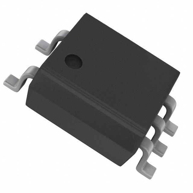
HIGH CMR, 15 Mbps OPEN COLLECTOR OUTPUT TYPE
5-PIN SOP (SO-5) 3.3 V PHOTOCOUPLER
DESCRIPTION
The PS9121 is an optically coupled high-speed, active low type isolator containing an AlGaAs LED on the
input side and a photodiode and a signal processing circuit on the output side on one chip.
The PS9121 is designed specifically for high common mode transient immunity (CMR) and low pulse width
distortion. The PS9121 is suitable for high density application.
.
FEATURES
•
•
•
•
•
•
•
•
•
•
Low power consumption (VCC = 3.3 V)
Pulse width distortion (tPHL − tPLH = 35 ns MAX.)
High common mode transient immunity (CMH, CML = ±15 kV/µs MIN.)
Small package (SO-5)
High-speed (15 Mbps)
High isolation voltage (BV = 3 750 Vr.m.s.)
Open collector output
Ordering number of tape product: PS9121-F3 : 2 500 pcs/reel
Pb-Free product
Safety standards
• UL :UL1577, Single protection
• CSA :CAN/CSA-C22.2 No.62368-1, Basic insulation
• VDE :DIN EN 60747-5-5 (Option)
APPLICATIONS
• Measurement equipment
• PDP
• FA Network
PIN CONNECTION
(Top View)
5
4
3
1. Anode
2. Cathode
3. GND
4. VO
5. VCC
1
2
TRUTH TABLE
LED
Output
ON
L
OFF
H
Start of mass production
Jul.2004
R08DS0255EJ0100 Rev.1.00
Dec 1, 2021
Page 1 of 13
�PS9121 Data Sheet
PACKAGE DIMENSIONS (UNIT: mm)
3.4+0.3
−0.1
5
4
3
7.0±0.3
(4.4)
*1
0.1±0.1
2.6±0.2
+0.10
2
0.15−0.05
1
0.5±0.3
1.27
+0.10
0.25 M
0.4−0.05
*1 ( ) indicates reference dimension.
Weight: 0.08g (typ.)
PHOTOCOUPLER CONSTRUCTION
Parameter
Air Distance
MIN.
4.2 mm
Creepage Distance
Isolation Distance
4.2 mm
0.2 mm
MARKING EXAMPLE
Ni/Pd/Au PLATING
9121
N931
No. 1 pin Mark
Initial of Renesas
(Engraved mark)
Type Number
Assembly Lot
*1
R
N
9 31
Week Assembled
Year Assembled
(Last 1 Digit)
Rank Code
*1 Bar : Pb-Free
R08DS0255EJ0100 Rev.1.00
Dec 1, 2021
Page 2 of 13
�PS9121 Data Sheet
ORDERING INFORMATION
Part Number
Order Number
Solder
Plating
Specification
Packing Style
Safety Standards
Approval
PS9121
PS9121-AX
Pb-Free
20 pcs (Tape 20 pcs cut)
Standard products
PS9121-F3
PS9121-F3-AX
(Ni/Pd/Au)
Embossed Tape 2 500
pcs/reel
(UL, CSA approved)
PS9121-V
PS9121-V-AX
20 pcs (Tape 20 pcs cut)
PS9121-V-F3
PS9121-V-F3-AX
Embossed Tape 2 500
pcs/reel
UL, CSA,
DIN EN 60747-5-5
Application
Part
Number*1
PS9121
approved
Notes*: 1. For the application of the Safety Standard, following part number should be used.
ABSOLUTE MAXIMUM RATINGS (TA = 25 °C, unless otherwise specified)
Diode
Parameter
Forward Current *1
Symbol
IF
Ratings
30
Unit
mA
Detector
Reverse Voltage
Supply Voltage
VR
VCC
5
7
V
V
Output Voltage
VO
7
V
Output Current
IO
25
mA
Power Dissipation *2
PC
40
mW
Isolation Voltage *3
Operating Ambient Temperature
BV
TA
3 750
− 40 to + 85
Vr.m.s.
°C
Storage Temperature
Tstg
− 55 to + 125
°C
Notes*: 1. Reduced to 0.3 mA/°C at TA = 25 °C or more.
2. Applies to output pin VO (collector pin). Reduced to 1.5 mW/°C at TA = 65 °C or more.
3. AC voltage for 1 minute at TA = 25 °C, RH = 60 % between input and output.
Pins 1-2 shorted together, 3-5 shorted together.
RECOMMENDED OPERATING CONDITIONS
Parameter
Symbol
MIN.
Low Level Input Voltage
VFL
0
High Level Input Current
IFH
6.3
Supply Voltage
VCC
2.7
TTL (RL = 1 kΩ, loads)
N
Pull-up Resistor
RL
R08DS0255EJ0100 Rev.1.00
Dec 1, 2021
TYP.
MAX.
Unit
0.8
V
10
12.5
mA
3.3
3.6
V
5
330
4k
Ω
Page 3 of 13
�PS9121 Data Sheet
ELECTRICAL CHARACTERISTICS (TA = − 40 to +85 °C, unless otherwise specified)
Parameter
Diode
Symbol
Conditions
MIN.
TYP.*1
MAX.
Unit
1.4
1.65
1.8
V
10
µA
Forward Voltage
VF
IF = 10 mA, TA = 25 °C
Reverse Current
IR
VR = 3 V, TA = 25 °C
Terminal Capacitance
Ct
V = 0 V, f = 1 MHz, TA = 25 °C
30
IOH
VCC = VO = 3.3 V, VF = 0.8 V
1
Detector High Level Output Current
Low Level Output Voltage*3
High Level Supply Current
Low Level Supply Current
Coupled Threshold Input Current
VOL
ICCH
ICCL
IFHL
(H → L)
1
VCC = 3.3 V, IF = 5 mA, IOL = 13 mA
0.2
VCC = 5.5 V, IF = 5 mA, IOL = 13 mA
0.2*2
VCC = 3.3 V, IF = 0 mA, VO = Open
4
5
VCC = 3.3 V, IF = 10 mA, VO = Open
7
VCC = 5.5 V, IF = 10 mA, VO = Open
9*2
VCC = 3.3 V, VO = 0.8 V, RL = 350 Ω
2.5
VCC = 5 V, VO = 0.8 V, RL = 350 Ω
2.5*2
VI-O = 1 kVDC, RH = 40 to 60 %,
TA = 25 °C
Isolation Capacitance
CI-O
V = 0 V, f = 1 MHz, TA = 25 °C
Propagation Delay Time
tPHL
tPLH
Rise Time
Fall Time
Pulse Width Distortion
tr
tf
TA = 25 °C
40
VCC = 3.3 V, RL = 350 Ω, IF = 7.5 mA
20
VCC = 5 V, RL = 350 Ω, IF = 7.5 mA
20*2
5
VCC = 5 V, RL = 350 Ω, IF = 7.5 mA
5*2
VCC = 3.3 V, RL = 350 Ω, TA = 25 °C,
IF = 0 mA, VO > 2 V, VCM = 1 kV
Common Mode
CML
R08DS0255EJ0100 Rev.1.00
Dec 1, 2021
5
VCC = 5 V, RL = 350 Ω, IF = 7.5 mA
CMH
75
ns
75
35
3*2
40
15
VCC = 5 V, RL = 350 Ω, TA = 25 °C,
IF = 0 mA, VO > 2 V, VCM = 1 kV
VCC = 3.3 V, RL = 350 Ω, TA = 25 °C,
pF
*2
VCC = 3.3 V, RL = 350 Ω, IF = 7.5 mA
Common Mode
Transient Immunity at High
Level Output*5
5
100
40
VCC = 3.3 V, RL = 350 Ω, IF = 7.5 mA
Transient Immunity at Low
Level Output*5
45
VCC = 5 V, RL = 350 Ω, IF = 7.5 mA
tPSK
10
37*2
TA = 25 °C
Propagation Delay Skew
mA
100
tPHL-tPLH VCC = 3.3 V, RL = 350 Ω, IF = 7.5 mA
(PWD)*4
7
Ω
VCC = 3.3 V, RL = 350 Ω, IF = 7.5 mA
(L → H)
*4
V
0.6
VCC = 5 V, RL = 350 Ω, IF = 7.5 mA
Propagation Delay Time
0.6
1011
VCC = 3.3 V, RL = 350 Ω, IF = 7.5 mA
(H → L)*4
µA
*2
VCC = 5.5 V, IF = 0 mA, VO = Open
RI-O
80
*2
VCC = VO = 5.5 V, VF = 0.8 V
Isolation Resistance
pF
20
kV/µs
20*2
15
20
IF = 7.5 mA, VO < 0.8 V, VCM = 1 kV
VCC = 5 V, RL = 350 Ω, TA = 25 °C,
IF = 7.5 mA, VO < 0.8 V, VCM = 1 kV
20*2
Page 4 of 13
�PS9121 Data Sheet
Notes*: 1. Typical values at TA = 25 °C.
2. These values are reference values
3. Because VOL of 2 V or more may be output when LED current input and when output supply of VCC = 2.6 V or
less, it is important to confirm the characteristics (operation with the power supply on and off) during design,
before using this device.
4. Test circuit for propagation delay time
(IF = 7.5 mA)
50%
IF
VCC = 3.3 V
Pulse Input (IF)
0.1 μF
(PW = 1 μs,
Duty cycle = 1/10)
IF Monitor
RL = 350 Ω
CL = 15 pF
VO
47 Ω
VO
tPHL
tPLH
1.5 V
VOL
Remark: CL includes probe and stray wiring capacitance.
5. Test circuit for common mode transient immunity
SW
IF
VCC = 3.3 V
0.1 μF
RL = 350 Ω
1 kV
VCM 90%
10%
VO
CL = 15 pF
0V
tr
VO
(IF = 0 mA)
VCM
VO
(IF = 7.5 mA)
tf
VOH
2V
0.8 V
VOL
Remark: CL includes probe and stray wiring capacitance.
USAGE CAUTIONS
1. This product is weak for static electricity by designed with high-speed integrated circuit so protect against
static electricity when handling.
2. By-pass capacitor of 0.1 µF is used between VCC and GND near device. Also, ensure that the distance
between the leads of the photocoupler and capacitor is no more than 10 mm.
3. Avoid storage at a high temperature and high humidity.
4. Avoid cleaning with Freon based or halogen-based (chlorinated etc.) solvents.
5. Do not use fixing agents or coatings containing halogen-based substances.
R08DS0255EJ0100 Rev.1.00
Dec 1, 2021
Page 5 of 13
�PS9121 Data Sheet
TYPICAL CHARACTERISTICS (TA = 25 °C unless otherwise specified)
DETECTOR POWER DISSIPATION
vs. AMBIENT TEMPERATURE
MAXIMUM FORWARD CURRENT
vs. AMBIENT TEMPERATURE
50
Detector Power Dissipation PC (mW)
Maximum Forward Current IF (mA)
40
30
20
10
0
20
40
80 85
60
40
30
20
10
20
100
12
High Level Supply Current ICCH (mA)
Low Level Supply Current ICCL (mA)
Forward Current IF (mA)
100
10
TA = +85°C
+50°C
+25°C
0°C
−25°C
1
0.1
1.2
1.4
1.6
1.8
2.0
2.2
10
8
ICCL (VCC = 3.3 V, IF = 10 mA)
6
ICCH (VCC = 3.3 V, IF = 0 mA)
4
2
0
−50
2.4
Forward Voltage VF (V)
−25
0
25
50
75
100
Ambient Temperature TA (°C)
LOW LEVEL OUTPUT VOLTAGE vs.
AMBIENT TEMPERATURE
OUTPUT VOLTAGE vs. INPUT CURRENT
3.5
0.6
Low Level Output Voltage VOL (V)
VCC = 3.3 V
3
Output Voltage VO (V)
100
SUPPLY CURRENT vs.
AMBIENT TEMPERATURE
FORWARD CURRENT vs.
FORWARD VOLTAGE
RL = 350 Ω
1.0 kΩ
2.5
2
4.0 kΩ, 4.7 kΩ
1.5
1
0.5
0
80 85
60
Ambient Temperature TA (°C)
Ambient Temperature TA (°C)
0.01
1.0
40
1
2
3
4
5
6
Input Current IF (mA)
IF = 5.0 mA,
VCC = 3.3 V
0.5
0.4
IOL = 16.0 mA
13.0 mA
10.0 mA
6.0 mA
0.3
0.2
0.1
0
−50
−25
0
25
50
75
100
Ambient Temperature TA (°C)
Remark The graphs indicate nominal characteristics.
R08DS0255EJ0100 Rev.1.00
Dec 1, 2021
Page 6 of 13
�PS9121 Data Sheet
THRESHOLD INPUT CURRENT vs.
AMBIENT TEMPERATURE
PROPAGATION DELAY TIME vs.
AMBIENT TEMPERATURE
4.0
3.0
RL = 350 Ω
1.0 kΩ
2.0
4.0 kΩ
1.0
0
−50
Pulse Width Distortion |tPHL− tPLH| (ns)
Propagation Delay Time tPHL, tPLH (ns)
VCC = 3.3 V,
VO = 0.6 V
−25
0
25
50
75
120
100
IF = 7.5 mA,
VCC = 3.3 V
tPLH: RL = 4.7 kΩ
tPLH: RL = 4.0 kΩ
80
tPLH: RL = 1.0 kΩ
tPLH: RL = 350 Ω
60
40
20
0
−50
100
tPHL: RL = 350 Ω, 1.0 kΩ, 4.0 kΩ, 4.7 kΩ
−25
0
25
50
75
Ambient Temperature TA (°C)
Ambient Temperature TA (°C)
PULSE WIDTH DISTORTION vs.
AMBIENT TEMPERATURE
SWITCHING TIME vs.
AMBIENT TEMPERATURE
100
300
100
IF = 7.5 mA,
VCC = 3.3 V
250
80
Switching Time tr, tf (ns)
Threshold Input Current IFHL (mA)
5.0
RL = 4.7 kΩ
60
RL = 4.0 kΩ
40
RL = 1.0 kΩ
RL = 350 Ω
20
0
−50
−25
0
25
IF = 7.5 mA,
VCC = 3.3 V
200
150
tr: RL = 1.0 kΩ
tr: RL = 350 Ω
tf: RL = 350 Ω, 1.0 kΩ, 4.0 kΩ, 4.7 kΩ
100
50
50
75
100
Ambient Temperature TA (°C)
tr: RL = 4.7 kΩ
tr: RL = 4.0 kΩ
0
−50
−25
0
25
50
75
100
Ambient Temperature TA (°C)
Propagation Delay Time tPHL, tPLH (ns)
PROPAGATION DELAY TIME vs.
INPUT CURRENT
120
tPLH: RL = 4.7 kΩ
VCC = 3.3 V
100
tPLH: RL = 4.0 kΩ
80
tPLH: RL = 1.0 kΩ
tPLH: RL = 350 Ω
60
40
20
0
5
tPHL: RL = 350 Ω, 1.0 kΩ, 4.0 kΩ, 4.7 kΩ
7
9
11
13
15
Input Current IF (mA)
Remark The graphs indicate nominal characteristics.
R08DS0255EJ0100 Rev.1.00
Dec 1, 2021
Page 7 of 13
�PS9121 Data Sheet
TAPING SPECIFICATIONS (UNIT: mm)
Tape Direction
5 pin SOP (F3)
⌀1.55±0.1
3.9±0.1
8.0±0.1
7.4±0.1
5.5±0.1
⌀1.5+0.1
−0
12.0±0.2
2.0±0.05
4.0±0.1
1.75±0.1
Outline and Dimensions (Tape)
3.45 MAX.
3.0±0.1
0.3±0.05
Outline and Dimensions (Reel)
2.0±0.5
R1.0
⌀21.0±0.8
⌀100±1.0
⌀13.0±0.2
⌀330±2.0
2.0±0.5
13.5±1.0
17.5±1.0
Packing: 2 500 pcs/reel
R08DS0255EJ0100 Rev.1.00
Dec 1, 2021
Page 8 of 13
�PS9121 Data Sheet
RECOMMENDED MOUNT PAD DIMENSIONS (UNIT: mm)
1.27
2.54
0.8
1.45
6.25
Remark
All dimensions in this figure must be evaluated before use.
R08DS0255EJ0100 Rev.1.00
Dec 1, 2021
Page 9 of 13
�PS9121 Data Sheet
NOTES ON HANDLING
1. Recommended soldering conditions
(1) Infrared reflow soldering
• Peak reflow temperature
• Time of peak reflow temperature
• Time of temperature higher than 220 °C
• Time to preheat temperature from 120 to 180 °C
• Number of reflows
• Flux
260 °C or below (package surface temperature)
10 seconds or less
60 seconds or less
120 ± 30 s
Three
Rosin flux containing small amount of chlorine
(The flux with a maximum chlorine content of
0.2 Wt% is recommended.)
Package Surface Temperature T (°C)
Recommended Temperature Profile of Infrared Reflow
(heating)
to 10 s
260°C MAX.
220°C
to 60 s
180°C
120°C
120±30 s
(preheating)
Time (s)
(2) Wave soldering
• Temperature
• Time
• Preheating conditions
• Number of times
• Flux
260 °C or below (molten solder temperature)
10 seconds or less
120 °C or below (package surface temperature)
One (Allowed to be dipped in solder including plastic mold portion.)
Rosin flux containing small amount of chlorine (The flux with a maximum
chlorine content of 0.2 Wt% is recommended.)
(3) Soldering by Soldering Iron
• Peak Temperature (lead part temperature) 350 °C or below
• Time (each pins)
3 seconds or less
• Flux
Rosin flux containing small amount of chlorine
(The flux with a maximum chlorine content of 0.2 Wt% is recommended.)
(a) Soldering of leads should be made at the point 1.5 to 2.0 mm from the root of the lead
(b) Please be sure that the temperature of the package would not be heated over 100 °C
(4) Cautions
• Flux Cleaning
Avoid cleaning with Freon based or halogen-based (chlorinated etc.) solvents.
• Do not use fixing agents or coatings containing halogen-based substances.
2. Cautions regarding noise
Be aware that when voltage is applied suddenly between the photocoupler’s input and output or between
collector-emitters at startup, the output transistor may enter the on state, even if the voltage is within the
absolute maximum ratings.
R08DS0255EJ0100 Rev.1.00
Dec 1, 2021
Page 10 of 13
�PS9121 Data Sheet
SPECIFICATION OF VDE MARKS LICENSE DOCUMENT
Parameter
Symbol
Climatic test class (IEC 60068-1/DIN EN 60068-1)
Rating
Unit
40/85/21
Dielectric strength
maximum operating isolation voltage
Test voltage (partial discharge test, procedure a for type test and random test)
Upr = 1.6 × UIORM., Pd < 5 pC
UIORM
Upr
707
1 131
Vpeak
Vpeak
Upr
1 326
Vpeak
UIOTM
6 000
Vpeak
Test voltage (partial discharge test, procedure b for all devices)
Upr = 1.875 × UIORM., Pd < 5 pC
Highest permissible overvoltage
Degree of pollution (IEC 60664-1/DIN EN 60664-1 (VDE 0110-1))
2
Comparative tracking index (IEC 60112/DIN EN 60112 (VDE 0303-11))
CTI
Material group (IEC 60664-1/DIN EN 60664-1 (VDE 0110-1))
175
III a
Storage temperature range
Tstg
− 55 to +125
°C
Operating temperature range
TA
− 40 to +85
°C
Ris MIN.
Ris MIN.
1012
1011
Ω
Ω
Tsi
Isi
Psi
150
200
300
°C
mA
mW
Ris MIN.
109
Ω
Isolation resistance, minimum value
VIO = 500 V dc at TA = 25 °C
VIO = 500 V dc at TA MAX. at least 100 °C
Safety maximum ratings (maximum permissible in case of fault, see thermal
derating curve)
Package temperature
Current (input current IF, Psi = 0)
Power (output or total power dissipation)
Isolation resistance
VIO = 500 V dc at TA = Tsi
Dependence of maximum safety ratings with package temperature
Total Power Dissipation Psi (mW)
Input Current Isi (mA)
1000
900
800
700
600
500
400
Psi: Total Power Dissipation
300
200
100
Isi: Input Current
0
0
25
50
75
100
125
150
175
200
Package temp Tsi (°C)
R08DS0255EJ0100 Rev.1.00
Dec 1, 2021
Page 11 of 13
�PS9121 Data Sheet
Method a) Destructive Test, Type and Sample Test
UIOTM = 6000 V
V
Upr = 1131 V
UIORM = 707 V
t3
t1
tini
t2
tm
t4
t
ttest
t1, t2 = 1 to 10 sec
t3, t4 = 1 sec
tm(PARTIAL DISCHARGE) = 10 sec
ttest = 12 sec
tini = 60 sec
Method b) Non-destructive Test, 100% Production Test
Upr = 1326 V
V
UIORM = 707 V
ttest
t3
tm
t
t4
t3, t4 = 0.1 sec
tm(PARTIAL DISCHARGE) = 1.0 sec
ttest = 1.2 sec
R08DS0255EJ0100 Rev.1.00
Dec 1, 2021
Page 12 of 13
�PS9121 Data Sheet
Caution
GaAs Products
This product uses gallium arsenide (GaAs).
GaAs vapor and powder are hazardous to human health if inhaled or ingested, so please observe
the following points.
• Follow related laws and ordinances when disposing of the product. If there are no applicable laws
and/or ordinances, dispose of the product as recommended below.
1. Commission a disposal company able to (with a license to) collect, transport and dispose of
materials that contain arsenic and other such industrial waste materials.
2. Exclude the product from general industrial waste and household garbage, and ensure that the
product is controlled (as industrial waste subject to special control) up until final disposal.
• Do not burn, destroy, cut, crush, or chemically dissolve the product.
• Do not lick the product or i any way allow it to enter the mouth.
All trademarks and registered trademarks are the property of their respective owners.
R08DS0255EJ0100 Rev.1.00
Dec 1, 2021
Page 13 of 13
�Notice
1.
2.
3.
4.
5.
6.
7.
8.
9.
10.
11.
12.
13.
14.
Descriptions of circuits, software and other related information in this document are provided only to illustrate the operation of semiconductor products
and application examples. You are fully responsible for the incorporation or any other use of the circuits, software, and information in the design of your
product or system. Renesas Electronics disclaims any and all liability for any losses and damages incurred by you or third parties arising from the use
of these circuits, software, or information.
Renesas Electronics hereby expressly disclaims any warranties against and liability for infringement or any other claims involving patents, copyrights,
or other intellectual property rights of third parties, by or arising from the use of Renesas Electronics products or technical information described in this
document, including but not limited to, the product data, drawings, charts, programs, algorithms, and application examples.
No license, express, implied or otherwise, is granted hereby under any patents, copyrights or other intellectual property rights of Renesas Electronics
or others.
You shall be responsible for determining what licenses are required from any third parties, and obtaining such licenses for the lawful import, export,
manufacture, sales, utilization, distribution or other disposal of any products incorporating Renesas Electronics products, if required.
You shall not alter, modify, copy, or reverse engineer any Renesas Electronics product, whether in whole or in part. Renesas Electronics disclaims any
and all liability for any losses or damages incurred by you or third parties arising from such alteration, modification, copying or reverse engineering.
Renesas Electronics products are classified according to the following two quality grades: “Standard” and “High Quality”. The intended applications for
each Renesas Electronics product depends on the product’s quality grade, as indicated below.
"Standard": Computers; office equipment; communications equipment; test and measurement equipment; audio and visual equipment; home
electronic appliances; machine tools; personal electronic equipment; industrial robots; etc.
"High Quality": Transportation equipment (automobiles, trains, ships, etc.); traffic control (traffic lights); large-scale communication equipment; key
financial terminal systems; safety control equipment; etc.
Unless expressly designated as a high reliability product or a product for harsh environments in a Renesas Electronics data sheet or other Renesas
Electronics document, Renesas Electronics products are not intended or authorized for use in products or systems that may pose a direct threat to
human life or bodily injury (artificial life support devices or systems; surgical implantations; etc.), or may cause serious property damage (space
system; undersea repeaters; nuclear power control systems; aircraft control systems; key plant systems; military equipment; etc.). Renesas Electronics
disclaims any and all liability for any damages or losses incurred by you or any third parties arising from the use of any Renesas Electronics product
that is inconsistent with any Renesas Electronics data sheet, user’s manual or other Renesas Electronics document.
No semiconductor product is absolutely secure. Notwithstanding any security measures or features that may be implemented in Renesas Electronics
hardware or software products, Renesas Electronics shall have absolutely no liability arising out of any vulnerability or security breach, including but
not limited to any unauthorized access to or use of a Renesas Electronics product or a system that uses a Renesas Electronics product. RENESAS
ELECTRONICS DOES NOT WARRANT OR GUARANTEE THAT RENESAS ELECTRONICS PRODUCTS, OR ANY SYSTEMS CREATED USING
RENESAS ELECTRONICS PRODUCTS WILL BE INVULNERABLE OR FREE FROM CORRUPTION, ATTACK, VIRUSES, INTERFERENCE,
HACKING, DATA LOSS OR THEFT, OR OTHER SECURITY INTRUSION (“Vulnerability Issues”). RENESAS ELECTRONICS DISCLAIMS ANY AND
ALL RESPONSIBILITY OR LIABILITY ARISING FROM OR RELATED TO ANY VULNERABILITY ISSUES. FURTHERMORE, TO THE EXTENT
PERMITTED BY APPLICABLE LAW, RENESAS ELECTRONICS DISCLAIMS ANY AND ALL WARRANTIES, EXPRESS OR IMPLIED, WITH
RESPECT TO THIS DOCUMENT AND ANY RELATED OR ACCOMPANYING SOFTWARE OR HARDWARE, INCLUDING BUT NOT LIMITED TO
THE IMPLIED WARRANTIES OF MERCHANTABILITY, OR FITNESS FOR A PARTICULAR PURPOSE.
When using Renesas Electronics products, refer to the latest product information (data sheets, user’s manuals, application notes, “General Notes for
Handling and Using Semiconductor Devices” in the reliability handbook, etc.), and ensure that usage conditions are within the ranges specified by
Renesas Electronics with respect to maximum ratings, operating power supply voltage range, heat dissipation characteristics, installation, etc. Renesas
Electronics disclaims any and all liability for any malfunctions, failure or accident arising out of the use of Renesas Electronics products outside of such
specified ranges.
Although Renesas Electronics endeavors to improve the quality and reliability of Renesas Electronics products, semiconductor products have specific
characteristics, such as the occurrence of failure at a certain rate and malfunctions under certain use conditions. Unless designated as a high reliability
product or a product for harsh environments in a Renesas Electronics data sheet or other Renesas Electronics document, Renesas Electronics
products are not subject to radiation resistance design. You are responsible for implementing safety measures to guard against the possibility of bodily
injury, injury or damage caused by fire, and/or danger to the public in the event of a failure or malfunction of Renesas Electronics products, such as
safety design for hardware and software, including but not limited to redundancy, fire control and malfunction prevention, appropriate treatment for
aging degradation or any other appropriate measures. Because the evaluation of microcomputer software alone is very difficult and impractical, you are
responsible for evaluating the safety of the final products or systems manufactured by you.
Please contact a Renesas Electronics sales office for details as to environmental matters such as the environmental compatibility of each Renesas
Electronics product. You are responsible for carefully and sufficiently investigating applicable laws and regulations that regulate the inclusion or use of
controlled substances, including without limitation, the EU RoHS Directive, and using Renesas Electronics products in compliance with all these
applicable laws and regulations. Renesas Electronics disclaims any and all liability for damages or losses occurring as a result of your noncompliance
with applicable laws and regulations.
Renesas Electronics products and technologies shall not be used for or incorporated into any products or systems whose manufacture, use, or sale is
prohibited under any applicable domestic or foreign laws or regulations. You shall comply with any applicable export control laws and regulations
promulgated and administered by the governments of any countries asserting jurisdiction over the parties or transactions.
It is the responsibility of the buyer or distributor of Renesas Electronics products, or any other party who distributes, disposes of, or otherwise sells or
transfers the product to a third party, to notify such third party in advance of the contents and conditions set forth in this document.
This document shall not be reprinted, reproduced or duplicated in any form, in whole or in part, without prior written consent of Renesas Electronics.
Please contact a Renesas Electronics sales office if you have any questions regarding the information contained in this document or Renesas
Electronics products.
(Note1)
(Note2)
“Renesas Electronics” as used in this document means Renesas Electronics Corporation and also includes its directly or indirectly controlled
subsidiaries.
“Renesas Electronics product(s)” means any product developed or manufactured by or for Renesas Electronics.
(Rev.5.0-1 October 2020)
Corporate Headquarters
Contact information
TOYOSU FORESIA, 3-2-24 Toyosu,
Koto-ku, Tokyo 135-0061, Japan
For further information on a product, technology, the most up-to-date
version of a document, or your nearest sales office, please visit:
www.renesas.com/contact/.
www.renesas.com
Trademarks
Renesas and the Renesas logo are trademarks of Renesas Electronics
Corporation. All trademarks and registered trademarks are the property
of their respective owners.
© 2021 Renesas Electronics Corporation. All rights reserved.
�