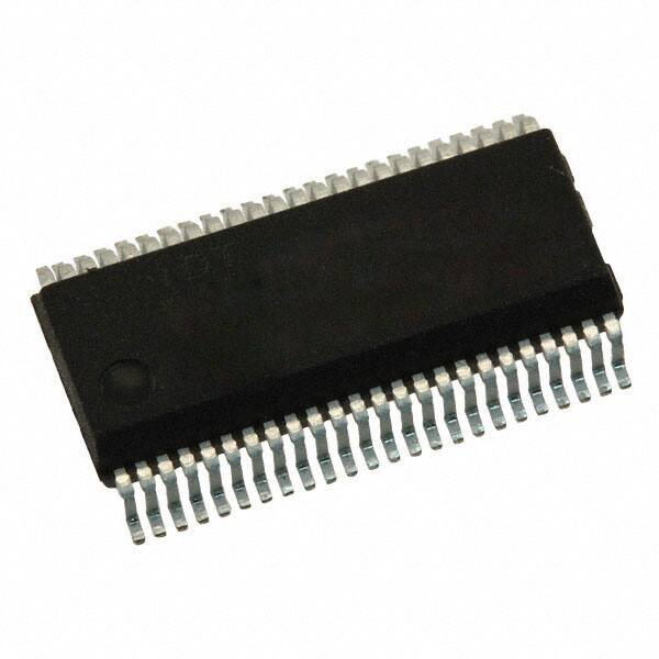
IDTQS4A215
HIGH-PERFORMANCE CMOS SIX-CHANNEL SP4T MUX/DEMUX
INDUSTRIAL TEMPERATURE RANGE
QUICKSWITCH® PRODUCTS
HIGH-PERFORMANCE CMOS
SIX CHANNEL SP4T MUX/DEMUX
FEATURES:
•
•
•
•
•
•
•
•
•
•
DESCRIPTION:
Ω
Low ON resistance: r DS(ON) = 5Ω
Fast transition time: t TRAN = 6ns
Wide bandwidth: 700MHz (-3dB point)
Crosstalk: -110dB at 50KHz, -68dB at 5MHz, -66dB at 30MHz
Off-isolation: -90dB at 50KHz, -60dB at 5MHz, -50dB at 30MHz
Single 5V supply
Can be used as multiplexer or demultiplexer
TTL-compatible control inputs
μA
Ultra-low quiescent current: 9μ
Available in QVSOP package
The QS4A215 is a high-performance CMOS six-channel multiplexer/
demultiplexer with individual enables. The low ON-resistance of the QS4A215
allows inputs to be connected to outputs with low insertion loss and high
bandwidth. TTL-compatible control circuitry with “Break-Before-Make”
feature prevents contention.
The QS4A215 with 700MHz bandwidth makes it ideal for high-performance video signal switching, audio signal switching, and telecom routing
applications. High performance and low power dissipation makes this
device ideal for battery operated and remote instrumentation applications.
The QS4A215 is offered in the QVSOP package which has several
advantages over conventional packages such as PDIP and SOIC, including:
• Reduced signal delays due to denser component packaging on circuit
boards
• Reduced system noise due to less pin inductance, resulting in lower
ground bounce
APPLICATIONS:
•
•
•
•
•
•
•
•
•
IDTQS4A215
High-speed video signal switching/routing
HDTV-quality video signal multiplexing
Audio signal switching/routing
Data acquisition
ATE systems
Telecomm routing
Switch between multiple video sources
Token Ring transceivers
High-speed networking
The QS4A215 is characterized for operation at -40°C to +85°C.
FUNCTIONAL BLOCK DIAGRAM
I0A
I0C
I1A
I1C
YA
YC
I2A
I2C
I3A
I3C
I0B
I0D
I1B
I1D
YB
I2D
I3B
I3D
S1AB
EA
EB
S1 C D
EC
YE
I3E
I0F
I1F
YF
I2F
I3F
S0 C D
CO NTRO L
LOG IC
I1E
I2E
YD
I2B
S0AB
I0E
S0 E F
CO NTRO L
LOG IC
ED
S1 E F
EE
CO NTRO L
LOG IC
EF
IDT and the IDT logo are registered trademarks of Integrated Device Technology, Inc.
INDUSTRIAL TEMPERATURE RANGE
JULY 2015
1
c 2015 Integrated Device Technology, Inc.
DSC-5549/5
�IDTQS4A215
HIGH-PERFORMANCE CMOS SIX-CHANNEL SP4T MUX/DEMUX
INDUSTRIAL TEMPERATURE RANGE
ABSOLUTE MAXIMUM RATINGS(1)
PIN CONFIGURATION
EA
1
48
VCC
S1AB
2
47
EB
I3A
3
46
S0AB
Symbol
Description
VTERM(2)
Max
Unit
VTERM(3)
Supply Voltage to Ground
–0.5 to +7
V
DC Switch Voltage VS
–0.5 to +7
V
—
Analog Input Voltage
–0.5 to +7
V
VTERM(3)
DC Input Voltage VIN
–0.5 to +7
V
VAC
AC Input Voltage (pulse width ≤20ns)
–3
V
IOUT
DC Output Current
120
mA
PMAX
Maximum Power Dissipation
0.7
W
TSTG
Storage Temperature
–65 to +150
°C
I2A
4
45
I3B
I1A
5
44
I2B
I0A
6
43
I1B
YA
7
42
I0B
GND
8
41
YB
EC
9
40
VCC
S1CD
10
39
ED
I3C
11
38
S0CD
I2C
12
37
I3D
I1C
13
36
I2D
Pin Names
I/O
I0C
14
35
I1D
Ixx
I/O
I
NOTES:
1. Stresses greater than those listed under ABSOLUTE MAXIMUM RATINGS may cause
permanent damage to the device. This is a stress rating only and functional operation
of the device at these or any other conditions above those indicated in the operational
sections of this specification is not implied. Exposure to absolute maximum rating
conditions for extended periods may affect reliability.
2. VCC terminals.
3. All terminals except VCC .
PIN DESCRIPTION
YC
15
34
I0D
S0XX, S1XX
Ex
I
GND
16
33
YD
Yx
I/O
EE
17
32
VCC
S1EF
18
31
EF
I3E
19
30
S0EF
I2E
20
29
I3F
I1E
21
28
I2F
Description
Demux Ports A-F
Select Inputs
Enable Inputs A-F
Mux Ports A-F
FUNCTION TABLE(1)
Enable
Select
Mux/Demux
Ports
EA
EB
S1
S0
YA
YB
Function
H
X
X
X
Z
X
Disable A
I0E
22
27
I1F
YE
23
26
I0F
X
H
X
X
X
Z
Disable B
GND
24
25
YF
L
L
L
L
I0A
I0 B
S1AB, S0AB = 0
L
L
L
H
I1A
I1 B
S1AB, S0AB = 1
L
L
H
L
I2A
I2 B
S1AB, S0AB = 2
L
L
H
H
I3A
I3 B
S1AB, S0AB = 3
QVSOP
TOP VIEW
NOTE:
1. H = HIGH Voltage Level
L = LOW Voltage Level
X = Don't Care
Z = High-Impedance
2. This function table represents the function for block “AB”. The “CD” block
nomenclature substitutes “A” for “C” and “B” for “D”. The “EF” block nomenclature
substitutes “A” for “E” and “B” for “F”.
2
�IDTQS4A215
HIGH-PERFORMANCE CMOS SIX-CHANNEL SP4T MUX/DEMUX
INDUSTRIAL TEMPERATURE RANGE
DC ELECTRICAL CHARACTERISTICS OVER OPERATING RANGE
Following Conditions Apply Unless Otherwise Specified:
Industrial: TA = –40°C to +85°C, VCC = 5V ± 5%
Symbol
Parameter
Test Conditions
Min.
Typ.(1) Max.
Unit
Analog Switch
VIN
Analog Signal Range(2)
–0.5
1
Vcc - 1
V
—
5
7
Ω
rDS(ON)
Drain-source ON resistance(2,3)
Vcc = Min., VIN = 0V, ION = 30mA
Vcc = Min., VIN = 2.4V, ION = 15mA
—
13
17
IC(OFF)
Channel Off Leakage Current
IN = Vcc or 0V; YN = 0V or Vcc; EX = Vcc
—
10
—
nA
IC(ON)
Channel On Leakage Current
IN = YN = 0V
—
10
—
nA
(each channel is turned on sequentially)
Digital Control
VIH
Input HIGH Voltage
Guaranteed Logic HIGH for Control Pins
2
—
—
V
VIL
Input LOW Voltage
Guaranteed Logic LOW for Control Pins
—
—
0.8
V
Switching Time of Mux
RL = 1KΩ, CL = 100pF
0.5
—
6.6
ns
Sx to Yx
(See Transition Time)
0.5
—
6
ns
0.5
—
6
ns
Dynamic Characteristics
tTRANS
tON(EN)
tOFF(EN)
Enable Turn-On Time
RL = 1KΩ, CL = 100pF
EX to Yx
(See Switching Time)
Enable Turn-Off Time
RL = 1KΩ, CL = 100pF
EX to Yx
(See Switching Time)
tPD
Group Delay(2,4)
RL = 1KΩ, CL = 100pF
—
—
250
ps
f3dB
-3dB Bandwidth
VIN = 1Vp-p, RL = 75Ω
—
700
—
MHz
Off-isolation
VIN = 1Vp-p, RL = 75Ω, f = 5MHz
—
-60
—
dB
Crosstalk
VIN = 1Vp-p, RL = 75Ω, f = 5MHz
—
-68
—
dB
Mux Off Capacitance
EX = Vcc, VIN = VOUT = 0V
—
6
—
pF
Demux Off Capacitance
EX = Vcc, VIN = VOUT = 0V
—
14
—
pF
Mux On Capacitance
EX = 0V, VIN = VOUT = 0V
—
20
—
pF
Demux On Capacitance
EX = 0V, VIN = VOUT = 0V
—
20
—
pF
Charge Injection
CL = 1000pF
—
1.5
—
pC
XTALK
CMUX(OFF)
CDEMUX(OFF)
CMUX(ON)
CDEMUX(ON)
QCI
NOTES:
1. Typical values are at VCC = 5.0V, TA = 25°C.
2. Max value is guaranteed but not production tested.
3. Measured by voltage drop between A and C pins or B and D pins at indicated current through the switch. ON resistance is determined by the lower of the voltages on the
two (I, Y) pins.
4. The bus switch contributes no group delay other than the RC delay of the ON resistance of the switch and load capacitance. Group delay of the bus switch, when used
in a system, is determined by the driving circuit on the driving side of the switch and its interaction with the load on the driven side.
POWER SUPPLY CHARACTERISTICS
Symbol
ICCQ
Parameter
Quiescent Power
Test Conditions
VCC = Max., VIN = GND or VCC, f = 0
3
Max.
Unit
9
μA
�IDTQS4A215
HIGH-PERFORMANCE CMOS SIX-CHANNEL SP4T MUX/DEMUX
INDUSTRIAL TEMPERATURE RANGE
TYPICAL CHARACTERISTICS
60
150
V CC = 5V
R L = 75
120
V CC = 5V
R L = 75
50
40
(dB )
90
Crosstalk
Crosstalk
30
(dB )
O ff-isolation
60
O ff-isolation
20
30
10
0
1K
10K
100K
1M
10M
100M
1G
0
100M
Frequency (H z)
200M
300M
400M
500M
600M
700M
Frequency (H z)
Off-isolation and Crosstalk vs. Frequency
Off-isolation and Crosstalk vs. Frequency
NOTES:
1. Crosstalk = 20 log |VO/VS|
2. Off-isolation = 20 log |VO/VS|
NOTES:
1. Crosstalk = 20 log |VO/VS|
2. Off-isolation = 20 log |VO/VS|
160
140
4
V CC = 5V
R L = 75
Crosstalk
2
R L = 1K
120
(dB )
(dB )
0
100
R L = 75
V CC = 5V
2
Off-isolation
80
4
60
6
1K
40
10K
20K
30K
40K
50K
60K
70K
10K
100K
1M
10M
Frequency (H z)
Frequency (H z)
Insertion Loss vs. Frequency
Off-isolation and Crosstalk vs. Frequency
NOTE:
1. Insertion Loss = 20 log |VO/VS|
NOTES:
1. Crosstalk = 20 log |VO/VS|
2. Off-isolation = 20 log |VO/VS|
4
100M
1G
�IDTQS4A215
HIGH-PERFORMANCE CMOS SIX-CHANNEL SP4T MUX/DEMUX
INDUSTRIAL TEMPERATURE RANGE
TYPICAL CHARACTERISTICS (CONTINUED)
18
2
R L = 1K
16
r DS (On) - Drain Source On-resistance( )
1
(dB )
0
1
R L = 75
V CC = 5V
2
4
6
100M
200M
400M
300M
500M
600M
700M
Frequency (H z)
14
12
VCC = 4.75V
10
8
6
4
Insertion Loss vs. Frequency
0.0
0.5
1.0
1.5
2.0
2.5
3.0
VIN (Volts)
NOTE:
1. Insertion Loss = 20 log |VO/VS|
RON LINK
On-Resistance vs. VIN
TEST CIRCUITS
5V
3.0V
VCC
0V
SELECT
INPUT
I0A-I2A
EA
I3A
S0
0V
5V
QS4A215
tTRANS
I0B-I3B
VIN
1.5V
tTRANS
S1
YB
5V
50
SWITCH
OUTPUT
VOUT
EB
GND
YA
500
50pF
Transition Time
5
1.5V
�IDTQS4A215
HIGH-PERFORMANCE CMOS SIX-CHANNEL SP4T MUX/DEMUX
INDUSTRIAL TEMPERATURE RANGE
TEST CIRCUITS (CONTINUED)
5V
3.0V
CONTROL
INPUT
1.5V
I1A-I3A
VCC
0V
S0
tON(EN)
5V
I0A
QS4A215
S1
I0B-I3B
EB
5V
OUTPUT
0.3V
OUTPUT
0.3V
YB
VIN
EA
VOUT
YA
GND
500
50
50pF
tOFF(EN)
Enable Switching Time
+5V
VS
+5V
VIN
VCC
I0A
VCC
I0A
IxA
RS = 50
YO
QS4A215
S1
EB
RS = 50
GND
Insertion Loss
NOTE:
1. Crosstalk = 20 log |VO/VS|
+5V
VCC
IxA
QS4A215
S1
YO
YA
RL
75
S0
EA
EB
EA
EB
Crosstalk
NOTE:
1. Insertion Loss = 20 log |VO/VS|
IxB
RL
75
S0
S1
RS = 50
YA
IxB
RL
75
EA
YO
QS4A215
YA
S0
GND
+5V
Off-Isolation
NOTE:
1. Off-isolation = 20 log |VO/VS|
6
GND
�IDTQS4A215
HIGH-PERFORMANCE CMOS SIX-CHANNEL SP4T MUX/DEMUX
INDUSTRIAL TEMPERATURE RANGE
ORDERING INFORMATION
QS
XXXXX
XX
Device Type Package
X
Blank
8
Tube or Tray
Tape and Reel
Q1G
QVSOP - Green
4A215
High Performance CMOS Six Channel SP4T
MUX/DEMUX
DATASHEET DOCUMENT HISTORY
04/13/2014
Pg. 7
07/07/2015
Pg. 1,7
Updated the Ordering Information by removing non green package version, the "IDT" notation and Adding Tape
and Reel information.
Updated the Ordering Information from QG to Q1G accordingly.
7
�IMPORTANT NOTICE AND DISCLAIMER
RENESAS ELECTRONICS CORPORATION AND ITS SUBSIDIARIES (“RENESAS”) PROVIDES TECHNICAL
SPECIFICATIONS AND RELIABILITY DATA (INCLUDING DATASHEETS), DESIGN RESOURCES (INCLUDING
REFERENCE DESIGNS), APPLICATION OR OTHER DESIGN ADVICE, WEB TOOLS, SAFETY INFORMATION, AND
OTHER RESOURCES “AS IS” AND WITH ALL FAULTS, AND DISCLAIMS ALL WARRANTIES, EXPRESS OR IMPLIED,
INCLUDING, WITHOUT LIMITATION, ANY IMPLIED WARRANTIES OF MERCHANTABILITY, FITNESS FOR A
PARTICULAR PURPOSE, OR NON-INFRINGEMENT OF THIRD PARTY INTELLECTUAL PROPERTY RIGHTS.
These resources are intended for developers skilled in the art designing with Renesas products. You are solely responsible
for (1) selecting the appropriate products for your application, (2) designing, validating, and testing your application, and (3)
ensuring your application meets applicable standards, and any other safety, security, or other requirements. These
resources are subject to change without notice. Renesas grants you permission to use these resources only for
development of an application that uses Renesas products. Other reproduction or use of these resources is strictly
prohibited. No license is granted to any other Renesas intellectual property or to any third party intellectual property.
Renesas disclaims responsibility for, and you will fully indemnify Renesas and its representatives against, any claims,
damages, costs, losses, or liabilities arising out of your use of these resources. Renesas' products are provided only subject
to Renesas' Terms and Conditions of Sale or other applicable terms agreed to in writing. No use of any Renesas resources
expands or otherwise alters any applicable warranties or warranty disclaimers for these products.
(Rev.1.0 Mar 2020)
Corporate Headquarters
Contact Information
TOYOSU FORESIA, 3-2-24 Toyosu,
Koto-ku, Tokyo 135-0061, Japan
www.renesas.com
For further information on a product, technology, the most
up-to-date version of a document, or your nearest sales
office, please visit:
www.renesas.com/contact/
Trademarks
Renesas and the Renesas logo are trademarks of Renesas
Electronics Corporation. All trademarks and registered
trademarks are the property of their respective owners.
© 2020 Renesas Electronics Corporation. All rights reserved.
�