To our customers,
Old Company Name in Catalogs and Other Documents
On April 1st, 2010, NEC Electronics Corporation merged with Renesas Technology
Corporation, and Renesas Electronics Corporation took over all the business of both
companies. Therefore, although the old company name remains in this document, it is a valid
Renesas Electronics document. We appreciate your understanding.
Renesas Electronics website: http://www.renesas.com
April 1st, 2010
Renesas Electronics Corporation
Issued by: Renesas Electronics Corporation (http://www.renesas.com)
Send any inquiries to http://www.renesas.com/inquiry.
�Notice
1.
2.
3.
4.
5.
6.
7.
All information included in this document is current as of the date this document is issued. Such information, however, is
subject to change without any prior notice. Before purchasing or using any Renesas Electronics products listed herein, please
confirm the latest product information with a Renesas Electronics sales office. Also, please pay regular and careful attention to
additional and different information to be disclosed by Renesas Electronics such as that disclosed through our website.
Renesas Electronics does not assume any liability for infringement of patents, copyrights, or other intellectual property rights
of third parties by or arising from the use of Renesas Electronics products or technical information described in this document.
No license, express, implied or otherwise, is granted hereby under any patents, copyrights or other intellectual property rights
of Renesas Electronics or others.
You should not alter, modify, copy, or otherwise misappropriate any Renesas Electronics product, whether in whole or in part.
Descriptions of circuits, software and other related information in this document are provided only to illustrate the operation of
semiconductor products and application examples. You are fully responsible for the incorporation of these circuits, software,
and information in the design of your equipment. Renesas Electronics assumes no responsibility for any losses incurred by
you or third parties arising from the use of these circuits, software, or information.
When exporting the products or technology described in this document, you should comply with the applicable export control
laws and regulations and follow the procedures required by such laws and regulations. You should not use Renesas
Electronics products or the technology described in this document for any purpose relating to military applications or use by
the military, including but not limited to the development of weapons of mass destruction. Renesas Electronics products and
technology may not be used for or incorporated into any products or systems whose manufacture, use, or sale is prohibited
under any applicable domestic or foreign laws or regulations.
Renesas Electronics has used reasonable care in preparing the information included in this document, but Renesas Electronics
does not warrant that such information is error free. Renesas Electronics assumes no liability whatsoever for any damages
incurred by you resulting from errors in or omissions from the information included herein.
Renesas Electronics products are classified according to the following three quality grades: “Standard”, “High Quality”, and
“Specific”. The recommended applications for each Renesas Electronics product depends on the product’s quality grade, as
indicated below. You must check the quality grade of each Renesas Electronics product before using it in a particular
application. You may not use any Renesas Electronics product for any application categorized as “Specific” without the prior
written consent of Renesas Electronics. Further, you may not use any Renesas Electronics product for any application for
which it is not intended without the prior written consent of Renesas Electronics. Renesas Electronics shall not be in any way
liable for any damages or losses incurred by you or third parties arising from the use of any Renesas Electronics product for an
application categorized as “Specific” or for which the product is not intended where you have failed to obtain the prior written
consent of Renesas Electronics. The quality grade of each Renesas Electronics product is “Standard” unless otherwise
expressly specified in a Renesas Electronics data sheets or data books, etc.
“Standard”:
8.
9.
10.
11.
12.
Computers; office equipment; communications equipment; test and measurement equipment; audio and visual
equipment; home electronic appliances; machine tools; personal electronic equipment; and industrial robots.
“High Quality”: Transportation equipment (automobiles, trains, ships, etc.); traffic control systems; anti-disaster systems; anticrime systems; safety equipment; and medical equipment not specifically designed for life support.
“Specific”:
Aircraft; aerospace equipment; submersible repeaters; nuclear reactor control systems; medical equipment or
systems for life support (e.g. artificial life support devices or systems), surgical implantations, or healthcare
intervention (e.g. excision, etc.), and any other applications or purposes that pose a direct threat to human life.
You should use the Renesas Electronics products described in this document within the range specified by Renesas Electronics,
especially with respect to the maximum rating, operating supply voltage range, movement power voltage range, heat radiation
characteristics, installation and other product characteristics. Renesas Electronics shall have no liability for malfunctions or
damages arising out of the use of Renesas Electronics products beyond such specified ranges.
Although Renesas Electronics endeavors to improve the quality and reliability of its products, semiconductor products have
specific characteristics such as the occurrence of failure at a certain rate and malfunctions under certain use conditions. Further,
Renesas Electronics products are not subject to radiation resistance design. Please be sure to implement safety measures to
guard them against the possibility of physical injury, and injury or damage caused by fire in the event of the failure of a
Renesas Electronics product, such as safety design for hardware and software including but not limited to redundancy, fire
control and malfunction prevention, appropriate treatment for aging degradation or any other appropriate measures. Because
the evaluation of microcomputer software alone is very difficult, please evaluate the safety of the final products or system
manufactured by you.
Please contact a Renesas Electronics sales office for details as to environmental matters such as the environmental
compatibility of each Renesas Electronics product. Please use Renesas Electronics products in compliance with all applicable
laws and regulations that regulate the inclusion or use of controlled substances, including without limitation, the EU RoHS
Directive. Renesas Electronics assumes no liability for damages or losses occurring as a result of your noncompliance with
applicable laws and regulations.
This document may not be reproduced or duplicated, in any form, in whole or in part, without prior written consent of Renesas
Electronics.
Please contact a Renesas Electronics sales office if you have any questions regarding the information contained in this
document or Renesas Electronics products, or if you have any other inquiries.
(Note 1) “Renesas Electronics” as used in this document means Renesas Electronics Corporation and also includes its majorityowned subsidiaries.
(Note 2) “Renesas Electronics product(s)” means any product developed or manufactured by or for Renesas Electronics.
�R1LP0408C-I Series
Wide Temperature Range Version
4M SRAM (512-kword × 8-bit)
REJ03C0067-0200Z
Rev. 2.00
May.26.2004
Description
The R1LP0408C-I is a 4-Mbit static RAM organized 512-kword × 8-bit. R1LP0408C-I Series has realized
higher density, higher performance and low power consumption by employing CMOS process technology
(6-transistor memory cell). The R1LP0408C-I Series offers low power standby power dissipation;
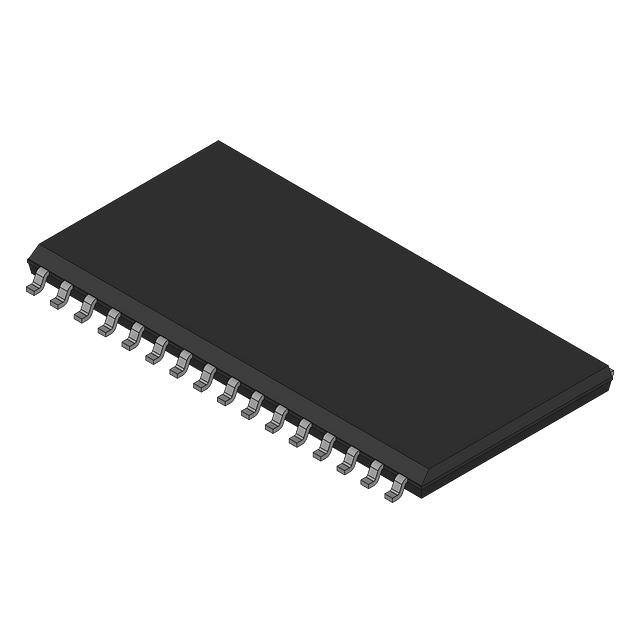
therefore, it is suitable for battery backup systems. It has packaged in 32-pin SOP, 32-pin TSOP II.
Features
• Single 5 V supply: 5 V ± 10%
• Access time: 55/70 ns (max)
• Power dissipation:
Active: 10 mW/MHz (typ)
Standby: 4 µW (typ)
• Completely static memory.
No clock or timing strobe required
• Equal access and cycle times
• Common data input and output.
Three state output
• Directly TTL compatible.
All inputs and outputs
• Battery backup operation.
• Operating temperature: −40 to +85°C
Rev.2.00, May.26.2004, page 1 of 12
�R1LP0408C-I Series
Ordering Information
Type No.
Access time
Package
R1LP0408CSP-5SI
55 ns
525-mil 32-pin plastic SOP (32P2M-A)
R1LP0408CSP-7LI
70 ns
R1LP0408CSB-5SI
55 ns
R1LP0408CSB-7LI
70 ns
R1LP0408CSC-5SI
55 ns
R1LP0408CSC-7LI
70 ns
Rev.2.00, May.26.2004, page 2 of 12
400-mil 32-pin plastic TSOP II (32P3Y-H)
400-mil 32-pin plastic TSOP II reverse (32P3Y-J)
�R1LP0408C-I Series
Pin Arrangement
32-pin SOP
32-pin TSOP
A18
A16
A14
A12
A7
A6
A5
A4
A3
A2
A1
A0
I/O0
I/O1
I/O2
VSS
1
2
3
4
5
6
7
8
9
10
11
12
13
14
15
16
32
31
30
29
28
27
26
25
24
23
22
21
20
19
18
17
(Top view)
Pin Description
Pin name
Function
A0 to A18
Address input
I/O0 to I/O7
Data input/output
CS# (CS)
Chip select
OE# (OE)
Output enable
WE# (WE)
Write enable
VCC
Power supply
VSS
Ground
Rev.2.00, May.26.2004, page 3 of 12
32-pin TSOP (reverse)
VCC
A15
A17
WE#
A13
A8
A9
A11
OE#
A10
CS#
I/O7
I/O6
I/O5
I/O4
I/O3
VCC
A15
A17
WE#
A13
A8
A9
A11
OE#
A10
CS#
I/O7
I/O6
I/O5
I/O4
I/O3
1
2
3
4
5
6
7
8
9
10
11
12
13
14
15
16
32
31
30
29
28
27
26
25
24
23
22
21
20
19
18
17
(Top view)
A18
A16
A14
A12
A7
A6
A5
A4
A3
A2
A1
A0
I/O0
I/O1
I/O2
VSS
�R1LP0408C-I Series
Block Diagram
LSB
MSB
V CC
A11
A9
A8
A15
A18
A10
A13
A17
A16
A14
A12
V SS
Row
Decoder
I/O0
•
•
•
•
•
Memory Matrix
2,048 × 2,048
•
•
Column I/O
Input
Data
Control
Column Decoder
I/O7
LSB A3 A2A1A0 A4 A5 A6 A7 MSB
••
CS#
WE#
Timing Pulse Generator
Read/Write Control
OE#
Rev.2.00, May.26.2004, page 4 of 12
•
•
�R1LP0408C-I Series
Operation Table
WE#
CS#
OE#
Mode
VCC current
I/O0 to I/O7
Ref. cycle
×
H
×
Not selected
ISB, ISB1
High-Z
H
L
H
Output disable
ICC
High-Z
H
L
L
Read
ICC
Dout
Read cycle
L
L
H
Write
ICC
Din
Write cycle (1)
L
L
L
Write
ICC
Din
Write cycle (2)
Note: H: VIH, L: VIL, ×: VIH or VIL
Absolute Maximum Ratings
Parameter
Symbol
Value
Power supply voltage relative to VSS
VCC
−0.5 to +7.0
Unit
V
1
2
Terminal voltage on any pin relative to VSS
VT
−0.5* to VCC + 0.3*
Power dissipation
PT
0.7
W
Operating temperature
Topr
−40 to +85
°C
Storage temperature range
Tstg
−65 to +150
°C
Storage temperature range under bias
Tbias
−40 to +85
°C
V
Notes: 1. VT min: −3.0 V for pulse half-width ≤ 30 ns.
2. Maximum voltage is +7.0 V.
DC Operating Conditions
(Ta = −40 to +85°C)
Parameter
Symbol
Min
Typ
Max
Unit
Supply voltage
VCC
4.5
5.0
5.5
V
VSS
0
0
0
V
VIH
2.2
VCC + 0.3
V
0.8
V
Input high voltage
Input low voltage
Note:
VIL
−0.3*
1. VIL min: −3.0 V for pulse half-width ≤ 30 ns.
Rev.2.00, May.26.2004, page 5 of 12
1
�R1LP0408C-I Series
DC Characteristics
Parameter
Symbol Min Typ
Input leakage current
|ILI|
1
µA
Vin = VSS to VCC
Output leakage current
|ILO|
1
µA
CS# = VIH or OE# = VIH or
WE# = VIL or VI/O = VSS to VCC
Operating current
ICC
1.5*1 3
mA
CS# = VIL,
Others = VIH/ VIL, II/O = 0 mA
Average operating current
ICC1
8*1
25
mA
Min. cycle, duty = 100%,
CS# = VIL, Others = VIH/VIL
II/O = 0 mA
ICC2
2*1
5
mA
Cycle time = 1 µs,
duty = 100%,
II/O = 0 mA, CS# ≤ 0.2 V,
VIH ≥ VCC − 0.2 V, VIL ≤ 0.2 V
ISB
0.1*1 0.5
mA
CS# = VIH
to +85°C
ISB1
10
µA
Vin ≥ 0 V, CS# ≥ VCC − 0.2 V
to +70°C
ISB1
Standby current
Standby current
−5SI
to +40°C
−7LI
ISB1
Max Unit Test conditions
8
µA
2
3
µA
1
1.0*
to +25°C
ISB1
0.8*
3
µA
to +85°C
ISB1
20
µA
to +70°C
ISB1
to +40°C
ISB1
16
µA
2
10
µA
1
1.0*
ISB1
0.8*
10
µA
Output low voltage
VOL
0.4
V
IOL = 2.1 mA
Output high voltage
VOH
2.4
V
IOH = −1.0 mA
VOH2
2.6
V
IOH = −0.1 mA
to +25°C
Notes: 1. Typical values are at VCC = 5.0 V, Ta = +25°C and specified loading, and not guaranteed.
2. Typical values are at VCC = 5.0 V, Ta = +40°C and specified loading, and not guaranteed.
Capacitance
(Ta = +25°C, f = 1.0 MHz)
Parameter
Symbol
Min
Typ
Max
Unit
Test conditions
Note
Input capacitance
Cin
8
pF
Vin = 0 V
1
Input/output capacitance
CI/O
10
pF
VI/O = 0 V
1
Note:
1. This parameter is sampled and not 100% tested.
Rev.2.00, May.26.2004, page 6 of 12
�R1LP0408C-I Series
AC Characteristics
(Ta = −40 to +85°C, VCC = 5 V ± 10%, unless otherwise noted.)
Test Conditions
•
•
•
•
Input pulse levels: VIL = 0.4 V, VIH = 2.4 V
Input rise and fall time: 5 ns
Input and output timing reference levels: 1.5 V
Output load: 1 TTL Gate + CL (50 pF) (R1LP0408C-5SI)
1 TTL Gate + CL (100 pF) (R1LP0408C-7LI)
(Including scope and jig)
Read Cycle
R1LP0408C-I
-5SI
-7LI
Parameter
Symbol
Min
Max
Min
Max
Unit
Read cycle time
tRC
55
70
ns
Address access time
tAA
55
70
ns
Chip select access time
tCO
55
70
ns
Output enable to output valid
tOE
25
35
ns
Chip select to output in low-Z
tLZ
10
10
ns
2
Output enable to output in low-Z
tOLZ
5
5
ns
2
Chip deselect to output in high-Z
tHZ
0
20
0
25
ns
1, 2
Output disable to output in high-Z
tOHZ
0
20
0
25
ns
1, 2
Output hold from address change
tOH
10
10
ns
Rev.2.00, May.26.2004, page 7 of 12
Notes
�R1LP0408C-I Series
Write Cycle
R1LP0408C-I
-5SI
-7LI
Parameter
Symbol
Min
Max
Min
Max
Unit
Notes
Write cycle time
tWC
55
70
ns
Chip selection to end of write
tCW
50
60
ns
4
Address setup time
tAS
0
0
ns
5
Address valid to end of write
tAW
50
60
ns
Write pulse width
tWP
40
50
ns
3, 12
Write recovery time
tWR
0
0
ns
6
Write to output in high-Z
tWHZ
0
20
0
25
ns
1, 2, 7
Data to write time overlap
tDW
25
30
ns
Data hold from write time
tDH
0
0
ns
Output active from end of write
tOW
5
5
ns
2
Output disable to output in high-Z
tOHZ
0
20
0
25
ns
1, 2, 7
Notes: 1. tHZ, tOHZ and tWHZ are defined as the time at which the outputs achieve the open circuit conditions
and are not referred to output voltage levels.
2. This parameter is sampled and not 100% tested.
3. A write occurs during the overlap (tWP) of a low CS# and a low WE#. A write begins at the later
transition of CS# going low or WE# going low. A write ends at the earlier transition of CS# going
high or WE# going high. tWP is measured from the beginning of write to the end of write.
4. tCW is measured from CS# going low to the end of write.
5. tAS is measured from the address valid to the beginning of write.
6. tWR is measured from the earlier of WE# or CS# going high to the end of write cycle.
7. During this period, I/O pins are in the output state so that the input signals of the opposite phase
to the outputs must not be applied.
8. If the CS# low transition occurs simultaneously with the WE# low transition or after the WE#
transition, the output remain in a high impedance state.
9. Dout is the same phase of the write data of this write cycle.
10. Dout is the read data of next address.
11. If CS# is low during this period, I/O pins are in the output state. Therefore, the input signals of
the opposite phase to the outputs must not be applied to them.
12. In the write cycle with OE# low fixed, tWP must satisfy the following equation to avoid a problem of
data bus contention. tWP ≥ tDW min + tWHZ max
Rev.2.00, May.26.2004, page 8 of 12
�R1LP0408C-I Series
Timing Waveform
Read Timing Waveform (WE# = VIH)
tRC
Address
Valid address
tAA
tCO
CS#
tLZ
tHZ
tOE
tOLZ
OE#
tOHZ
Dout
High impedance
Valid data
tOH
Rev.2.00, May.26.2004, page 9 of 12
�R1LP0408C-I Series
Write Timing Waveform (1) (OE# Clock)
tWC
Address
Valid address
tAW
tWR
OE#
tCW
CS#
*8
tWP
tAS
WE#
tOHZ
Dout
High impedance
tDW
Din
Rev.2.00, May.26.2004, page 10 of 12
Valid data
tDH
�R1LP0408C-I Series
Write Timing Waveform (2) (OE# Low Fixed)
tWC
Address
Valid address
tCW
tWR
CS#
*8
tAW
tWP
WE#
tOH
tAS
tOW
tWHZ
*9
Dout
High impedance
tDW
tDH
*11
Din
Rev.2.00, May.26.2004, page 11 of 12
Valid data
*10
�R1LP0408C-I Series
Low VCC Data Retention Characteristics
(Ta = −40 to +85°C)
Symbol Min Typ
VCC for data retention
VDR
2
V
CS# ≥ VCC − 0.2 V, Vin ≥ 0 V
to +85°C
ICCDR
10
µA
VCC = 3.0 V, Vin ≥ 0 V
to +70°C
ICCDR
8
µA
CS# ≥ VCC − 0.2 V
to +40°C
ICCDR
1.0*2 3
µA
to +25°C
ICCDR
0.8*1 3
µA
to +85°C
ICCDR
20
µA
to +70°C
ICCDR
Data
retention
current
−5SI
−7LI
to +40°C
ICCDR
Max Unit Test conditions*
3
Parameter
16
µA
1.0*
2
10
µA
1
10
µA
ICCDR
0.8*
Chip deselect to data retention time
tCDR
0
ns
Operation recovery time
tR
tRC*4
ns
to +25°C
See retention waveform
Notes: 1. Typical values are at VCC = 3.0 V, Ta = +25°C and specified loading, and not guaranteed.
2. Typical values are at VCC = 3.0 V, Ta = +40°C and specified loading, and not guaranteed.
3. CS# controls address buffer, WE# buffer, OE# buffer, and Din buffer. In data retention mode,
Vin levels (address, WE#, OE#, I/O) can be in the high impedance state.
4. tRC = read cycle time.
Low VCC Data Retention Timing Waveform (CS# Controlled)
tCDR
Data retention mode
VCC
4.5 V
2.2 V
VDR
CS#
0V
Rev.2.00, May.26.2004, page 12 of 12
CS# ≥ VCC – 0.2 V
tR
�Revision History
Rev.
Date
R1LP0408C-I Series Data Sheet
Contents of Modification
Page
Description
1.00
Aug.01.2003
Initial issue
2.00
May.26.2004
6
DC characteristics
−5SI and −7LI items’ description are divided.
12
Low VCC Data Retention Characteristics
−5SI and −7LI items’ description are divided.
12
Low VCC Data Retention Timing Waveform
2.4 V to 2.2 V
�Sales Strategic Planning Div.
Nippon Bldg., 2-6-2, Ohte-machi, Chiyoda-ku, Tokyo 100-0004, Japan
Keep safety first in your circuit designs!
1. Renesas Technology Corp. puts the maximum effort into making semiconductor products better and more reliable, but there is always the possibility that trouble
may occur with them. Trouble with semiconductors may lead to personal injury, fire or property damage.
Remember to give due consideration to safety when making your circuit designs, with appropriate measures such as (i) placement of substitutive, auxiliary
circuits, (ii) use of nonflammable material or (iii) prevention against any malfunction or mishap.
Notes regarding these materials
1. These materials are intended as a reference to assist our customers in the selection of the Renesas Technology Corp. product best suited to the customer's
application; they do not convey any license under any intellectual property rights, or any other rights, belonging to Renesas Technology Corp. or a third party.
2. Renesas Technology Corp. assumes no responsibility for any damage, or infringement of any third-party's rights, originating in the use of any product data,
diagrams, charts, programs, algorithms, or circuit application examples contained in these materials.
3. All information contained in these materials, including product data, diagrams, charts, programs and algorithms represents information on products at the time of
publication of these materials, and are subject to change by Renesas Technology Corp. without notice due to product improvements or other reasons. It is
therefore recommended that customers contact Renesas Technology Corp. or an authorized Renesas Technology Corp. product distributor for the latest product
information before purchasing a product listed herein.
The information described here may contain technical inaccuracies or typographical errors.
Renesas Technology Corp. assumes no responsibility for any damage, liability, or other loss rising from these inaccuracies or errors.
Please also pay attention to information published by Renesas Technology Corp. by various means, including the Renesas Technology Corp. Semiconductor
home page (http://www.renesas.com).
4. When using any or all of the information contained in these materials, including product data, diagrams, charts, programs, and algorithms, please be sure to
evaluate all information as a total system before making a final decision on the applicability of the information and products. Renesas Technology Corp. assumes
no responsibility for any damage, liability or other loss resulting from the information contained herein.
5. Renesas Technology Corp. semiconductors are not designed or manufactured for use in a device or system that is used under circumstances in which human life
is potentially at stake. Please contact Renesas Technology Corp. or an authorized Renesas Technology Corp. product distributor when considering the use of a
product contained herein for any specific purposes, such as apparatus or systems for transportation, vehicular, medical, aerospace, nuclear, or undersea repeater
use.
6. The prior written approval of Renesas Technology Corp. is necessary to reprint or reproduce in whole or in part these materials.
7. If these products or technologies are subject to the Japanese export control restrictions, they must be exported under a license from the Japanese government and
cannot be imported into a country other than the approved destination.
Any diversion or reexport contrary to the export control laws and regulations of Japan and/or the country of destination is prohibited.
8. Please contact Renesas Technology Corp. for further details on these materials or the products contained therein.
http://www.renesas.com
RENESAS SALES OFFICES
Renesas Technology America, Inc.
450 Holger Way, San Jose, CA 95134-1368, U.S.A
Tel: (408) 382-7500 Fax: (408) 382-7501
Renesas Technology Europe Limited.
Dukes Meadow, Millboard Road, Bourne End, Buckinghamshire, SL8 5FH, United Kingdom
Tel: (1628) 585 100, Fax: (1628) 585 900
Renesas Technology Europe GmbH
Dornacher Str. 3, D-85622 Feldkirchen, Germany
Tel: (89) 380 70 0, Fax: (89) 929 30 11
Renesas Technology Hong Kong Ltd.
7/F., North Tower, World Finance Centre, Harbour City, Canton Road, Hong Kong
Tel: 2265-6688, Fax: 2375-6836
Renesas Technology Taiwan Co., Ltd.
FL 10, #99, Fu-Hsing N. Rd., Taipei, Taiwan
Tel: (2) 2715-2888, Fax: (2) 2713-2999
Renesas Technology (Shanghai) Co., Ltd.
26/F., Ruijin Building, No.205 Maoming Road (S), Shanghai 200020, China
Tel: (21) 6472-1001, Fax: (21) 6415-2952
Renesas Technology Singapore Pte. Ltd.
1, Harbour Front Avenue, #06-10, Keppel Bay Tower, Singapore 098632
Tel: 6213-0200, Fax: 6278-8001
© 2004. Renesas Technology Corp., All rights reserved. Printed in Japan.
Colophon .1.0
�Selection Guide
Low Power SRAM
www.renesas.eu
2010.11
�About Renesas Electronics Corporation
Renesas Electronics Corporation (TSE: 6723), the world’s number one supplier of microcontrollers, is a premier supplier of
advanced semiconductor solutions including microcontrollers, SoC solutions and a broad range of analog and power devices
as well as memory products. Business operations began as Renesas Electronics in April 2010 through the integration of
NEC Electronics Corporation (TSE:6723) and Renesas Technology Corp., with operations spanning research, development,
design and manufacturing for a wide range of applications. Headquartered in Japan, Renesas Electronics has subsidiaries in
20 countries worldwide. More information can be found at www.renesas.com.
Welcome to the Low Power SRAM product lineup
Renesas memory delivers superior reliability achieved through exclusive advanced technology. An extensive line-up of memory
products is available to meet the diverse functional requirements of our customers, covering not only Low Power SRAM, but
also QDRII, QDRII+, DDRII & DDRII+ High Speed SRAM and a wide range of serial/parallel EEPROM.
Roadmap
Low Power SRAM
2010
2013
2014
2015
Status
in MP
MP Advanced Version from Q2'11
3 V x8 0.25 µm
0.15 µm Advanced
in MP
MP Advanced Version from Q1'11
5 V x8 0.25 µm
0.15 µm Advanced
in MP
3 V x8/x16 0.25 µm
0.15 µm Advanced
in MP
MP Advanced Version from Q2'11
3 V x8/x16
0.15 µm Advanced
in MP
5 V x8
0.18 µm
in MP
3 V x8/x16
0.15 µm Advanced
in MP
5 V x8/x16
0.18 µm
in MP
16 Mbit 3 V x8/x16
0.13 µm CMOS
in MP
16 Mbit 3 V x8/x16
0.15 µm Advanced
in MP
32 Mbit 3 V x8/x16
0.15 µm Advanced
in MP
64 Mbit 3 V x8/x16
0.15 µm Advanced
in MP
1 Mbit
2 Mbit
4 Mbit
Middle
8 Mbit
High
2012
0.15 µm Advanced
256 kbit 3 V/5 V x8 0.6 µm
Low
2011
• Widest product line-up from 256 kbit – 64 Mbit
• Long term and stable support
• Highest quality due to Renesas core advanced technology
• Easy switch to higher density in the same package
• In house R & D and Fabs
2
www.renesas.eu
�Renesas offers the best quality – our biggest strength
Our advanced technology achieves outstanding results:
• High reliability
• Smaller die size
• Latch-up free
• Soft-error free
SRAM = 6 Transistors
Transistor 1
Transistor 2
Transistor 3
Transistor 4
Transistor 5
Transistor 6
90 nm process:
Process itself is smaller but Transistors are bigger, as they need to store a big amount of charge.
Transistor 1
Renesas 150 nm process:
Capacitor
Transistor 2
Capacitor
Transistor 3
Transistor 4
Cell of Renesas core advanced technology, about half the size of full CMOS.
How did we achieve such high quality?
Renesas uses TFT MOSFETs instead of planar MOSFETs. Additionally in the devices, a large amount of charge is stored in two
capacitors which subsequently increases the capacitance of the TFTs. These capacitors are positioned above the TFTs, in turn
shielding the transistors from alpha and neutron radiation. Together this makes Renesas’ SRAM cells latch-up free and enables
the lowest soft-error rate in the industry.
We are proud to confirm...
Soft Error Rate of our advanced technology has been tested and confirmed to be less than 100FIT/device.
3
�Package Lineup for Renesas Low Power SRAM
1.27
256 Kb
FBGA
uTSOP(II)
0.5
0.5
8
1 Mb
20
1.27
1/2/4
Mb
11.76
14.1
1/4 Mb
8
13.4
17.5
4 Mb
13.4
x8
config.
1.27
20.75
20.95
2/4/8 Mb
44-pin
x8 / x16
config.
11.76
32-pin
TSOP(II)
sTSOP(I)
8
256 Kb
0.55
28-pin
TSOP(I)
11.93
SOP
0.8
7.5-8.0
20.00
8/16/32
64 Mb
52-pin
4/8/16/32
64 Mb*
10.49
0.5
(48-ball)
12.00
8/16/32
64 Mb
48-pin
8.5-9.5
18.41
0.4
10.79
* Package size for 64 Mb FBGA is 8.5 mm x 11 mm.
Renesas provides six kinds of packages, which are upwards compatible, making it easy to expand density without changing the PCB.
Low Power SRAM Part Numbering System
R1 L V 16 16 R SD - 7 S I
Renesas Memory
Chip configuration of LPSRAM
L Single chip
W Two chip (MCP)
Operating Voltage
V 3V
P 5V
Density
01 1 Mb
02 2 Mb
04 4 Mb
08 8 Mb
16 16 Mb
32 32 Mb
64 64 Mb
Bit configuration
08 x8
16 x16 or x8/x16 (Byte# control)
Chip Generation
4
Operating Temperature
R
0 ~ 70°C
C -20 ~ 70°C
I -40 ~ 85°C
Stand by current /
Data retention current
L Standard
S Low power version
Access Time
7 70 ns
5 55 ns
4 45 ns
Package
SA sTSOP (1Mb/2Mb/4Mb)
TSOPI (8Mb/16Mb/32Mb/64Mb)
SB TSOPII
SC rev.TSOPII (4Mb)
SD µTSOPII
SF TSOPI (1Mb)
SP SOP
SR rev.TSOPI (1Mb)
BG FBGA
www.renesas.eu
�Useful Links
Datasheet
http://www.renesas.eu/products/memory/low_power_sram/lpsram_root.jsp
Advanced 0.15 µm Technology
http://www.renesas.eu/products/memory/low_power_sram/child_folder/lpsram_supersram.jsp
Technical update
http://www.renesas.eu/products/memory/low_power_sram/Technical_Update.jsp
Franchised distributors
http://www.renesas.eu/support/purchasing_info/purchasing_info.jsp?title=European%2520Distributors
5
�Product List
Capacity Configuration
Suffix
Package
Voltage
Temperature
Comments
32 k x 8
R1LP5256ESP-5SR
R1LP5256ESP-7SR
R1LP5256ESA-5SR
R1LP5256ESA-7SR
#B0 #S0
SOP(28)
SOP(28)
TSOP(28)
TSOP(28)
55
70
0.15 µm
4.5 V to 5.5 V
0 to 70 °C
Mass production from Q2’11
32 k x 8
R1LP5256ESP-5SI
R1LP5256ESP-7SI
R1LP5256ESA-5SI
R1LP5256ESA-7SI
#B0 #S0
SOP(28)
SOP(28)
TSOP(28)
TSOP(28)
55
70
0.15 µm
4.5 V to 5.5 V
-40 to 85 °C
Mass production from Q2’11
32 k x 8
R1LV5256ESP-5SR
R1LV5256ESP-7SR
R1LV5256ESA-5SR
R1LV5256ESA-7SR
#B0 #S0
SOP(28)
SOP(28)
TSOP(28)
TSOP(28)
55
70
0.15 µm
2.7 V to 3.6 V
0 to 70 °C
Mass production from Q2’11
32 k x 8
R1LV5256ESP-5SI
R1LV5256ESP-7SI
R1LV5256ESA-5SI
R1LV5256ESA-7SI
#B0 #S0
SOP(28)
SOP(28)
TSOP(28)
TSOP(28)
55
70
0.15 µm
2.7 V to 3.6 V
-40 to 85 °C
Mass production from Q2’11
128 k x 8
R1LP0108ESP-5SR
R1LP0108ESP-7SR
R1LP0108ESF-5SR
R1LP0108ESF-7SR
R1LP0108ESR-5SR
R1LP0108ESR-7SR
R1LP0108ESA-5SR
R1LP0108ESA-7SR
#B0 #S0
SOP(32)
SOP(32)
TSOP(32)
TSOP(32)
rev.TSOP(32)
rev.TSOP(32)
sTSOP(32)
sTSOP(32)
55
70
0.15 µm
4.5 V to 5.5 V
0 to 70 °C
128 k x 8
R1LP0108ESP-5SI
R1LP0108ESP-7SI
R1LP0108ESF-5SI
R1LP0108ESF-7SI
R1LP0108ESR-5SI
R1LP0108ESR-7SI
R1LP0108ESA-5SI
R1LP0108ESA-7SI
#B0 #S0
SOP(32)
SOP(32)
TSOP(32)
TSOP(32)
rev.TSOP(32)
rev.TSOP(32)
sTSOP(32)
sTSOP(32)
55
70
0.15 µm
4.5 V to 5.5 V
-40 to 85 °C
128 k x 8
R1LV0108ESP-5SR
R1LV0108ESP-7SR
R1LV0108ESF-5SR
R1LV0108ESF-7SR
R1LV0108ESA-5SR
R1LV0108ESA-7SR
#B0 #S0
SOP(32)
SOP(32)
TSOP(32)
TSOP(32)
sTSOP(32)
sTSOP(32)
55
70
0.15 µm
2.7 V to 3.6 V
0 to 70 °C
Mass production from Q1’11
128 k x 8
R1LV0108ESP-5SI
R1LV0108ESP-7SI
R1LV0108ESF-5SI
R1LV0108ESF-7SI
R1LV0108ESA-5SI
R1LV0108ESA-7SI
#B0 #S0
SOP(32)
SOP(32)
TSOP(32)
TSOP(32)
sTSOP(32)
sTSOP(32)
55
70
0.15 µm
2.7 V to 3.6 V
-40 to 85 °C
Mass production from Q1’11
256 k x 8
R1LV0208BSA-5SI
R1LV0208BSA-7SI
#B0 #S0
sTSOP(32)
55
70
0.15 µm
2.7 V to 3.6 V
-40 to 85 °C
Mass production from Q2’11
128 k x 16
R1LV0216BSB-5SI
R1LV0216BSB-7SI
#B0 #S0
TSOP(44)
55
70
0.15 µm
2.7 V to 3.6 V
-40 to 85 °C
Mass production from Q2’11
R1LP0408CSP-5SC
R1LP0408CSP-7LC
R1LP0408CSB-5SC
R1LP0408CSB-7LC
R1LP0408CSC-5SC
R1LP0408CSC-7LC
#B0 #S0
SOP(32)
SOP(32)
TSOP(32)
TSOP(32)
rev.TSOP(32)
rev.TSOP(32)
55
70
0.18 µm
4.5 V to 5.5 V
-20 to 70 °C
R1LP0408CSP-5SI
R1LP0408CSP-7LI
R1LP0408CSB-5SI
R1LP0408CSB-7LI
R1LP0408CSC-5SI
R1LP0408CSC-7LI
#B0 #S0
SOP(32)
SOP(32)
TSOP(32)
TSOP(32)
rev.TSOP(32)
rev.TSOP(32)
55
70
0.18 µm
4.5 V to 5.5 V
-40 to 85 °C
R1LV0408DSP-5SR
R1LV0408DSP-7LR
R1LV0408DSA-5SR
R1LV0408DSA-7LR
R1LV0408DSB-5SR
R1LV0408DSB-7LR
#B0 #S0
SOP(32)
SOP(32)
sTSOP(32)
sTSOP(32)
TSOP(32)
TSOP(32)
55
70
0.15 µm
2.7 V to 3.6 V
0 to 70 °C
R1LV0408DSP-5SI
R1LV0408DSP-7LI
R1LV0408DSA-5SI
R1LV0408DSA-7LI
R1LV0408DSB-5SI
R1LV0408DSB-7LI
#B0 #S0
SOP(32)
SOP(32)
sTSOP(32)
sTSOP(32)
TSOP(32)
TSOP(32)
55
70
0.15 µm
2.7 V to 3.6 V
-40 to 85 °C
256 kbit
1 Mbit
2 Mbit
512 k x 8
512 k x 8
4 Mbit
512 k x 8
512 k x 8
6
Access
Process
Time (ns)
Part Name
#D0 #S0
#D0 #S0
#D0 #S0
#D0 #S0
#B0 #S0
#B0 #S0
#B0 #S0
#B0 #S0
www.renesas.eu
�Capacity Configuration
4 Mbit
8 Mbit
Suffix
Package
256 k x 16
R1LV0416DSB-5SR
R1LV0416DSB-7LR
#B0 #S0
TSOP(44)
55
70
256 k x 16
R1LV0416DSB-5SI
R1LV0416DSB-7LI
#B0 #S0
TSOP(44)
256 k x 16
R1LV0416DBG-5SR
R1LV0416DBG-7LR
#B0 #S0
256 k x 16
R1LV0416DBG-5SI
R1LV0416DBG-7LI
256 k x 16
256 k x 16
32 Mbit
64 Mbit
(MCP)
Voltage
Temperature
Comments
0.15 µm
2.7 V to 3.6 V
0 to 70 °C
2-chip select
55
70
0.15 µm
2.7 V to 3.6 V
-40 to 85 °C
2-chip select
FBGA(48)
55
70
0.15 µm
2.7 V to 3.6 V
0 to 70 °C
2-chip select
#B0 #S0
FBGA(48)
55
70
0.15 µm
2.7 V to 3.6 V
-40 to 85 °C
2-chip select
R1LV0414DSB-5SR
R1LV0414DSB-7LR
#B0 #S0
TSOP(44)
55
70
0.15 µm
2.7 V to 3.6 V
0 to 70 °C
1-chip select
R1LV0414DSB-5SI
R1LV0414DSB-7LI
#B0 #S0
TSOP(44)
55
70
0.15 µm
2.7 V to 3.6 V
-40 to 85 °C
1-chip select
former HM628100LTTI-5SL
1M x 8
HM28100TTI5SE
TSOP(44)
55
0.18 µm
5.0 V ± 10%
-40 to 85 °C
1M x 8
R1LV0808ASB-5SI
R1LV0808ASB-7SI
#B0 #S0
TSOP(44)
55
70
0.15 µm
2.4 V to 3.6 V
-40 to 85 °C
1 M x 8/
512 k x 16
R1LV0816ASD-5SI
R1LV0816ASD-7SI
#B0 #S0
µTSOP(52)
55
70
0.15 µm
2.4 V to 3.6 V
-40 to 85 °C
512 k x 16
HM216514TTI5SE
TSOP(44)
55
0.18 µm
4.5 V to 5.5 V
-40 to 85 °C
1 M x 8/
512 k x 16
R1LV0816ASA-5SI
R1LV0816ASA-7SI
#B0 #S0
TSOP(48)
NEW
55
70
0.15 µm
2.4 V to 3.6 V
-40 to 85 °C
512 k x 16
R1LV0816ASB-5SI
R1LV0816ASB-7SI
#B0 #S0
TSOP(44)
55
70
0.15 µm
2.4 V to 3.6 V
-40 to 85 °C
512 k x 16
R1LV0816ABG-5SI
R1LV0816ABG-7SI
#B0 #S0
FBGA(48)
FBGA(48)
55
70
0.15 µm
2.4 V to 3.6 V
-40 to 85 °C
2 M x 8/
1 M x 16
R1LV1616RSD-7SR
R1LV1616RSD-7SI
#B0 #S0
µTSOP(52)
70
85
0.15 µm
2.7 V to 3.6 V
0 to 70 °C
-40 to 85 °C
2 M x 8/
1 M x 16
R1LV1616RSD-5SR
R1LV1616RSD-5SI
#B0 #S0
µTSOP(52)
55
0.15 µm
2.7 V to 3.6 V
0 to 70 °C
-40 to 85 °C
2 M x 8/
1 M x 16
R1LV1616RSA-5SR
R1LV1616RSA-7SR
R1LV1616RSA-5SI
R1LV1616RSA-7SI
#B0 #S0
TSOP(48)
55
70
85
0.15 µm
2.7 V to 3.6 V
0 to 70 °C
0 to 70 °C
-40 to 85 °C
-40 to 85 °C
2 M x 8/
1 M x 16
R1LV1616HSA-4SI
R1LV1616HSA-5SI
#B0 #S0
TSOP(48)
45
55
0.13 µm
2.7 V to 3.6 V
-40 to 85 °C
1 M x 16
R1LV1616RBG-7SR
R1LV1616RBG-7SI
#B0 #S0
FBGA(48)
70
85
0.15 µm
2.7 V to 3.6 V
0 to 70 °C
-40 to 85 °C
1 M x 16
R1LV1616RBG-5SR
R1LV1616RBG-5SI
#B0 #S0
FBGA(48)
55
0.15 µm
2.7 V to 3.6 V
0 to 70 °C
-40 to 85 °C
1 M x 16
R1LV1616HBG-4SI
R1LV1616HBG-5SI
#B0 #S0
FBGA(48)
45
55
0.13 µm
2.7 V to 3.6 V
-40 to 85 °C
2 M x 16
R1WV3216RBG-7SR
R1WV3216RBG-7SI
#B0 #S0
FBGA(48)
70
85
0.15 µm
2.7 V to 3.6 V
0 to 70 °C
-40 to 85 °C
4 M x 8/
2 M x 16
R1LV3216RSA-5SR
R1LV3216RSA-7SR
R1LV3216RSA-5SI
R1LV3216RSA-7SI
#B0 #S0
TSOP(48)
55
70
0.15 µm
2.7 V to 3.6 V
0 to 70 °C
0 to 70 °C
-40 to 85 °C
-40 to 85 °C
4 M x 8/
2 M x 16
R1LV3216RSD-5SR
R1LV3216RSD-7SR
R1LV3216RSD-5SI
R1LV3216RSD-7SI
#B0 #S0
µTSOP(52)
55
70
0.15 µm
2.7 V to 3.6 V
0 to 70 °C
0 to 70 °C
-40 to 85 °C
-40 to 85 °C
4 M x 16
R1WV6416RBG-5SR
R1WV6416RBG-7SR
R1WV6416RBG-5SI
R1WV6416RBG-7SI
#B0 #S0
FBGA(48)
55
70
0.15 µm
2.7 V to 3.6 V
0 to 70 °C
0 to 70 °C
-40 to 85 °C
-40 to 85 °C
8 M x 8/
4 M x 16
R1WV6416RSA-5SR
R1WV6416RSA-7SR
R1WV6416RSA-5SI
R1WV6416RSA-7SI
#B0 #S0
TSOP(48)
55
70
0.15 µm
2.7 V to 3.6 V
0 to 70 °C
0 to 70 °C
-40 to 85 °C
-40 to 85 °C
8 M x 8/
4 M x 16
R1WV6416RSD-5SR
R1WV6416RSD-7SR
R1WV6416RSD-5SI
R1WV6416RSD-7SI
#B0 #S0
µTSOP(52)
55
70
0.15 µm
2.7 V to 3.6 V
0 to 70 °C
0 to 70 °C
-40 to 85 °C
-40 to 85 °C
16 Mbit
32 Mbit
(MCP)
Access
Process
Time (ns)
Part Name
former HM6216514LTTI-5SL
All our parts are RoHS compliant. Suffix: #B0 is indicating loose parts. Suffix #S0 is indicating Tape + Reel (1,000 pcs. per reel). MCP: Multi Chip Package
7
�Low Power SRAM
Before purchasing or using any Renesas Electronics products listed herein, please refer to the latest product manual and/or data sheet in advance.
www.renesas.eu
© 2010 Renesas Electronics Europe.
All rights reserved. Printed in Germany.
Document No. R10PF0003ED0100
�


 工商网监
湘ICP备2023018690号
工商网监
湘ICP备2023018690号
