To our customers,
Old Company Name in Catalogs and Other Documents
On April 1st, 2010, NEC Electronics Corporation merged with Renesas Technology
Corporation, and Renesas Electronics Corporation took over all the business of both
companies. Therefore, although the old company name remains in this document, it is a valid
Renesas Electronics document. We appreciate your understanding.
Renesas Electronics website: http://www.renesas.com
April 1st, 2010
Renesas Electronics Corporation
Issued by: Renesas Electronics Corporation (http://www.renesas.com)
Send any inquiries to http://www.renesas.com/inquiry.
�Notice
1.
2.
3.
4.
5.
6.
7.
All information included in this document is current as of the date this document is issued. Such information, however, is
subject to change without any prior notice. Before purchasing or using any Renesas Electronics products listed herein, please
confirm the latest product information with a Renesas Electronics sales office. Also, please pay regular and careful attention to
additional and different information to be disclosed by Renesas Electronics such as that disclosed through our website.
Renesas Electronics does not assume any liability for infringement of patents, copyrights, or other intellectual property rights
of third parties by or arising from the use of Renesas Electronics products or technical information described in this document.
No license, express, implied or otherwise, is granted hereby under any patents, copyrights or other intellectual property rights
of Renesas Electronics or others.
You should not alter, modify, copy, or otherwise misappropriate any Renesas Electronics product, whether in whole or in part.
Descriptions of circuits, software and other related information in this document are provided only to illustrate the operation of
semiconductor products and application examples. You are fully responsible for the incorporation of these circuits, software,
and information in the design of your equipment. Renesas Electronics assumes no responsibility for any losses incurred by
you or third parties arising from the use of these circuits, software, or information.
When exporting the products or technology described in this document, you should comply with the applicable export control
laws and regulations and follow the procedures required by such laws and regulations. You should not use Renesas
Electronics products or the technology described in this document for any purpose relating to military applications or use by
the military, including but not limited to the development of weapons of mass destruction. Renesas Electronics products and
technology may not be used for or incorporated into any products or systems whose manufacture, use, or sale is prohibited
under any applicable domestic or foreign laws or regulations.
Renesas Electronics has used reasonable care in preparing the information included in this document, but Renesas Electronics
does not warrant that such information is error free. Renesas Electronics assumes no liability whatsoever for any damages
incurred by you resulting from errors in or omissions from the information included herein.
Renesas Electronics products are classified according to the following three quality grades: “Standard”, “High Quality”, and
“Specific”. The recommended applications for each Renesas Electronics product depends on the product’s quality grade, as
indicated below. You must check the quality grade of each Renesas Electronics product before using it in a particular
application. You may not use any Renesas Electronics product for any application categorized as “Specific” without the prior
written consent of Renesas Electronics. Further, you may not use any Renesas Electronics product for any application for
which it is not intended without the prior written consent of Renesas Electronics. Renesas Electronics shall not be in any way
liable for any damages or losses incurred by you or third parties arising from the use of any Renesas Electronics product for an
application categorized as “Specific” or for which the product is not intended where you have failed to obtain the prior written
consent of Renesas Electronics. The quality grade of each Renesas Electronics product is “Standard” unless otherwise
expressly specified in a Renesas Electronics data sheets or data books, etc.
“Standard”:
8.
9.
10.
11.
12.
Computers; office equipment; communications equipment; test and measurement equipment; audio and visual
equipment; home electronic appliances; machine tools; personal electronic equipment; and industrial robots.
“High Quality”: Transportation equipment (automobiles, trains, ships, etc.); traffic control systems; anti-disaster systems; anticrime systems; safety equipment; and medical equipment not specifically designed for life support.
“Specific”:
Aircraft; aerospace equipment; submersible repeaters; nuclear reactor control systems; medical equipment or
systems for life support (e.g. artificial life support devices or systems), surgical implantations, or healthcare
intervention (e.g. excision, etc.), and any other applications or purposes that pose a direct threat to human life.
You should use the Renesas Electronics products described in this document within the range specified by Renesas Electronics,
especially with respect to the maximum rating, operating supply voltage range, movement power voltage range, heat radiation
characteristics, installation and other product characteristics. Renesas Electronics shall have no liability for malfunctions or
damages arising out of the use of Renesas Electronics products beyond such specified ranges.
Although Renesas Electronics endeavors to improve the quality and reliability of its products, semiconductor products have
specific characteristics such as the occurrence of failure at a certain rate and malfunctions under certain use conditions. Further,
Renesas Electronics products are not subject to radiation resistance design. Please be sure to implement safety measures to
guard them against the possibility of physical injury, and injury or damage caused by fire in the event of the failure of a
Renesas Electronics product, such as safety design for hardware and software including but not limited to redundancy, fire
control and malfunction prevention, appropriate treatment for aging degradation or any other appropriate measures. Because
the evaluation of microcomputer software alone is very difficult, please evaluate the safety of the final products or system
manufactured by you.
Please contact a Renesas Electronics sales office for details as to environmental matters such as the environmental
compatibility of each Renesas Electronics product. Please use Renesas Electronics products in compliance with all applicable
laws and regulations that regulate the inclusion or use of controlled substances, including without limitation, the EU RoHS
Directive. Renesas Electronics assumes no liability for damages or losses occurring as a result of your noncompliance with
applicable laws and regulations.
This document may not be reproduced or duplicated, in any form, in whole or in part, without prior written consent of Renesas
Electronics.
Please contact a Renesas Electronics sales office if you have any questions regarding the information contained in this
document or Renesas Electronics products, or if you have any other inquiries.
(Note 1) “Renesas Electronics” as used in this document means Renesas Electronics Corporation and also includes its majorityowned subsidiaries.
(Note 2) “Renesas Electronics product(s)” means any product developed or manufactured by or for Renesas Electronics.
�R1LV0414D Series
4M SRAM (256-kword × 16-bit)
REJ03C0312-0100
Rev.1.00
May.24.2007
Description
The R1LV0414D is a 4-Mbit static RAM organized 256-kword × 16-bit, fabricated by Renesas’s high-performance
0.15µm CMOS and TFT technologies. R1LV0414DSeries has realized higher density, higher performance and low
power consumption. The R1LV0414D Series offers low power standby power dissipation; therefore, it is suitable for
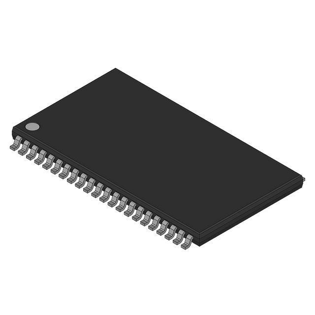
battery backup systems. It has packaged in 44-pin TSOP II.
Features
• Single 3.0 V supply: 2.7 V to 3.6 V
• Fast access time: 55/70 ns (max)
• Power dissipation:
Standby: 3 µW (typ) (VCC = 3.0 V)
• Equal access and cycle times
• Common data input and output.
Three state output
• Battery backup operation.
• Temperature range: -40 to +85°C
Ordering Information
Type No.
R1LV0414DSB-5SI
R1LV0414DSB-7LI
Rev.1.00,
May.24.2007,
Access time
55 ns
70 ns
page 1 of 12
Package
400-mil 44-pin plastic TSOP II (44P3W-H)
�R1LV0414D Series
Pin Arrangement
44-pin TSOP
A4
A3
A2
A1
A0
CS#
I/O0
I/O1
I/O2
I/O3
V CC
V SS
I/O4
I/O5
I/O6
I/O7
WE#
A17
A16
A15
A14
A13
1
2
3
4
5
6
7
8
9
10
11
12
13
14
15
16
17
18
19
20
21
22
44
43
42
41
40
39
38
37
36
35
34
33
32
31
30
29
28
27
26
25
24
23
(Top view)
Pin Description
Pin name
A0 to A17
I/O0 to I/O15
CS# (CS)
OE# (OE)
WE# (WE)
LB# (LB)
UB# (UB)
Function
Address input
Data input/output
Chip select
Output enable
Write enable
Lower byte select
Upper byte select
VCC
VSS
NC
Power supply
Ground
No connection
Rev.1.00,
May.24.2007,
page 2 of 12
A5
A6
A7
OE#
UB#
LB#
I/O15
I/O14
I/O13
I/O12
VSS
VCC
I/O11
I/O10
I/O9
I/O8
NC
A8
A9
A10
A11
A12
�R1LV0414D Series
Block Diagram
LSB
A13
V CC
A7
A8
V SS
A9
A10
A11
Row
decoder
A12
A6
MSB
•
•
•
•
•
Memory matrix
2,048 x 2,048
A14
A15
A16
I/O0
Column I/O
•
•
Input
data
control
Column decoder
I/O15
LSB A0 A1 A2 A3 A4 A5 A17 MSB
•
•
CS#
LB#
UB#
WE#
Control logic
OE#
Rev.1.00,
May.24.2007,
page 3 of 12
•
•
�R1LV0414D Series
Operation Table
CS#
WE#
OE#
UB#
H
×
×
×
×
×
×
H
L
H
L
L
L
H
L
H
L
H
L
L
L
L
×
L
L
L
×
H
L
L
×
L
L
H
H
×
Note: H: VIH, L: VIL, ×: VIH or VIL
LB#
×
H
L
L
H
L
L
H
×
I/O0 to I/O7
High-Z
High-Z
Dout
Dout
High-Z
Din
Din
High-Z
High-Z
I/O8 to I/O15
High-Z
High-Z
Dout
High-Z
Dout
Din
High-Z
Din
High-Z
Operation
Standby
Standby
Read
Lower byte read
Upper byte read
Write
Lower byte write
Upper byte write
Output disable
Absolute Maximum Ratings
Parameter
Power supply voltage relative to VSS
Terminal voltage on any pin relative to VSS
Power dissipation
Operating temperature
Symbol
VCC
VT
PT
Topr
Storage temperature range
Tstg
Storage temperature range under bias
Tbias
Notes: 1. VT min: −3.0 V for pulse half-width ≤ 30 ns.
2. Maximum voltage is +4.6 V.
Value
−0.5 to +4.6
−0.5*1 to VCC + 0.3*2
0.7
−40 to +85
Unit
V
V
W
°C
−65 to +150
−40 to +85
°C
°C
DC Operating Conditions
Parameter
Symbol
Supply voltage
VCC
VSS
Input high voltage
VIH
Input low voltage
VIL
Ambient temperature range
Ta
Note: 1. VIL min: −3.0 V for pulse half-width ≤ 30 ns.
Rev.1.00,
May.24.2007,
page 4 of 12
Min
2.7
0
2.2
−0.3
−40
Typ
3.0
0
Max
3.6
0
VCC + 0.3
0.6
+85
Unit
V
V
V
V
°C
Note
1
�R1LV0414D Series
DC Characteristics
Parameter
Input leakage current
Output leakage current
Symbol
|ILI|
|ILO|
Min
Typ
Operating current
ICC
Average operating current
ICC1
ICC2
to +85°C
ISB
ISB1
0.1*1
to +70°C
ISB1
to +40°C
ISB1
to +25°C
ISB1
1*1
to +85°C
ISB1
to +70°C
ISB1
16
µA
to +40°C
ISB1
10
µA
Standby current
Standby current
−5SI
−7LI
Max Unit
Test conditions
1
µA Vin = VSS to VCC
1
µA CS# = VIH or OE# = VIH or WE# =
VIL or LB# = UB# = VIH,
VI/O = VSS to VCC
20 mA CS# = VIL, Others = VIH/VIL,
II/O = 0 mA
25 mA Min. cycle, duty = 100%,
II/O = 0 mA, CS# = VIL,
Others = VIH/VIL
5
mA Cycle time = 1 µs,
duty = 100%,
II/O = 0 mA, CS# ≤ 0.2 V,
VIH ≥ VCC − 0.2 V, VIL ≤ 0.2 V
0.3 mA CS# = VIH
10
µA Vin ≥ 0 V
8
µA (1) CS# ≥ VCC − 0.2 V
3
µA (2) LB# = UB# ≥ VCC − 0.2 V,
CS# ≤ 0.2 V
2.5 µA
20
µA Average values
1
ISB1
1*
10
µA
VOH
2.4
—
—
V IOH = −1 mA
VOH2
VCC − 0.2
—
—
V IOH = −100 µA
Output low voltage
VOL
—
—
0.4
V IOL = 2 mA
VOL2
—
—
0.2
V IOL = 100 µA
Notes: 1. Typical values are at VCC = 3.0 V, Ta = +25°C and specified loading, and not guaranteed.
to +25°C
Output high voltage
Capacitance
(Ta = +25°C, f = 1.0 MHz)
Parameter
Symbol
Min
Input capacitance
Cin
Input/output capacitance
CI/O
Note: 1. This parameter is sampled and not 100% tested.
Rev.1.00,
May.24.2007,
page 5 of 12
Typ
Max
8
10
Unit
pF
pF
Test conditions
Vin = 0 V
VI/O = 0 V
Note
1
1
�R1LV0414D Series
AC Characteristics
(Ta = −40 to +85°C, VCC = 2.7 V to 3.6 V)
Test Conditions
• Input pulse levels: VIL = 0.4 V, VIH = 2.4 V
• Input rise and fall time: 5 ns
Input/output timing reference levels: 1.4 V
• Output load: See figures (Including scope and jig)
1.4 V
RL=500 Ω
Dout
50pF
Output load
Read Cycle
R1LV0414D
-5SI
Parameter
-7LI
Min
55
10
10
5
5
0
0
Max
55
55
35
55
20
20
Min
70
10
10
5
5
0
0
Max
70
70
40
70
25
25
Unit
ns
ns
ns
ns
ns
ns
ns
ns
ns
ns
ns
Notes
Read cycle time
Address access time
Chip select access time
Output enable to output valid
Output hold from address change
LB#, UB# access time
Chip select to output in low-Z
LB#, UB# disable to low-Z
Output enable to output in low-Z
Chip deselect to output in high-Z
LB#, UB# disable to high-Z
Symbol
tRC
tAA
tACS
tOE
tOH
tBA
tCLZ
tBLZ
tOLZ
tCHZ
tBHZ
Output disable to output in high-Z
tOHZ
0
20
0
25
ns
1, 2, 3
Rev.1.00,
May.24.2007,
page 6 of 12
2, 3
2, 3
2, 3
1, 2, 3
1, 2, 3
�R1LV0414D Series
Write Cycle
R1LV0414D
-5SI
-7LI
Symbol
Min
Max
Min
Max
Unit
Notes
Write cycle time
tWC
55
70
ns
Address valid to end of write
tAW
50
60
ns
Chip selection to end of write
tCW
50
60
ns
5
Write pulse width
tWP
40
50
ns
4
LB#, UB# valid to end of write
tBW
50
55
ns
Address setup time
tAS
0
0
ns
6
Write recovery time
tWR
0
0
ns
7
Data to write time overlap
tDW
25
30
ns
Data hold from write time
tDH
0
0
ns
Output active from end of write
tOW
5
5
ns
2
Output disable to output in high-Z
tOHZ
0
20
0
25
ns
1, 2, 3
Write to output in high-Z
tWHZ
0
20
0
25
ns
1, 2
Notes: 1. tCHZ, tOHZ, tWHZ and tBHZ are defined as the time at which the outputs achieve the open circuit conditions and
are not referred to output voltage levels.
2. This parameter is sampled and not 100% tested.
3. At any given temperature and voltage condition, tHZ max is less than tLZ min both for a given device and from
device to device.
4. A write occurs during the overlap of a low CS#, a low WE# and a low LB# or a low UB#. A write begins at the
latest transition among CS# going low, WE# going low and LB# going low or UB# going low. A write ends at
the earliest transition among CS# going high, WE# going high and LB# going high or UB# going high. tWP is
measured from the beginning of write to the end of write.
5. tCW is measured from CS# going low to the end of write.
6. tAS is measured from the address valid to the beginning of write.
7. tWR is measured from the earlier of CS# or WE# going high to the end of write cycle.
Parameter
Rev.1.00,
May.24.2007,
page 7 of 12
�R1LV0414D Series
Timing Waveform
Read Timing Waveform (WE# = VIH)
t RC
Address
Valid address
tAA
tACS
CS#
tCLZ*2, 3
tCHZ*1, 2, 3
tBHZ*1, 2, 3
tBA
LB#, UB#
tBLZ*2, 3
tOHZ*1, 2, 3
tOE
OE#
tOLZ*2, 3
Dout
Rev.1.00,
May.24.2007,
High impedance
page 8 of 12
tOH
Valid data
�R1LV0414D Series
Write Timing Waveform (1) (WE# Clock)
tWC
Valid address
Address
tWR*7
tCW*5
CS#
tBW
LB#, UB#
tAW
tWP*4
WE#
tAS
*6
tDW
tDH
Valid data
Din
tWHZ*1, 2
tOW*2
High impedance
Dout
Rev.1.00,
May.24.2007,
page 9 of 12
�R1LV0414D Series
Write Timing Waveform (2) (CS# Clock, OE# = VIH)
tWC
Valid address
Address
tAW
tAS*6
tWR*7
tCW*5
CS#
tBW
LB#, UB#
tWP*4
WE#
tDW
tDH
Valid data
Din
High impedance
Dout
Write Timing Waveform (3) (LB#, UB# Clock, OE# = VIH)
tWC
Valid address
Address
tAW
tCW*5
tWR*7
CS#
tAS*6
tBW
LB#, UB#
tWP*4
WE#
tDW
Valid data
Din
High impedance
Dout
Rev.1.00,
May.24.2007,
page 10 of 12
tDH
�R1LV0414D Series
Low VCC Data Retention Characteristics
(Ta = −40 to +85°C)
Parameter
VCC for data retention
Min
2
Typ
Max
Unit
Test conditions
V Vin ≥ 0V
(1) CS# ≥ VCC − 0.2 V or
(2) LB# = UB# ≥ VCC − 0.2 V,
CS# ≤ 0.2 V
10
µA VCC = 3.0 V, Vin ≥ 0V
8
µA (1) CS# ≥ VCC − 0.2 V or
3
µA (2) LB# = UB# ≥ VCC − 0.2 V,
CS# ≤ 0.2 V
1
1*
2.5
µA
Average values
−7LI
20
µA
16
µA
10
µA
1*1
10
µA
Chip deselect to data retention time
tCDR
0
ns See retention waveform
Operation recovery time
tR
5
ms
Note: 1. Typical values are at VCC = 3.0 V, Ta = +25°C and specified loading, and not guaranteed.
Data
retention
current
Rev.1.00,
−5SI
Symbol
VDR
May.24.2007,
to +85°C
to +70°C
to +40°C
to +25°C
to +85°C
to +70°C
to +40°C
to +25°C
page 11 of 12
ICCDR
ICCDR
ICCDR
ICCDR
ICCDR
ICCDR
ICCDR
ICCDR
�R1LV0414D Series
Low VCC Data Retention Timing Waveform (1) (CS# Controlled)
t CDR
Data retention mode
tR
V CC
2.7 V
2.2 V
V DR
CS# ≥ V CC – 0.2 V
CS#
0V
Low VCC Data Retention Timing Waveform (2) (LB#, UB# Controlled)
t CDR
Data retention mode
V CC
2.7 V
2.2 V
V DR
LB#, UB# ≥ VCC – 0.2 V
LB#, UB#
0V
Rev.1.00,
May.24.2007,
page 12 of 12
tR
�Revision History
Rev.
Date
0.01
1.00
Dec. 25, 2006
May. 24, 2007
R1LV0414D Series Data Sheet
Contents of Modification
Description
Page
Initial issue
2
Ordering Information
R1LV0414DSB-5S% to R1LV0414DSB-5SI
R1LV0414DSB-7L% to R1LV0414DSB-7LI
2
Pin Arrangement
A6 to A13, A13 to A6
3
Change of Block Diagram
4
Absolute Maximum Ratings: Deletion of R ver. specification
4
DC Operating Conditions: Deletion of R ver. specification
5
DC Characteristics
ISB1 (-5SI) (to +25°C) max: 3 µA to 2.5 µA
AC Characteristics: Change of Test Conditions
6
Low VCC Data Retention Characteristics
11
ICCDR (-5SI) (to +25°C) max: 3 µA to 2.5 µA
Deletion of note 2
�Sales Strategic Planning Div.
Nippon Bldg., 2-6-2, Ohte-machi, Chiyoda-ku, Tokyo 100-0004, Japan
Notes:
1. This document is provided for reference purposes only so that Renesas customers may select the appropriate Renesas products for their use. Renesas neither makes
warranties or representations with respect to the accuracy or completeness of the information contained in this document nor grants any license to any intellectual property
rights or any other rights of Renesas or any third party with respect to the information in this document.
2. Renesas shall have no liability for damages or infringement of any intellectual property or other rights arising out of the use of any information in this document, including,
but not limited to, product data, diagrams, charts, programs, algorithms, and application circuit examples.
3. You should not use the products or the technology described in this document for the purpose of military applications such as the development of weapons of mass
destruction or for the purpose of any other military use. When exporting the products or technology described herein, you should follow the applicable export control laws
and regulations, and procedures required by such laws and regulations.
4. All information included in this document such as product data, diagrams, charts, programs, algorithms, and application circuit examples, is current as of the date this
document is issued. Such information, however, is subject to change without any prior notice. Before purchasing or using any Renesas products listed in this document,
please confirm the latest product information with a Renesas sales office. Also, please pay regular and careful attention to additional and different information to be
disclosed by Renesas such as that disclosed through our website. (http://www.renesas.com )
5. Renesas has used reasonable care in compiling the information included in this document, but Renesas assumes no liability whatsoever for any damages incurred as a
result of errors or omissions in the information included in this document.
6. When using or otherwise relying on the information in this document, you should evaluate the information in light of the total system before deciding about the applicability
of such information to the intended application. Renesas makes no representations, warranties or guaranties regarding the suitability of its products for any particular
application and specifically disclaims any liability arising out of the application and use of the information in this document or Renesas products.
7. With the exception of products specified by Renesas as suitable for automobile applications, Renesas products are not designed, manufactured or tested for applications
or otherwise in systems the failure or malfunction of which may cause a direct threat to human life or create a risk of human injury or which require especially high quality
and reliability such as safety systems, or equipment or systems for transportation and traffic, healthcare, combustion control, aerospace and aeronautics, nuclear power, or
undersea communication transmission. If you are considering the use of our products for such purposes, please contact a Renesas sales office beforehand. Renesas shall
have no liability for damages arising out of the uses set forth above.
8. Notwithstanding the preceding paragraph, you should not use Renesas products for the purposes listed below:
(1) artificial life support devices or systems
(2) surgical implantations
(3) healthcare intervention (e.g., excision, administration of medication, etc.)
(4) any other purposes that pose a direct threat to human life
Renesas shall have no liability for damages arising out of the uses set forth in the above and purchasers who elect to use Renesas products in any of the foregoing
applications shall indemnify and hold harmless Renesas Technology Corp., its affiliated companies and their officers, directors, and employees against any and all
damages arising out of such applications.
9. You should use the products described herein within the range specified by Renesas, especially with respect to the maximum rating, operating supply voltage range,
movement power voltage range, heat radiation characteristics, installation and other product characteristics. Renesas shall have no liability for malfunctions or damages
arising out of the use of Renesas products beyond such specified ranges.
10. Although Renesas endeavors to improve the quality and reliability of its products, IC products have specific characteristics such as the occurrence of failure at a certain
rate and malfunctions under certain use conditions. Please be sure to implement safety measures to guard against the possibility of physical injury, and injury or damage
caused by fire in the event of the failure of a Renesas product, such as safety design for hardware and software including but not limited to redundancy, fire control and
malfunction prevention, appropriate treatment for aging degradation or any other applicable measures. Among others, since the evaluation of microcomputer software
alone is very difficult, please evaluate the safety of the final products or system manufactured by you.
11. In case Renesas products listed in this document are detached from the products to which the Renesas products are attached or affixed, the risk of accident such as
swallowing by infants and small children is very high. You should implement safety measures so that Renesas products may not be easily detached from your products.
Renesas shall have no liability for damages arising out of such detachment.
12. This document may not be reproduced or duplicated, in any form, in whole or in part, without prior written approval from Renesas.
13. Please contact a Renesas sales office if you have any questions regarding the information contained in this document, Renesas semiconductor products, or if you have
any other inquiries.
http://www.renesas.com
RENESAS SALES OFFICES
Refer to "http://www.renesas.com/en/network" for the latest and detailed information.
Renesas Technology America, Inc.
450 Holger Way, San Jose, CA 95134-1368, U.S.A
Tel: (408) 382-7500, Fax: (408) 382-7501
Renesas Technology Europe Limited
Dukes Meadow, Millboard Road, Bourne End, Buckinghamshire, SL8 5FH, U.K.
Tel: (1628) 585-100, Fax: (1628) 585-900
Renesas Technology (Shanghai) Co., Ltd.
Unit 204, 205, AZIACenter, No.1233 Lujiazui Ring Rd, Pudong District, Shanghai, China 200120
Tel: (21) 5877-1818, Fax: (21) 6887-7898
Renesas Technology Hong Kong Ltd.
7th Floor, North Tower, World Finance Centre, Harbour City, 1 Canton Road, Tsimshatsui, Kowloon, Hong Kong
Tel: 2265-6688, Fax: 2730-6071
Renesas Technology Taiwan Co., Ltd.
10th Floor, No.99, Fushing North Road, Taipei, Taiwan
Tel: (2) 2715-2888, Fax: (2) 2713-2999
Renesas Technology Singapore Pte. Ltd.
1 Harbour Front Avenue, #06-10, Keppel Bay Tower, Singapore 098632
Tel: 6213-0200, Fax: 6278-8001
Renesas Technology Korea Co., Ltd.
Kukje Center Bldg. 18th Fl., 191, 2-ka, Hangang-ro, Yongsan-ku, Seoul 140-702, Korea
Tel: (2) 796-3115, Fax: (2) 796-2145
Renesas Technology Malaysia Sdn. Bhd
Unit 906, Block B, Menara Amcorp, Amcorp Trade Centre, No.18, Jalan Persiaran Barat, 46050 Petaling Jaya, Selangor Darul Ehsan, Malaysia
Tel: 7955-9390, Fax: 7955-9510
© 2007. Renesas Technology Corp., All rights reserved. Printed in Japan.
Colophon .7.0
�


 工商网监
湘ICP备2023018690号
工商网监
湘ICP备2023018690号

