New Product
R2A20166NP/SA
8-bit 6ch D/A Converter with Buffer Amplifiers
R03DS0018EJ0100
Rev.1.00
2011.09.05
Description
The R2A20166 is an integrated circuit semiconductor of CMOS structure with 6 channels of built in D/A
unnecessary and enabling configuration of a system with few component parts.
Serial data transfer type input can easily be used through a combination of three lines: DI, CLK, and LD.
Outputs incorporate buffer op-amps that have a drive capacity of 1 mA or above for both sink source, and
can operate over the entire voltage range from almost ground to Vcc ( 0 to 5V ), making peripheral elements
unnecessary and enabling configuration of a system with few component parts.
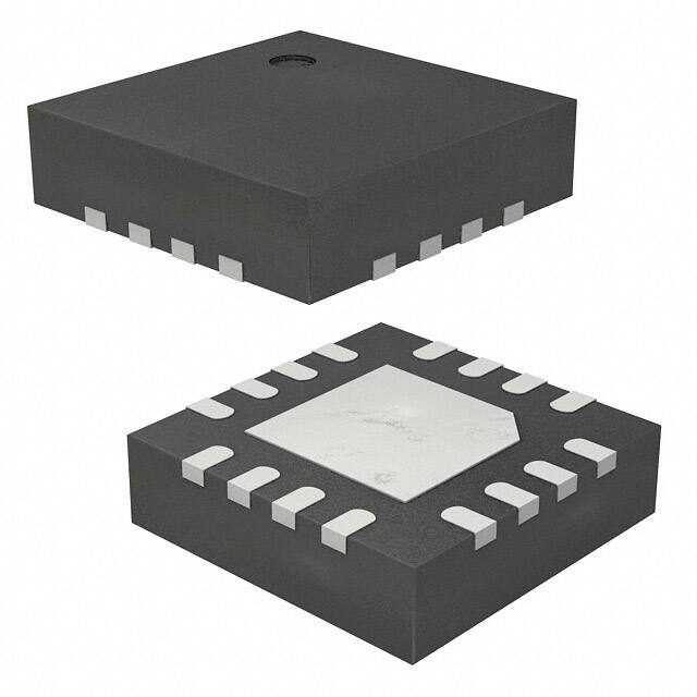
Very small QFN package is added to lineup. It is suitable for a small mounting and reduces the mounting area.
Features
Guarantee Nonlinearity error : +/-1.0LSB, Differential nonlinearity error : +/-0.7LSB
Data transfer format: 12-bit serial data input type by 3 wire ( DI, SCK, LD )
Output buffer op-amps: Operable over entire voltage range from almost ground to Vcc ( 0 to 5V )
Very small size package line-up: QFN-16(pin pitch: 0.5mm), TSSOP-16 (pin pitch 0.65mm)
Application
Conversion from digital data to analog control data for home-use and industrial equipment.
Signal gain control or automatic adjustment of LCD-TV, PDP-TV or LCD display-monitor.
Blurring correction control or various control of the interchangeable lens of digital still camera.
Automatic adjustment by combination with microcomputer and EEPROM.
(substitution of half fixed resistance)
Block Diagram
Number for TSSOP package
Number for QFN package
DI
4
2
CLK
3
1
12-bit shift register
D0 D1 D2 D3 D4 D5 D6 D7
Channel decoder
Vcc
16 14
16 2
LD
6
1
8
DO
1 2 3 4 5 6
8
Power on
reset
GND
15 1
D8 D9 D10 D11
6
6
8–bit latch
8-bit latch
8-bit upper
Segment R-2R
8-bit upper
Segment R-2R
7
3
4
9
10
11
12
13
9
5
6
11
12
13
14
15
VrefL
Ao1
Ao2
Ao3
Ao4
Ao5
Ao6
VrefU
R03DS0018EJ0100 Rev.1.00
2011.09.05
Page 1 of 8
�New Product
R2A20166NP/SA
Pin Arrangement
DI
2
Ao1
3
Ao2
4
14 Vcc
13 VrefU
R2A20166SA (Top view)
12 Ao6
Do 1
16 Vcc
LD 2
15 VrefU
CLK 3
11 Ao5
DI 4
10 Ao4
5
9
Ao3
Ao1
Ao2 6
NC 8
VrefL 7
GND 6
NC 5
N.C.
7
R2A20166SA
1
R2A20166NP
CLK
15 DO
16 LD
R2A20166NP (Top view)
GND 8
N.C. : Not connected
Outline: PWQN0016KB-A [NP]
14 Ao6
13 Ao5
12 Ao4
11 Ao3
10 N.C.
9
VrefL
N.C. : Not connected
Outline: PTSP0016JB-A [SA]
Pin Description
Pin No.
Symbol
Function
[QFN]
[TSSOP]
2
4
DI
1
3
CLK
Serial clock input terminal
(Input signal from DI terminal is input to 12-bit shift register at rise of
serial clock.)
16
2
LD
Load terminal
(When High level is input to LD terminal, value in 12-bit shift register
is loaded into decoder and 8-bit latch.)
15
1
Do
Serial data output terminal
(Data is sequentially output from the MSB bit.)
3
5
Ao1
4
6
Ao2
9
11
Ao3
10
12
Ao4
11
13
Ao5
12
14
Ao6
14
16
Vcc
6
8
GND
GND terminal
13
15
VrefU
D/A converter upper reference voltage input terminal
7
9
VrefL
D/A converter lower reference voltage input terminal
5
7
N.C.
Not connected
8
10
N.C.
Not connected
R03DS0018EJ0100 Rev.1.00
2011.09.05
Serial data input terminal.
( Input serial data with a 12-bit data length )
8-bit resolution D/A converter output terminals
(After power on, all channels are reset and DAC data 00h is output.)
Power supply terminal
Page 2 of 8
�New Product
R2A20166NP/SA
Absolute Maximum Ratings
Item
(Ta= +25deg unless otherwise noted)
Ratings
Unit
Supply voltage
Symbol
Vcc
Conditions
-0.3 to +6.5
V
D/A converter upper reference voltage
VrefU
-0.3 to +6.5
V
D/A converter lower reference voltage
VrefL
-0.3 to +6.5
V
Buffer amplifier output current
IAO
-2.0 to +2.0
mA
Input voltage
Vin
-0.3 to Vcc+0.3 VrefU, GND,VrefL =0V, Ta= -30 to +85deg, Unless otherwise noted )
Limits
Item
Symbol
Test conditions
Unit
Min
Typ
Max
2.7
5.0
5.5
V
Supply voltage
Vcc
Supply current
Icc
CLK = 1MHz, Vcc =5V, IAO =0µA
-
0.35
1.1
mA
Input leak current
IILK
VIN = 0 to Vcc
-10
-
10
µA
Input low voltage
VIL
-
-
0.2Vcc
V
4.0V < Vcc
0.5Vcc
-
-
V
Input high voltage
VIH
Vcc 4.0V
0.8Vcc
-
-
V
4.0V < Vcc, IOL = 2.0 mA
-
-
0.4
V
Vcc < 4.0V, IOL = 1.5 mA
-
-
0.4
V
VOL
Output low voltage
Output high voltage
VOH
IOH = -400 µA
Vcc – 0.4
-
-
V
Supply voltage
rise time *1
trVcc
Vcc = 0 to 2.7V
100
-
-
µs
VccPOR
Vcc = 0 to 2.7V
-
1.5
1.9
V
tPOR
Vcc < 0.1V
1
-
-
ms
Internal reset
operating voltage *1
Power supply restart
interval (Power supply
OFF ON)
*1
*1 : When power supply is turned on, internal circuit is initialized by power on reset circuit. But, if re-powered
on quickly, initialize is not operate. So, keep the time period of re-powered on (tPOR).
trVcc
Vcc
tPOR
(equivalent to trVcc)
VccPOR
GND
Internal
Reset signal
< 0.1V
GND
Resetting period
R03DS0018EJ0100 Rev.1.00
2011.09.05
Resetting period
Page 3 of 8
�New Product
R2A20166NP/SA
« Analog Part »
( Vcc, VrefU = +5V +/-10%, Vcc>VrefU, GND,VrefL =0V, Ta= -30 to +85deg, unless otherwise noted )
Limits
Item
Symbol
Unit
Test conditions
VrefU=5V, VrefL=0V, IAO=0µA,
Data condition: at maximum current
Min
Typ
Max
-
0.8
1.6
mA
Current dissipation
IrefU
D/A converter upper
reference voltage range *2
VrefU
0.7Vcc
-
Vcc
V
D/A converter lower
reference voltage range *2
VrefL
GND
-
0.3Vcc
V
Buffer amplifier output
voltage range
IAO = +/- 100 µA
0.1
-
Vcc – 0.1
V
VAO
IAO = +/- 500 µA
0.2
-
Vcc – 0.2
V
Buffer amplifier output
drive range
IAO
Upper side saturation voltage = 0.3V,
Lower side saturation voltage = 0.2V
-1.0
-
1.0
mA
Differential nonlinearity
SDL
-0.7
-
0.7
LSB
-1.0
-
1.0
LSB
-2.0
-
2.0
LSB
-2.0
-
2.0
LSB
Nonlinearity
SL
Zero code error
SZERO
Full scale error
SFULL
VrefU = 4.79V,
VrefL = 0.95V,
Vcc = 5.5V (15mV/LSB),
Without load (IAO =0µA)
Output capacitive load
Co
-
-
0.1
µF
Buffer amplifier output
impedance
Ro
-
5.0
-
ohm
*2 : The output does not necessary be the value with the reference voltage setting range.
The output value is determined by the buffer amplifier output voltage range (VAO).
R03DS0018EJ0100 Rev.1.00
2011.09.05
Page 4 of 8
�New Product
R2A20166NP/SA
AC Characteristics
( Vcc,VrefU = +5V+/-10%, Vcc VrefU, GND=VrefL = 0V, Ta = -30 to +85deg, unless otherwise noted )
Limits
Item
Symbol
Test conditions
Min
Typ
Max
Unit
Clock frequency
fCLK
-
1.0
10
MHz
Clock low pulse width
tCKL
40
-
-
ns
Clock high pulse width
tCKH
40
-
-
ns
Clock rise time
tCR
-
-
200
ns
Clock fall time
tCF
-
-
200
ns
Data setup time
tDCH
4
-
-
ns
Data hold time
tCHD
30
-
-
ns
LD setup time
tCHL
40
-
-
ns
LD hold time
tLDC
40
-
-
ns
LD high pulse width
tLDH
Data output delay time
tDO
CL < 100 pF
D/A output settling time
tLDD
Ta=25deg, CL
很抱歉,暂时无法提供与“R2A20168NP#W5”相匹配的价格&库存,您可以联系我们找货
免费人工找货