Datasheet
R2A30440NP
R19DS0063EJ0100
Rev.1.00
May 10, 2012
6-Channel Motor Driver IC for DSC, DVC and Surveillance Cameras
Overview
IN3/BF_IN
IN4/CPOUT2
CS
SCLK
SDAT
VM5
OUT5A
PGND5(RNF5)
OUT5B
PI3/BF_OUT/VDIN1
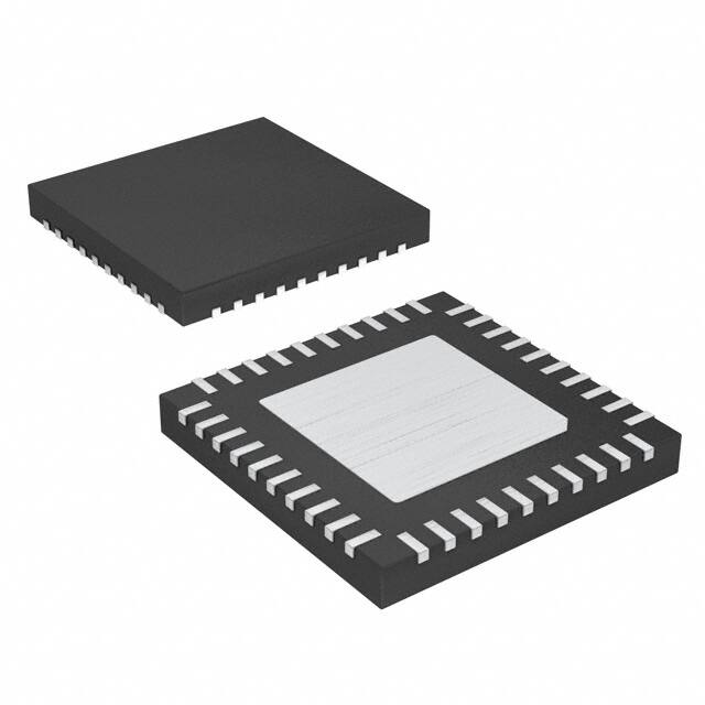
Pin Layout (Top View)
Package:40QFN
[5x5mm t=0.8mm(Max)]
The R2A30440NP is a semiconductor integrated circuit that incorporates
driver circuits suitable for motors in digital cameras.
The terminal arrangements are basically identical to that of R2A30423NP.
Features
CMOS process adoption and 1ch-4ch using D class amplifier to achieve low
power consumption.
A small 40-pin QFN package 5mm x 5mm, t=0.80mm (max) is used.
Built-in autonomous drive circuit controlled by serial settings (self propelled
control)
1ch/2ch and 3ch/4ch are capable of 2-2 phase stepper drive, 1-2 phase
(100%) stepper drive, 1-2 phase (70%) stepper drive and 256/512/1024
resolution micro-steps.
3ch/4ch is capable of constant voltage drive.
5ch is capable of constant current drive and FLL control.
6ch is capable of constant current drive.
By using exclusive control mode on 5ch and 6ch, it resembles 7ch drive.
Built-in 3 PI drivers channels
Built-in 2 comparators and 1 Schmitt buffer.
Built-in low-voltage malfunction prevention and thermal shutdown circuit.
Power supplies VCC and VM are internally isolated and include a function to
prevent reverse current between the power supplies.
30
31
21
20
VDIN2/PI2
OUT4B
PGND34
OUT4A
VM34
OUT3B
CPIN2
OUT3A
EXT2/ST2/CPOUT2
MOB2/CPOUT1
OSCIN
IN5
IN6
VM6
OUT6A
PGND6(RNF6)
OUT6B
RESET
VCC
PI1
1
Application
11
MOB1/SDO
EXT1/ST1
OUT2B
CPIN1
OUT2A
VM12
OUT1B
PGND12
OUT1A
DGND
40
10
Note)
The terminals (lead) are on the package underside.
At the Package central underside is a heat sink PAD.
Heat dissipation shield (and etc.) connection at DGND is
recommended.
Each VM pins respectively are not connected to each
other internally. Please connect them externally.
Motor driver for digital still cameras
Recommended operating conditions
Power-supply voltage range VCC: 2.7V~3.6V
VM: 2.7V~5.5V
Rated power-supply voltage VCC: 3.3V
VM: 5.0V
Block diagram and example of application circuit
U-STEP
Circuit
CP
Exclusive
Control 1
23
22
24
33
OUT2B
OUT1B
34
COIL
STM3
R19DS0063EJ0100 Rev.1.00
May 10, 2012
36
38
STM2
COIL
COIL
35
COIL
3
5
6
STM1
COIL
7
9
PGND12
OUT3B
32
OUT1A
1CH
D class amp
H-bridge
VM12
2CH
D class amp
H-bridge
OUT4A
3CH
D class amp
H-bridge
OUT4B
VM5
25
PGND34
OUT5A
OUT5B
PGND5
(RNF5)
17
STEP
4CH
D class amp
H-bridge
)
16
VM6
OUT6A
14
STEP
5CH
CC/FS
H-bridge
(
(
)
15
OUT6B
PGND6
(RNF6)
6CH
CC/FS
H-bridge
U-STEP
Circuit
OUT3A
DAC
10
DGND
8
10uF
0-2V DAC
4bit Comp
VM34
Comp
39
2
MCLK
1MHz
FLL
Controller
Latch
40
5MHz
OUT2A
CP
1
EXT2/ST2
/CPOUT2
Frequency
Divider
Serial Control Logic
DAC
20
EXT1/ST1
26
MOB/EXT
MOB2/CPOUT1
27
MOB1/SDO
28
OSCIN
13
SCLK
11
RESET
31
PI1
21
PI2
/VDIN2
30
PI3
/BFOUT
/VDIN1
29
IN3/BFIN
IN6
BIAS
Low voltage
detection
TSD
VREF(1.25V)
19
IN5
18
IN4/CPOUT2
CPIN2
37
U-STEP
FLL
Serial
Control Signal Reference clock
1MHz~27MHz
(3 lines)
CS
10uF
CPIN1
4
VCC
12
Reset
H: Active
L: Standby
Control Signal
(3,4,5,6CH)
SDAT
MCU
2.7~3.6V
VCC
power
supply
VM
Power
supply
FS : Full-swing
CV : Average Constant-Voltage
CC : Constant-Current
Page 1 of 6
�R2A30440NP
Absolute Maximum Ratings (Unless specified, the ambient temperature is 25C)
Item
Symbol
Rated Value
Unit
Power-supply voltage 1
VCC
6.5
V
Note1
Power-supply voltage 2
VM
6.5
V
Note1
Direct current (1ch~2ch)
Iod
600
mA/ch
Note4 DC
Instantaneous output current
(1ch~2ch)
Iop
800
mA/ch
Note4 PW < 10ms, Duty 20%
Direct current (3ch~6ch)
Iod
800
mA/ch
Note4 DC
Allowable power consumption
Pd
1590
mW
Note2 (Ta = 25C)
Thermal derating ratio
K
–12.72
mW/C
Note2 (Ta 25C)
Tj
150
C
Vin
–0.3~VCC+0.3
V
Ambient operating temperature
Topr
–30~85
C
Storage temperature
Tstg
–40~150
C
Max. junction temperature
Applied input voltages
Remarks
Note3
Notes: 1. As a rule, do not apply reverse power-supply voltages.
2. Glass epoxy board: 76.2mm x 114.5mm x 1.6mm,
copper-occupancy ratio in a 4-layer board: 20% in layers 1 and 4, 100% in layers 2 and 3.
Note that the allowable power consumption changes according to the conditions imposed on the board.
3. As a rule, do not apply voltages above the power-supply voltage or below the GND voltage.
4. The total output current does not exceed the rated value in usage with multiple channels simultaneously
turned on.
Thermal
Derating Curve
1590
Power consumption Pd [mW]
1500
–12.72mW/C
1000
826
500
0
20
60
80
100
120
40
Ambient operating temperature Ta [C]
140
160
[Remarks]
The electric power which the power consumption of this IC with the output transistor of 1ch - 6ch becomes dominant.
Output transistor power consumption formula
: (output current)2 x ON resistance
E.g. (500mA)2 x 2.0ohm=500mW
: output current x {VM – RNF5 – output current x RM}
Note: In constant current control, the on resistance is not included in the calculation
We recommend that you solder to connect the heatsink at the bottom of the package.
(To fix it to a potential, please connect with pin 10: DGND)
When the ambient temperature is 25C or more, refer to the above figure in selecting the required heat sink.
R19DS0063EJ0100 Rev.1.00
May 10, 2012
Page 2 of 6
�R2A30440NP
Terminal Function Explanation
I/O
Pin Function
MOB1/SDO
O
MOB1/SDO output
2
EXT1/ST1
O
EXT1/ST1 output
3
OUT2B
O
Channel 2 B output
4
CPIN1
I
Comparator 1 input
5
OUT2A
O
Channel 2 A output
6
VM12
7
OUT1B
8
PGND12
Power supply Motor power supply for channels 1, 2
O
GND
Channel 1 B output
Motor power GND for channels 1, 2
9
OUT1A
O
10
DGND
GND
11
PI1
12
VCC
13
RESET
I
Internal logic reset
14
OUT6B
O
Channel 6 B output
15
PGND6(RNF6)
O
Channel 1 A output
Control GND
PI driver output
Power supply Control power supply
GND
O
OUT6A
17
VM6
Channel 6 A output
18
IN6
I
19
IN4
I/O
20
OSCIN
21
PI3/BF_OUT
/VDIN1
22
OUT5B
23
PGND5(RNF5)
24
OUT5A
25
VM5
26
SDAT
I
Serial control signal
27
SCLK
I
Serial control signal
28
CS
I
Serial control signal
29
IN4
I
Channels 3, 4, 5, 6 control
30
IN3/BF_IN
I
Channels 3, 5 control/Buffer input
31
PI2/VDIN2
I/O
PI driver output/ VD signal input 2
32
OUT4B
O
Channel 4 B output
33
PGND34
34
OUT4A
35
VM34
36
OUT3B
O
Channel 3 B output
37
CPIN2
I
Comparator 2 input
38
OUT3A
O
Channel 3 A output
39
EXT2/ST2
/CPOUT2
O
EXT2/ST2 output
/Comparator 2 output
40
MOB2
/CPOUT1
O
MOB2 output
/Comparator 1 output
Power supply Motor power supply for channel 6
OSCIN
IN5
IN6
VM6
OUT6A
PGND6(RNF6)
OUT6B
RESET
VCC
PI1
VDIN2/PI2
OUT4B
PGND34
OUT4A
VM34
OUT3B
CPIN2
OUT3A
EXT2/ST2/CPOUT2
MOB2/CPOUT1
40
1
20
11
10
Channels 4, 5, 6 control
/Comparator 2 output
Clock
PI driver output/Buffer Output
/VD signal input 1
O
Channel 5 B output
O
31
21
Channels 5, 6 control
I/O
GND
30
Motor power GND for channel 6
16
I
Pin Layout (Top View)
Package:40QFN
[5x5mm t=0.8mm(Max)]
IN3/BF_IN
IN4/CPOUT2
CS
SCLK
SDAT
VM5
OUT5A
PGND5(RNF5)
OUT5B
PI3/BF_OUT/VDIN1
Pin Name
1
MOB1/SDO
EXT1/ST1
OUT2B
CPIN1
OUT2A
VM12
OUT1B
PGND12
OUT1A
DGND
Pin No.
Motor power GND for channel 5
Channel 5 A output
Power supply Motor power supply for channel 5
GND
O
Motor power GND for channels 3, 4
Channel 4 A output
Power supply Motor power supply for channels 3, 4
R19DS0063EJ0100 Rev.1.00
May 10, 2012
Page 3 of 6
�R2A30440NP
Actuator connection pattern(1)
[Connection pattern 1]
1ch
CC/FS
STM1
u-STEP
3ch
4ch
STM2
5ch
6ch
CC/FS
CC/FS
1line control
1line
Serial
Serial
(IN3 or IN4 or IN5) control
autonomous autonomous
or
(IN6)
2line control
control
control
or
(IN3/IN4)
(IN3/IN5)
2line
(IN4/IN5)
control
or
(IN5/IN6)
Serial
or
serial
(automatic PWM)
or
1line control
(IN3or IN4 or IN5)
CC/FS
STM2
2ch
STM1
OUT1A
OUT1B
OUT2A
OUT2B
VM12
OUT3A
OUT3B
OUT4A
VM34
OUT4B
OUT5A
VM5
OUT5B
OUT6A
OUT6B
VM6
u-STEP
FLL control
serial+1line
(IN3 or IN4 or IN5)
The control method of each CH is set through serial.
5ch FLL control/ automatic PWM control is only valid after FS mode is selected.
[Connection pattern 2]
1ch
OUT1A
OUT1B
OUT2A
VM12
OUT2B
OUT3A
OUT3B
OUT4A
VM34
OUT4B
OUT5A
VM5
OUT5B
OUT6A
OUT6B
VM6
2ch
STM1
3ch
4ch
5ch
STM2
Serial
Serial
autonomous autonomous
control
control
6ch
STM3
CC/FS
3line control
(IN4/IN5/IN6)
or
(IN3/IN5/IN6)
STM3
1-2 phase(100%)
2-2 phase
STM2
STM1
u-STEP
u-STEP
The control method of each CH is
set through serial.
[Connection pattern 3]
CC/FS
CC/FS
STM2
STM1
u-STEP
u-STEP
2ch
STM1
OUT1A
OUT1B
OUT2A
VM12
OUT2B
OUT3A
OUT3B
OUT4A
VM34
OUT4B
OUT5A
OUT5B
OUT6A
OUT6B
CC/FS
1ch
VM5
VM6
3ch
4ch
STM2
6ch
7ch
CC/FS
CC/FS
1line control
1line
(IN3 or IN4 or IN5)
Serial
Serial
control
or
autonomous autonomous
(IN6)
2line control
control
control
(IN3/IN4)
or
(IN3/IN5)
2line
(IN4/IN5)
control
or
(IN5/IN6)
serial
or
serial (automatic
PWM)
or
1line control
(IN3or IN4 or IN5)
Exclusive control
Serial
FLL control
serial+1line
(IN3 or IN4 or IN5)
The control method of each CH is set through serial.
5ch FLL control/ automatic PWM control is only valid after
FS mode is selected.
R19DS0063EJ0100 Rev.1.00
May 10, 2012
5ch
CC/FS
Exclusive Control
5ch,6ch,7ch cannot be simultaneously operated.
Only one channel is operated at a time.
Page 4 of 6
�R2A30440NP
Actuator connection pattern(2)
1ch
[Connection pattern 4]
CC/FS
Serial
autonomous
control
CV
CV
3ch
4ch
5ch
6ch
CV
CV
CC/FS
CC/FS
OUT1A
OUT1B
OUT2A
VM12
OUT2B
OUT3A
OUT3B
OUT4A
VM34
OUT4B
OUT5B
OUT6A
OUT6B
CC/FS
OUT5A
VM5
VM6
2ch
STM1
STM1
u-STEP
1line
control
(IN3
or IN4
or IN5)
or
serial
1line
control
(IN3
or IN4
or IN5)
or
serial
1line control
(IN3 or IN4 or IN5)
or
2line control
(IN3/IN4)
(IN3/IN5)
1line
(IN4/IN5)
control
or
(IN6)
serial
or
or
serial (automatic
2 line
PWM)
control
or
(IN5/IN6)
1 line control
(IN3or IN4 or IN5)
FLL control
serial +1line
(IN3 or IN4 or IN5)
The control method of each CH is set through serial.
5ch FLL/automatic PWM control is only valid after FS mode is selected.
For CH3 & CH4 CV, the output is from a D-class amplifier and therefore
the output is full swing PWM.
[Connection pattern 5]
CV
STM3
1ch
OUT1A
OUT1B
OUT2A
VM12
OUT2B
OUT3A
OUT3B
OUT4A
VM34
OUT4B
OUT5B
OUT6A
OUT6B
OUT5A
VM5
VM6
CV
STM1
1-2 phase(100%)
2-2 phase
CV
STM1
4ch
5ch
CV
1line
1line
Serial
control
control
autonomous (IN3or IN4 (IN3or IN4
control
or IN5)
or IN5)
or
or
serial
serial
6ch
STM3
CC/FS
3line control
(IN4/IN5/IN6)
or
(IN3/IN5/IN6)
The control method of each CH is set through serial.
For CH3 & CH4 CV, the output is from a D-class amplifier and
therefore the output is full swing PWM.
1ch
CC/FS
CV
CV
STM1
u-STEP
CC/FS
2ch
STM1
OUT1A
OUT1B
OUT2A
VM12
OUT2B
OUT3A
OUT3B
OUT4A
VM34
OUT4B
OUT5A
VM5
OUT5B
OUT6A
OUT6B
CC/FS
3ch
u-STEP
[Connection pattern 6]
VM6
2ch
3ch
4ch
5ch
6ch
7ch
CV
CV
CC/FS
CC/FS
CC/FS
1line control
(IN3 or IN4 or IN5)
or
2line control
(IN3/IN4)
(IN3/IN5)
1line
1line
1line
(IN4/IN5)
Serial
control
control
control
or
autonomous (IN3or IN4 (IN3or IN4
(IN6)
serial
control
or
or IN5)
or
or IN5)
Serial (automatic
or
2line
or
PWM)
serial
control
serial
or
(IN5/IN6)
1line control
(IN3or IN4 or IN5)
Exclusive control
Serial
FLL control
serial +1line
(IN3 or IN4 or IN5)
The control method of each CH is set through serial.
5ch FLL/automatic PWM control is only valid after FS mode is selected.
For CH3 & CH4 CV, the output is from a D-class amplifier
and therefore the output is full swing PWM.
R19DS0063EJ0100 Rev.1.00
May 10, 2012
Exclusive Control
5ch,6ch,7ch cannot be simultaneously operated.
Only one channel is operated at a time.
Page 5 of 6
�R2A30440NP
Package Dimensions
Ordering Information
Orderable Part No.
Package Code
Quantity
R2A30440NP#W0
PWQN0040LD-A
5000 pcs
R2A30440NP#U0
PWQN0040LD-A
1 pc
R19DS0063EJ0100 Rev.1.00
May 10, 2012
Page 6 of 6
�Notice
1.
Descriptions of circuits, software and other related information in this document are provided only to illustrate the operation of semiconductor products and application examples. You are fully responsible for
the incorporation of these circuits, software, and information in the design of your equipment. Renesas Electronics assumes no responsibility for any losses incurred by you or third parties arising from the
use of these circuits, software, or information.
2.
Renesas Electronics has used reasonable care in preparing the information included in this document, but Renesas Electronics does not warrant that such information is error free. Renesas Electronics
3.
Renesas Electronics does not assume any liability for infringement of patents, copyrights, or other intellectual property rights of third parties by or arising from the use of Renesas Electronics products or
assumes no liability whatsoever for any damages incurred by you resulting from errors in or omissions from the information included herein.
technical information described in this document. No license, express, implied or otherwise, is granted hereby under any patents, copyrights or other intellectual property rights of Renesas Electronics or
others.
4.
You should not alter, modify, copy, or otherwise misappropriate any Renesas Electronics product, whether in whole or in part. Renesas Electronics assumes no responsibility for any losses incurred by you or
5.
Renesas Electronics products are classified according to the following two quality grades: "Standard" and "High Quality". The recommended applications for each Renesas Electronics product depends on
third parties arising from such alteration, modification, copy or otherwise misappropriation of Renesas Electronics product.
the product's quality grade, as indicated below.
"Standard": Computers; office equipment; communications equipment; test and measurement equipment; audio and visual equipment; home electronic appliances; machine tools; personal electronic
equipment; and industrial robots etc.
"High Quality": Transportation equipment (automobiles, trains, ships, etc.); traffic control systems; anti-disaster systems; anti-crime systems; and safety equipment etc.
Renesas Electronics products are neither intended nor authorized for use in products or systems that may pose a direct threat to human life or bodily injury (artificial life support devices or systems, surgical
implantations etc.), or may cause serious property damages (nuclear reactor control systems, military equipment etc.). You must check the quality grade of each Renesas Electronics product before using it
in a particular application. You may not use any Renesas Electronics product for any application for which it is not intended. Renesas Electronics shall not be in any way liable for any damages or losses
incurred by you or third parties arising from the use of any Renesas Electronics product for which the product is not intended by Renesas Electronics.
6.
You should use the Renesas Electronics products described in this document within the range specified by Renesas Electronics, especially with respect to the maximum rating, operating supply voltage
range, movement power voltage range, heat radiation characteristics, installation and other product characteristics. Renesas Electronics shall have no liability for malfunctions or damages arising out of the
use of Renesas Electronics products beyond such specified ranges.
7.
Although Renesas Electronics endeavors to improve the quality and reliability of its products, semiconductor products have specific characteristics such as the occurrence of failure at a certain rate and
malfunctions under certain use conditions. Further, Renesas Electronics products are not subject to radiation resistance design. Please be sure to implement safety measures to guard them against the
possibility of physical injury, and injury or damage caused by fire in the event of the failure of a Renesas Electronics product, such as safety design for hardware and software including but not limited to
redundancy, fire control and malfunction prevention, appropriate treatment for aging degradation or any other appropriate measures. Because the evaluation of microcomputer software alone is very difficult,
please evaluate the safety of the final products or systems manufactured by you.
8.
Please contact a Renesas Electronics sales office for details as to environmental matters such as the environmental compatibility of each Renesas Electronics product. Please use Renesas Electronics
products in compliance with all applicable laws and regulations that regulate the inclusion or use of controlled substances, including without limitation, the EU RoHS Directive. Renesas Electronics assumes
no liability for damages or losses occurring as a result of your noncompliance with applicable laws and regulations.
9.
Renesas Electronics products and technology may not be used for or incorporated into any products or systems whose manufacture, use, or sale is prohibited under any applicable domestic or foreign laws or
regulations. You should not use Renesas Electronics products or technology described in this document for any purpose relating to military applications or use by the military, including but not limited to the
development of weapons of mass destruction. When exporting the Renesas Electronics products or technology described in this document, you should comply with the applicable export control laws and
regulations and follow the procedures required by such laws and regulations.
10. It is the responsibility of the buyer or distributor of Renesas Electronics products, who distributes, disposes of, or otherwise places the product with a third party, to notify such third party in advance of the
contents and conditions set forth in this document, Renesas Electronics assumes no responsibility for any losses incurred by you or third parties as a result of unauthorized use of Renesas Electronics
products.
11. This document may not be reproduced or duplicated in any form, in whole or in part, without prior written consent of Renesas Electronics.
12. Please contact a Renesas Electronics sales office if you have any questions regarding the information contained in this document or Renesas Electronics products, or if you have any other inquiries.
(Note 1)
"Renesas Electronics" as used in this document means Renesas Electronics Corporation and also includes its majority-owned subsidiaries.
(Note 2)
"Renesas Electronics product(s)" means any product developed or manufactured by or for Renesas Electronics.
http://www.renesas.com
SALES OFFICES
Refer to "http://www.renesas.com/" for the latest and detailed information.
Renesas Electronics America Inc.
2880 Scott Boulevard Santa Clara, CA 95050-2554, U.S.A.
Tel: +1-408-588-6000, Fax: +1-408-588-6130
Renesas Electronics Canada Limited
1101 Nicholson Road, Newmarket, Ontario L3Y 9C3, Canada
Tel: +1-905-898-5441, Fax: +1-905-898-3220
Renesas Electronics Europe Limited
Dukes Meadow, Millboard Road, Bourne End, Buckinghamshire, SL8 5FH, U.K
Tel: +44-1628-651-700, Fax: +44-1628-651-804
Renesas Electronics Europe GmbH
Arcadiastrasse 10, 40472 Düsseldorf, Germany
Tel: +49-211-65030, Fax: +49-211-6503-1327
Renesas Electronics (China) Co., Ltd.
7th Floor, Quantum Plaza, No.27 ZhiChunLu Haidian District, Beijing 100083, P.R.China
Tel: +86-10-8235-1155, Fax: +86-10-8235-7679
Renesas Electronics (Shanghai) Co., Ltd.
Unit 204, 205, AZIA Center, No.1233 Lujiazui Ring Rd., Pudong District, Shanghai 200120, China
Tel: +86-21-5877-1818, Fax: +86-21-6887-7858 / -7898
Renesas Electronics Hong Kong Limited
Unit 1601-1613, 16/F., Tower 2, Grand Century Place, 193 Prince Edward Road West, Mongkok, Kowloon, Hong Kong
Tel: +852-2886-9318, Fax: +852 2886-9022/9044
Renesas Electronics Taiwan Co., Ltd.
13F, No. 363, Fu Shing North Road, Taipei, Taiwan
Tel: +886-2-8175-9600, Fax: +886 2-8175-9670
Renesas Electronics Singapore Pte. Ltd.
80 Bendemeer Road, Unit #06-02 Hyflux Innovation Centre Singapore 339949
Tel: +65-6213-0200, Fax: +65-6213-0300
Renesas Electronics Malaysia Sdn.Bhd.
Unit 906, Block B, Menara Amcorp, Amcorp Trade Centre, No. 18, Jln Persiaran Barat, 46050 Petaling Jaya, Selangor Darul Ehsan, Malaysia
Tel: +60-3-7955-9390, Fax: +60-3-7955-9510
Renesas Electronics Korea Co., Ltd.
11F., Samik Lavied' or Bldg., 720-2 Yeoksam-Dong, Kangnam-Ku, Seoul 135-080, Korea
Tel: +82-2-558-3737, Fax: +82-2-558-5141
© 2012 Renesas Electronics Corporation. All rights reserved.
Colophon 2.2
�


 工商网监
湘ICP备2023018690号
工商网监
湘ICP备2023018690号
