Datasheet
RL78/H1D
R01DS0318EJ0100
Rev. 1.00
Apr 13, 2018
RENESAS MCU
Analog front-end (24-bit ΔΣA/D converter with programmable gain instrumentation amplifier, Amplifier
unit and 12-bit D/A converter), External signal sampler/Sampling output timer detector and Integrated
LCD controller/driver.
True Low Power Platform (as low as 70.8 μA/MHz, and 0.68 μA in Halt mode( RTC2 + LVD)), 1.8 V to
5.5V operation, 64 to 128 Kbyte Flash, 33 DMIPS at 24 MHz, for Healthcare and Flow meter
applications.
1. OUTLINE
1.1
Features
Ultra-low power consumption technology
can be executed from the program memory
• VDD = 2.4 to 5.5 V
(10-bit SAR A/D converter: 2.4 to 5.5 V,
operating voltage of the analog front-end
(AFE): 2.7 to 5.5 V)
• Background operation (BGO): Instructions
Note 1,
VDD = 1.8 to 5.5 VNote 2
• HALT mode
• STOP mode
• SNOOZE mode
RL78 CPU core
• CISC architecture with 3-stage pipeline
• Minimum instruction execution time: Can be
changed from high speed (0.04167 µs: @ 24
while rewriting the data flash memory.
• Number of rewrites: 1,000,000 times (TYP.)
• Voltage of rewrites: VDD = 2.4 to 5.5 VNote 1,
1.8 to 5.5 VNote 2
High-speed on-chip oscillator
• Select from 24 MHz, 16 MHz, 12 MHz, 8
MHz, 6 MHz, 4 MHz, 3 MHz, 2 MHz, and 1
MHz
• High accuracy: ±1.0% (VDD = 2.4 to 5.5 V, TA
= -20 to +85°CNote 1, VDD = 1.8 to 5.5 V, TA =
-20 to +85°CNote 2)
MHz operation with high-speed on-chip
oscillator clock) to ultra-low speed (30.5 µs:
@ 32.768 kHz operation with subsystem
clock)
• Multiply/divide and multiply/accumulate
Operating ambient temperature
• TA = -40 to +85°C (A: Consumer
applicationsNote 1, D: Industrial
applicationsNote 2)
instructions are supported.
• Address space: 1 MB
• General-purpose registers: (8-bit register × 8)
× 4 banks
• On-chip RAM: 5.5 KBNote 1, 8 KBNote 2
Power management and reset function
• On-chip power-on-reset (POR) circuit
• On-chip voltage detector (LVD) (Select
interrupt and reset from 9Note 1 or 12Note 2
levels)
Code flash memory
• Code flash memory: 64 to 128 KB
• Block size: 1 KB
• Prohibition of block erase and rewriting
(security function)
• On-chip debug function
• Self-programming (with boot swap
Data transfer controller (DTC)
• Transfer modes: Normal transfer mode,
repeat transfer mode, block transfer mode
• Activation sources: Activated by interrupt
sources (35 sources).
• Chain transfer function
function/flash shield window function)
Event link controller (ELC)
Data flash memory
• Data flash memory: 4 KB
R01DS0318EJ0100 Rev. 1.00
Apr 13, 2018
• Event signals of 18 to 26 types can be linked
to the specified peripheral function.
Page 1 of 143
�RL78/H1D
1. OUTLINE
Serial interfaces
• CSI/CSI (SPI supported): 3 channels
• UART/UART (LIN-bus supported):3 channels
• I2C/simplified I2C: 4 channels
• Serial interface UARTMG (9600 bps @ 38.4
kHz): 1 channel (R5F11R only)
Timers
• 16-bit timer:
Timer array unit (TAU): 8 channels,
Timer RJ: 2 channels (R5F11R only)
• 8-bit timer:2 channelsNote 1, 6 channelsNote 2
• 12-bit interval timer: 1 channel
• Real-time clock 2: 1 channel (calendar for 99
years, alarm function, and clock correction
function)
• Watchdog timer: 1 channel (operable with the
dedicated low-speed on-chip oscillator)
• External signal sampler: 1 channel (R5F11R
only)
• Sampling output timer detector (SMOTD):
6 channels for input, 3 channels for output
(R5F11R only)
LCD controller/driver
• Internal voltage boosting method, capacitor
split method, and external resistance division
method are switchable.
• Segment signal output:
27 (23) to 36 (32) Note 3
• Common signal output: 4 (8)
Amplifier unit (R5F11N and R5F11P only)
• Programmable gain instrumentation amplifier
(PGA1): 1 channel (R5F11NL, R5F11PL, and
R5F11NG only)
- Analog input: 1 or 2 channels
- Variable gain: x12, x16, x20, x24
• Rail-to-rail operational amplifier (AMP0): 1
channel
• General-purpose operational amplifier
(AMP1, AMP2): 2 channels (R5F11NL,
R5F11PL, and R5F11NG only)
D/A converter (R5F11N and R5F11P only)
• 8-bit resolution R-2R resistor ladder D/A
converter (DAC0) (AVDD = 2.7 to 5.5 V):
1 channel
• 12-bit resolution R-2R resistor ladder D/A
converter (DAC1) (AVDD = 2.7 to 5.5 V):
1 channel (R5F11NL, R5F11PL, and
R5F11NG only)
10-bit SAR A/D converter
• 10-bit resolution A/D converter (VDD = 2.4 to
5.5 VNote 1, VDD = 1.8 to 5.5 VNote 2)
• Analog input: 3 channels
• Internal reference voltage (TYP. 1.45 V) Note 4
and temperature sensor Note 4
Note 3
Analog front-end power supply circuit
(R5F11N and R5F11P only)
• AFE reference power supply (ABGR)
• LDO for supplying power to internal circuits
(REGA)
• LDO for supplying power to a sensor
(SBIAS): 0.5 to 2.2 V
24-bit ΔΣ A/D converter with programmable gain
instrumentation amplifier (R5F11N and R5F11P
only)
• 24-bit second-order ΔΣ A/D converter (AVDD
= 2.7 to 5.5 V)
- SNDR: 85 dB (TYP.)
- Output data rate: 488 sps to 15.625 ksps in
normal mode
61 sps to 1.953 ksps in low power mode
• Programmable gain instrumentation amplifier
(PGA0)
- Analog input: 1 to 5 channels (differential
input mode or single-ended input mode)
R01DS0318EJ0100 Rev. 1.00
Apr 13, 2018
- D/A converter for offset adjustment
- Variable gain: x1 to x64
I/O ports
• I/O ports: 29 to 63 (N-ch open drain I/O
[withstand voltage of 6 V]: 2)
• Can be set to N-ch open drain, TTL input
buffer, and on-chip pull-up resistor
• On-chip clock output/buzzer output controller
Others
• On-chip BCD (binary-coded decimal)
correction circuit
Note 1.
Note 2.
Note 3.
Note 4.
Remark
In case of R5F11N and R5F11P.
In case of R5F11R.
The number in parentheses indicates
the number of signal outputs when 8
coms are used.
Selectable only in HS (high-speed
main) mode.
The functions mounted depend on the
product. See 1.6 Outline of Functions.
Page 2 of 143
�RL78/H1D
1. OUTLINE
ROM, RAM capacities
Flash ROM
Data Flash
RAM
128 KB
4 KB
96 KB
RL78/H1D
80-pin LFQFP
64-pin LFQFP
64-pin TFBGA
48-pin LFQFP
5.5 KB
R5F11NMG
R5F11NLG
R5F11PLG
R5F11NGG
4 KB
5.5 KB
R5F11NMF
R5F11NLF
R5F11PLF
R5F11NGF
64 KB
4 KB
5.5 KB
R5F11NME
—
—
—
128 KB
4 KB
8 KB
R5F11RMG
—
—
—
R01DS0318EJ0100 Rev. 1.00
Apr 13, 2018
Page 3 of 143
�RL78/H1D
1.2
Pin
Count
80 pins
1. OUTLINE
Ordering Information
Package
80-pin plastic LFQFP
Fields of
Application
A
(12 × 12 mm, 0.5 mm pitch)
64 pins
64-pin plastic LFQFP
64-pin plastic TFBGA
A
48-pin plastic LFQFP
A
80-pin plastic LFQFP
R5F11PLGABG#U0, R5F11PLFABG#U0
R5F11PLGABG#W0, R5F11PLFABG#W0
A
(7 × 7 mm, 0.5 mm pitch)
80 pins
R5F11NLGAFB#30, R5F11NLFAFB#30
R5F11NLGAFB#50, R5F11NLFAFB#50
(4 × 4 mm, 0.4 mm pitch)
48 pins
R5F11NMGAFB#30, R5F11NMFAFB#30, R5F11NMEAFB#30
R5F11NMGAFB#50, R5F11NMFAFB#50, R5F11NMEAFB#50
(10 × 10 mm, 0.5 mm pitch)
64 pins
Orderable Part Number
R5F11NGGAFB#30, R5F11NGFAFB#30
R5F11NGGAFB#50, R5F11NGFAFB#50
D
R5F11RMGDFB#30, R5F11RMGDFB#50
(12 × 12 mm, 0.5 mm pitch)
Remark
Products (R5F11PL) in 64-pin TFBGA have the same functionality as those (R5F11NG) in 48-pin LFQFP. The only
difference is the package.
R01DS0318EJ0100 Rev. 1.00
Apr 13, 2018
Page 4 of 143
�RL78/H1D
1. OUTLINE
Figure 1 - 1 Part Number, Memory Size, and Package of RL78/H1D
Part No. R 5 F 1 1 N M G A x x x F B # 3 0
Packaging specification:
#30: Tray (LFQFP)
#50: Embossed Tape (LFQFP)
#U0: Tray (TFBGA)
#W0: Embossed Tape (TFBGA)
Package type:
FB: LFQFP, 0.50 mm pitch
BG: TFBGA, 0.40 mm pitch
ROM number (Omitted with blank products)
Fields of application:
A: Consumer applications, TA = -40 to +85°C
D: Industrial applications, TA = -40 to +85°C
ROM capacity:
E: 64 KB
F: 96 KB
G: 128 KB
Pin count:
G: 48-pin
L: 64-pin
M: 80-pin
RL78/H1D group
11N: AFE incorporated, LFQFP package
11P: AFE incorporated, TFBGA package
11R: External signal sampler and SMOTD incorporated
Memory type:
F: Flash memory
Renesas MCU
Renesas semiconductor product
Caution
Orderable part numbers are current as of when this manual was published.
Please make sure to refer to the relevant product page on the Renesas website for the latest part numbers.
R01DS0318EJ0100 Rev. 1.00
Apr 13, 2018
Page 5 of 143
�RL78/H1D
1.3
1. OUTLINE
Pin Configuration (Top View)
1.3.1
80-pin products (R5F11NM)
COM5/SEG1
COM6/SEG2
COM7/SEG3
P53/(INTP0)/SEG4
P52/SCK10/SCL10/TI02/TO02/SEG5
P51/SI10/RxD1/SDA10/TI04/TO04/SEG6
P50/SO10/TxD1/TI03/TO03/SEG7
COM0
COM1
COM2
COM3
COM4/SEG0
P10/INTP2/SCK20/SCL20/SEG29
P07/SI20/RxD2/SDA20/TI05/TO05/SEG28
P06/SO20/TxD2/TI00/SEG27
P05/TI06/TO06/SEG26
P04/INTP6/(SCK10/SCL10)/SEG25
P03/(SI10/RxD1/SDA10)/TO00/SEG24
P02/(SO10/TxD1)/PCLBUZ0/SEG23
P01/(INTP5)/SEG22
• 80-pin plastic LFQFP (12 × 12 mm, 0.5 mm pitch)
60 59 58 57 56 55 54 53 52 51 50 49 48 47 46 45 44 43 42 41
P11/SEG30
P12/SEG31
P13/SEG32
P14/SEG33
P15/SEG34
P16/SEG35
P17/(TI07/TO07)
P84/(TI05/TO05)
P85/INTP7
P86/(INTP6)
ANI12
ANI13
ANI14
AVSS
AMP0O
AMP0N/AMP0P
AMP0P
PGA00P
PGA00N
SBIAS
61
62
63
64
65
66
67
68
69
70
71
72
73
74
75
76
77
78
79
80
RL78/H1D
(Top View)
40
39
38
37
36
35
34
33
32
31
30
29
28
27
26
25
24
23
22
21
P70/SEG8
P71/SEG9
P72/SEG10
P73/SEG11
P74/SEG12
P75/SEG13
P76/SEG14
P77/TI07/TO07/SEG15
P30/INTP3/RTC1HZ/SEG16
P31/TI01/TO01/SEG17
P32/INTP4/SSI00/SEG18
P35/SCK00/SCL00/SEG19
P36/SI00/RxD0/TOOLRxD/SDA00/PCLBUZ1/SEG20
P37/SO00/TxD0/TOOLTxD/SEG21
P125/(TI06/TO06)/VL3
VL4
VL2
VL1
P126/(TI05/TO05)/CAPL
P127/(TI04/TO04)/CAPH
RESET
P124/XT2/EXCLKS
P123/XT1
P137/INTP0/(SSI00)
P122/X2/EXCLK/INTP5
P121/X1/INTP1
REGC
VSS
VDD
P60/(INTP3)/SCLA0
P61/(INTP4)/SDAA0
REGA
AVDD
P80/(SO20/TxD2)/(TI02/TO02)
P81/(SI20/RxD2/SDA20)/(TI00)/(TO00)
P82/(INTP2)/(SCK20/SCL20)/(TI07/TO07)
P83/(TI03/TO03)/(PCLBUZ1)
P44/(SO00/TxD0)
P43/(SI00/RxD0/SDA00)/(TI00)/(TO00)
P40/TOOL0/(INTP1)/(SCK00/SCL00)/(TI01/TO01)
1 2 3 4 5 6 7 8 9 10 11 12 13 14 15 16 17 18 19 20
Caution 1. Connect the REGC pin to VSS pin via a capacitor (0.47 to 1 µF).
Caution 2. Connect the REGA pin to AVSS pin via a capacitor (0.22 μF).
Caution 3. Make the AVSS pin the same potential as the VSS pin.
Caution 4. Make the AVDD pin the same potential as the VDD pin.
Caution 5. Connect the SBIAS pin to AVSS pin via a capacitor (0.22 µF).
Remark 1. For pin identification, see 1.4 Pin Identification.
Remark 2. Functions in parentheses in the above figure can be assigned via settings in the peripheral I/O redirection registers 0 to 3
(PIOR0 to PIOR3).
Remark 3. Set the AMP0P and AMP0N functions in the above figure by the amplifier unit 1 input select register (AMP0S).
R01DS0318EJ0100 Rev. 1.00
Apr 13, 2018
Page 6 of 143
�RL78/H1D
1.3.2
1. OUTLINE
64-pin products (R5F11NL)
P10/INTP2/SCK20/SCL20/SEG29
P07/SI20/RxD2/SDA20/TI05/TO05/SEG28
P06/SO20/TxD2/TI00/SEG27
P05/ANI10/TI06/TO06/SEG26
P03/ANI8/TO00/SEG24
COM0
COM1
COM2
COM3
COM4/SEG0
COM5/SEG1
COM6/SEG2
COM7/SEG3
P52/SCK10/SCL10/TI02/TO02/SEG5
P51/SI10/RxD1/SDA10/TI04/TO04/SEG6
P50/SO10/TxD1/TI03/TO03/SEG7
• 64-pin plastic LFQFP (10 × 10 mm, 0.5 mm pitch)
48 47 46 45 44 43 42 41 40 39 38 37 36 35 34 33
49
32
50
31
51
30
52
29
53
28
54
27
55
26
56
25
57
24
58
23
59
22
60
21
61
20
62
19
63
18
64
17
1 2 3 4 5 6 7 8 9 10 11 12 13 14 15 16
RL78/H1D
(Top View)
P70/SEG8
P71/SEG9
P76/SEG14
P77/TI07/TO07/SEG15
P30/INTP3/RTC1HZ/SEG16
P31/TI01/TO01/SEG17
P32/INTP4/SSI00/SEG18
P35/SCK00/SCL00/SEG19
P36/SI00/RxD0/TOOLRxD/SDA00/PCLBUZ1/SEG20
P37/SO00/TxD0/TOOLTxD/SEG21
P125/(TI06/TO06)/VL3
VL4
VL2
VL1
P126/(TI05/TO05)/CAPL
P127/(TI04/TO04)/CAPH
REGA
AVDD
P82/(TI07/TO07)
P83/(TI03/TO03)/(PCLBUZ1)
P40/TOOL0/(INTP1)/(TI01/TO01)
RESET
P124/XT2/EXCLKS
P123/XT1
P137/INTP0
P122/X2/EXCLK/INTP5
P121/X1/INTP1
REGC
VSS
VDD
P60/(INTP3)/SCLA0
P61/(INTP4)/SDAA0
P11/ANI11/SEG30
P12/SEG31
P13/SEG32
P14/SEG33
P15/SEG34
AMP2O
AMP2N/AMP2P/AMP1P
AMP1O
AMP1N/AMP1P/AMP0P
PGA1O
AVSS
AMP0O
AMP0N/AMP0P
PGA10P/PGA00P/AMP1P
PGA10N/PGA00N/AMP2P
SBIAS
Caution 1. Connect the REGC pin to VSS pin via a capacitor (0.47 to 1 µF).
Caution 2. Connect the REGA pin to AVSS pin via a capacitor (0.22 μF).
Caution 3. Make the AVSS pin the same potential as the VSS pin.
Caution 4. Make the AVDD pin the same potential as the VDD pin.
Caution 5. Connect the SBIAS pin to AVSS pin via a capacitor (0.22 µF).
Remark 1. For pin identification, see 1.4 Pin Identification.
Remark 2. Functions in parentheses in the above figure can be assigned via settings in the peripheral I/O redirection registers 0 to 3
(PIOR0 to PIOR3).
Remark 3. Set the AMP0P and AMP0N functions in the above figure by the amplifier unit 1 input select register (AMP0S).
Set the AMP1P and AMP1N functions in the above figure by the amplifier unit 2 input select register (AMP1S).
Set the AMP2P and AMP2N functions in the above figure by the amplifier unit 3 input select register (AMP2S).
R01DS0318EJ0100 Rev. 1.00
Apr 13, 2018
Page 7 of 143
�RL78/H1D
1.3.3
1. OUTLINE
64-pin products (R5F11PL)
• 64-pin plastic TFBGA (4 × 4 mm, 0.4 mm pitch)
Top View
Bottom View
8
7
6
5
4
3
2
1
A B C D E F G H
H G F E D C B A
INDEX MARK
R01DS0318EJ0100 Rev. 1.00
Apr 13, 2018
Page 8 of 143
�RL78/H1D
1. OUTLINE
A
VSS
B
C
D
E
F
G
P71/(TI05/
P77/TI07/
P35/SCK00/
P36/SI00/
P61/(INTP4)/ VDD
TO05)
TO07
SCL00
RxD0/
SDAA0
H
VSS
8
TOOLRxD/
8
SDA00/
PCLBUZ1
7
P50/SO10/
P51/SI10/Rx
P76/(TI06/
P32/INTP4/
P37/SO00/
P60/(INTP3)/ VSS
P121/X1/
TxD1/TI03/
D1/SDA10/
TO06)
SSI00
TxD0/
SCLA0
INTP1
TO03
TI04/TO04
P53/(INTP0)
6
P52/SCK10/
P70
P30/INTP3/
SCL10/TI02/
VSS
RESET
REGC
RTC1HZ
P122/X2/
EXCLK/
TO02
5
7
TOOLTxD
6
INTP5
P02/(SO10/
P03/ANI8/
P04/ANI9/IN
TxD1)/
(SI10/RxD1/
TP6/(SCK10/
(INTP1)/TI01
PCLBUZ0
SDA10)/
SCL10)
/TO01
P01/(INTP5)
P40/TOOL0/
VSS
P137/INTP0
P123/XT1
5
TO00
4
P05/ANI10/
P07/SI20/
P06/SO20/
P10/INTP2/
TI06/TO06
RxD2/
TxD2/TI00
SCK20/
SDA20/
VSS
VSS
VSS
P124/XT2/
EXCLKS
SCL20
4
TI05/TO05
AMP1O
AVSS
AVSS
AVSS
AVSS
AVSS
REGA
AVDD
3
3
AMP2O
2
AMP1N/
PGA11P/
PGA11N/
AMP0N/
AMP1P/
PGA01P
PGA01N
AMP0P
PGA1O
AVSS
AMP0O
AVSS
AVSS
SBIAS
2
AMP0P
AVSS
AMP2N/
1
A
PGA10P/
PGA10N/
AMP2P/
PGA00P/
PGA00N/
AMP1P
AMP1P
AMP2P
F
G
B
C
D
E
SBIAS
1
H
Caution 1. Connect the REGC pin to VSS pin via a capacitor (0.47 to 1 µF).
Caution 2. Connect the REGA pin to AVSS pin via a capacitor (0.22 µF).
Caution 3. Make the AVSS pin the same potential as the VSS pin.
Caution 4. Make the AVDD pin the same potential as the VDD pin.
Caution 5. Connect an SBIAS pin (either of two) to the AVSS pin via a capacitor (0.22 μF).
Remark 1. For pin identification, see 1.4 Pin Identification.
Remark 2. Functions in parentheses in the above figure can be assigned via settings in the peripheral I/O redirection registers 0, 1,
and 3 (PIOR0, PIOR1, and PIOR3).
Remark 3. Set the AMP0P and AMP0N functions in the above figure by the amplifier unit 1 input select register (AMP0S).
Set the AMP1P and AMP1N functions in the above figure by the amplifier unit 2 input select register (AMP1S).
Set the AMP2P and AMP2N functions in the above figure by the amplifier unit 3 input select register (AMP2S).
R01DS0318EJ0100 Rev. 1.00
Apr 13, 2018
Page 9 of 143
�RL78/H1D
1.3.4
1. OUTLINE
48-pin products (R5F11NG)
SBIAS
AMP1N/AMP1P/AMP0P
PGA1O
AVSS
PGA11P/PGA01P
PGA11N/PGA01N
AMP0O
AMP0N/AMP0P
PGA10P/PGA00P/AMP1P
PGA10N/PGA00N/AMP2P
P51/SI10/RxD1/SDA10/TI04/TO04
P50/SO10/TxD1/TI03/TO03
P53/(INTP0)
P52/SCK10/SCL10/TI02/TO02
P04/ANI9/INTP6/(SCK10/SCL10)
P03/ANI8/(SI10/RxD1/SDA10)/TO00
P02/(SO10/TxD1)/PCLBUZ0
P01/(INTP5)
36 35 34 33 32 31 30 29 28 27 26 25
24
37
23
38
22
39
21
40
20
41
RL78/H1D
19
42
(Top View)
18
43
17
44
16
45
15
46
14
47
13
48
1 2 3 4 5 6 7 8 9 10 11 12
P70
P71/(TI05/TO05)
P76/(TI06/TO06)
P77/TI07/TO07
P30/INTP3/RTC1HZ
P32/INTP4/SSI00
P35/SCK00/SCL00
P36/SI00/RxD0/TOOLRxD/SDA00/PCLBUZ1
P37/SO00/TxD0/TOOLTxD
P61/(INTP4)/SDAA0
P60/(INTP3)/SCLA0
VDD
REGA
AVDD
P40/TOOL0/(INTP1)/TI01/TO01
RESET
P124/XT2/EXCLKS
P123/XT1
P137/INTP0
P122/X2/EXCLK/INTP5
P121/X1/INTP1
REGC
VSS
AMP2O
AMP2N/AMP2P/AMP1P
AMP1O
P07/SI20/RxD2/SDA20/TI05/TO05
P06/SO20/TxD2/TI00
P05/ANI10/TI06/TO06
P10/INTP2/SCK20/SCL20
• 48-pin plastic LFQFP (7 × 7 mm, 0.5 mm pitch)
Caution 1. Connect the REGC pin to VSS pin via a capacitor (0.47 to 1 µF).
Caution 2. Connect the REGA pin to AVSS pin via a capacitor (0.22 µF).
Caution 3. Make the AVSS pin the same potential as the VSS pin.
Caution 4. Make the AVDD pin the same potential as the VDD pin.
Caution 5. Connect the SBIAS pin to AVSS pin via a capacitor (0.22 µF).
Remark 1. For pin identification, see 1.4 Pin Identification.
Remark 2. Functions in parentheses in the above figure can be assigned via settings in the peripheral I/O redirection registers 0, 1,
and 3 (PIOR0, PIOR1, and PIOR3).
Remark 3. Set the AMP0P and AMP0N functions in the above figure by the amplifier unit 1 input select register (AMP0S).
Set the AMP1P and AMP1N functions in the above figure by the amplifier unit 2 input select register (AMP1S).
Set the AMP2P and AMP2N functions in the above figure by the amplifier unit 3 input select register (AMP2S).
R01DS0318EJ0100 Rev. 1.00
Apr 13, 2018
Page 10 of 143
�RL78/H1D
1.3.5
1. OUTLINE
80-pin products (R5F11RM)
COM5/SEG1
COM6/SEG2
COM7/SEG3
P53/SEG4
P52/SCK10/SCL10/TI02/TO02/SEG5
P51/SI10/RxD1/SDA10/TI04/TO04/SEG6
P50/SO10/TxD1/TI03/TO03/SEG7
COM0
COM1
COM2
COM3
COM4/SEG0
P10/SCK20/SCL20/SEG29
P07/SI20/RxD2/SDA20/TI05/TO05/SEG28
P06/SO20/TxD2/TI00/SEG27
P05/ANI10/TI06/TO06/SEG26
P04/ANI9/(SCK10/SCL10)/SEG25
P03/ANI8/(SI10/RxD1/SDA10)/TO00/SEG24
P02/(SO10/TxD1)/PCLBUZ0/SEG23
P01/SEG22
• 80-pin plastic LFQFP (12 × 12 mm, 0.5 mm pitch)
60 59 58 57 56 55 54 53 52 51 50 49 48 47 46 45 44 43 42 41
P11/SEG30
P12/TxDMG0/SEG31
P13/RxDMG0/SEG32
P14/TRJIO1/SEG33
P15/TRJIO0/SEG34
P16/SMO0/SEG35
P17/SMO1
P84/SMO2
P85/SMP0/EXSDI0
P86/SMP1/EXSDI1
P150/SMP2
P151/SMP3
P20/SMP4
AVSS
P21/SMP5
P22/INTP7
P23/INTP6
P24/(INTP5)
P25/INTP4
P26/INTP3
61
62
63
64
65
66
67
68
69
70
71
72
73
74
75
76
77
78
79
80
RL78/H1D
(Top View)
40
39
38
37
36
35
34
33
32
31
30
29
28
27
26
25
24
23
22
21
P70/SEG8
P71/SEG9
P72/SEG10
P73/SEG11
P74/SEG12
P75/SEG13
P76/SEG14
P77/TI07/TO07/SEG15
P30/RTC1HZ/SEG16
P31/TI01/TO01/SEG17
P32/SSI00/SEG18
P35/SCK00/SCL00/SEG19
P36/SI00/RxD0/TOOLRxD/SDA00/PCLBUZ1/SEG20
P37/SO00/TxD0/TOOLTxD/SEG21
P125/(TI06/TO06)/VL3
VL4
VL2
VL1
P126/(TI05/TO05)/CAPL
P127/(TI04/TO04)/CAPH
P27/INTP2
AVDD
P80/(SO20/TxD2)/(TI02/TO02)/TRJO0
P81/(SI20/RxD2/SDA20)/(TI00)/(TO00)/TRJO1
P82/(SCK20/SCL20)/(TI07/TO07)/EXSDO0
P83/(TI03/TO03)/EXSDO1/(PCLBUZ1)
P44/(SO00/TxD0)/(SMP1)
P43/(SI00/RxD0/SDA00)/(SMP0)
P40/TOOL0/(SCK00/SCL00)/(TI01/TO01)
RESET
P124/XT2/EXCLKS
P123/XT1
P137/INTP0/(SSI00)
P122/X2/EXCLK/INTP5
P121/X1/INTP1
REGC
VSS
VDD
P60/SCLA0
P61/SDAA0
1 2 3 4 5 6 7 8 9 10 11 12 13 14 15 16 17 18 19 20
Caution 1. Connect the REGC pin to VSS pin via a capacitor (0.47 to 1 µF).
Caution 2. Make the AVSS pin the same potential as the VSS pin.
Caution 3. Make the AVDD pin the same potential as the VDD pin.
Remark 1. For pin identification, see 1.4 Pin Identification.
Remark 2. Functions in parentheses in the above figure can be assigned via settings in the peripheral I/O redirection registers 0 to 3
(PIOR0 to PIOR3).
R01DS0318EJ0100 Rev. 1.00
Apr 13, 2018
Page 11 of 143
�RL78/H1D
1.4
1. OUTLINE
Pin Identification
AMP0N to AMP2N
:OP AMP Negative Input
AMP0P to AMP2P
:OP AMP Positive Input
REGA
:Regulator Capacitance for
Analog
AMP0O to AMP2O
:OP AMP Output
REGC
:Regulator Capacitance
ANI8 to ANI14
:Analog Input
SBIAS
:Reference Voltage Output
AVDD
:Analog Power Supply
RESET
:Reset
AVSS
:Analog Ground
RTC1HZ
:Real-time Clock Correction
CAPH, CAPL
:Capacitor for LCD
RxD0 to RxD2, RxDMG0
:Receive Data
COM0 to COM7
:LCD Common Output
SCK00, SCK10, SCK20,
:Serial Clock Input/Output
EXCLK
:External Clock Input
SCLA0
:Serial Clock Input/Output
(Main System Clock)
SCL00, SCL10, SCL20
:Serial Clock Output
:External Clock Input
SDAA0, SDA00, SDA10,
:Serial Data Input/Output
(Sub System Clock)
SDA20
EXSDI0, EXSDI1
:External Sampling Input
SEG0 to SEG35
:LCD Segment Output
EXSDO0, EXSDO1
:External Sampling Clock
SI00, SI10, SI20
:Serial Data Input
SO00, SO10, SO20
:Serial Data Output
INTP0 to INTP7
:External Interrupt Input
SSI00
:Slave Select Input
P01 to P07
:Port 0
SMP0 to SMP5
:Sampling Input
P10 to P17
:Port 1
SMO0 to SMO2
:Sampling Clock Output
P20 to P27
:Port 2
TI00 to TI07
:Timer Input
P30 to P32,
:Port 3
TO00 to TO07,TRJO0, TRJO1
:Timer Output
TOOL0
:Data Input/Output for Tool
TOOLRxD, TOOLTxD
:Data Input/Output for
EXCLKS
Output
P35 to P37
P40, P43, P44
:Port 4
P50 to P53
:Port 5
P60 to P61
:Port 6
TRJIO0, TRJIO1
:Timer Input/Output
P70 to P77
:Port 7
TxD0 to TxD2, TxDMG0
:Transmit Data
P80 to P86
:Port 8
VDD
:Power Supply
P121 to P127
:Port 12
VL1 to VL4
:LCD Power Supply
P137
:Port 13
VSS
:Ground
P150, P151
:Port 15
X1, X2
:Crystal Oscillator
PCLBUZ0, PCLBUZ1
:Programmable Clock Output/
PGA00N, PGA01N
:PGA Negative Input
Buzzer Output
External Device
(Main System Clock)
XT1, XT2
:Crystal Oscillator
(Subsystem Clock)
PGA10N, PGA11N
PGA00P, PGA01P
:PGA Positive Input
PGA10P, PGA11P
PGA1O
:PGA Output
R01DS0318EJ0100 Rev. 1.00
Apr 13, 2018
Page 12 of 143
�RL78/H1D
1.5
1.5.1
1. OUTLINE
Block Diagram
80-pin products (R5F11NM)
TIMER ARRAY
UNIT0 (8 ch)
TI00
TO00
ch 0
TI01/TO01
ch 1
TI02/TO02
ch 2
TI03/TO03
ch 3
TI04/TO04
ch 4
TI05/TO05
ch 5
TI06/TO06
ch 6
TI07/TO07
ch 7
DATA
FLASH
MEMORY
CODE
FLASH
MEMORY
7
PORT 1
8
P01 to P07
P10 to P17
PORT 3
6
P30 to P32,
P35 to P37
PORT 4
3
P40, P43, P44
PORT 5
4
P50 to P53
PORT 6
2
P60, P61
PORT 7
8
P70 to P77
PORT 8
7
P80 to P86
INT
RL78 CPU CORE
8-BIT INTERVAL
TIMER UNIT0(2ch)
PORT 0
MULTIPLIER &
DIVIDER,
MULITIPLYACCUMULATOR
DATA TRANSFER
CONTROL
PORT 12
3
P125 to P127
4
P121 to P124
RAM
ch 00
PORT 13
P137
ch 01
POWER ON
RESET/
VOLTAGE
DETECTOR
WINDOW
WATCHDOG
TIMER
LOW-SPEED
ON-CHIP
OSCILLATOR
VDD
VSS
12- BIT INTERVAL
TIMER
REAL-TIME
CLOCK2
RTC1HZ
RESET CONTROL
SDAA0
SERIAL
INTERFACE IICA0
SCLA0
SERIAL ARRAY
UNIT0 (4 ch)
RxD0
TxD0
RxD1
TxD1
POR/LVD
CONTROL
TOOLRxD,
TOOLTxD
ON-CHIP DEBUG
TOOL0
SYSTEM
CONTROL
RESET
X1
X2/EXCLK
HIGH-SPEED
ON-CHIP
OSCILLATOR
UART0
XT1
XT2/EXCLKS
UART1
SCK00
SI00
SO00
VOLTAGE
REGULATOR
CSI00
(SPI)
INTERRUPT
CONTROL
SSI00
SCK10
SI10
SO10
SCL00
SDA00
REGC
8
INTP0 to INTP7
2
PCLBUZ0,
PCLBUZ1
CSI10
CRC
IIC00
SCL10
SDA10
BUZZER OUTPUT
IIC10
CLOCK OUTPUT
CONTROL
SERIAL ARRAY
UNIT1 (2 ch)
RxD2
TxD2
UART2
SCK20
SI20
SO20
CSI20
SCL20
SDA20
IIC20
SEG0 to SEG35
36
COM0 to COM7
8
EVENT LINK
CONTROLLER
BCD
ADJUSTMENT
LCD
CONTROLLER/
DRIVER
RAM SPACE
FOR LCD DATA
VL1 to VL4
CAPH
CAPL
10bit
A/D CONVERTER
3
Delta-Sigma
A/D converter
(24bit)
ANI12 to ANI14
PGA0
Input
Mux
PGA00P
(PGA0)
PGA00N
AMP0O
AFE
Voltage
Regulator
REGA
OPAMP (1ch)
AMP0P
AMP0N/AMP0P
AMP0
Input
Mux
Sensor Bias
(AMP)
SBIAS
D/A converter (1ch)
AV DD
AVSS
DAC0
(8bit R-2R)
R01DS0318EJ0100 Rev. 1.00
Apr 13, 2018
Page 13 of 143
�RL78/H1D
1.5.2
1. OUTLINE
64-pin products (R5F11NL)
TIMER ARRAY
UNIT0 (8 ch)
TI00
TO00
ch 0
TI01/TO01
ch 1
TI02/TO02
ch 2
TI03/TO03
ch 3
TI04/TO04
ch 4
TI05/TO05
ch 5
TI06/TO06
ch 6
PORT 0
DATA
FLASH
MEMORY
CODE
FLASH
MEMORY
ch 7
8-BIT INTERVAL
TIMER UNIT0(2ch)
PORT 1
6
P10 to P15
PORT 3
6
P30 to P32,
P35 to P37
PORT 4
1
P40
PORT 5
3
P50 to P52
PORT 6
2
P60, P61
PORT 7
4
P70,P71,P76, P77
PORT 8
2
P82, P83
INT
RL78 CPU CORE
TI07/TO07
P03,P05,P06,P07
4
MULTIPLIER &
DIVIDER,
MULITIPLYACCUMULATOR
DATA TRANSFER
CONTROL
PORT 12
3
P125 to P127
4
P121 to P124
RAM
ch 00
PORT 13
P137
ch 01
POWER ON
RESET/
VOLTAGE
DETECTOR
WINDOW
WATCHDOG
TIMER
LOW-SPEED
ON-CHIP
OSCILLATOR
VDD
VSS
12- BIT INTERVAL
TIMER
REAL-TIME
CLOCK2
RTC1HZ
RESET CONTROL
SDAA0
SERIAL
INTERFACE IICA0
SCLA0
SERIAL ARRAY
UNIT0 (4 ch)
RxD0
TxD0
RxD1
TxD1
POR/LVD
CONTROL
TOOLRxD,
TOOLTxD
ON-CHIP DEBUG
TOOL0
SYSTEM
CONTROL
RESET
X1
X2/EXCLK
HIGH-SPEED
ON-CHIP
OSCILLATOR
UART0
XT1
XT2/EXCLKS
UART1
SCK00
SI00
SO00
SSI00
VOLTAGE
REGULATOR
CSI00
(SPI)
SCK10
SI10
SO10
SCL00
SDA00
INTERRUPT
CONTROL
REGC
6
INTP0 to INTP5
CSI10
CRC
IIC00
SCL10
SDA10
BUZZER OUTPUT
IIC10
CLOCK OUTPUT
CONTROL
SERIAL ARRAY
UNIT1 (2 ch)
RxD2
TxD2
UART2
SCK20
SI20
SO20
CSI20
SCL20
SDA20
IIC20
SEG0 to SEG3, SEG5 to
SEG9, SEG14 to SEG21,
SEG24, SEG26 to SEG34
27
COM0 to COM7
8
1
PCLBUZ1
EVENT LINK
CONTROLLER
BCD
ADJUSTMENT
LCD
CONTROLLER/
DRIVER
RAM SPACE
FOR LCD DATA
VL1 to VL4
CAPH
CAPL
3
ANI8,ANI10,ANI11
Delta-Sigma
A/D converter
(24bit)
PGA0
10bit
A/D CONVERTER
Input
Mux
(PGA0)
AMP2O
AMP1O
AMP0O
PGA1O
AFE
Voltage
Regulator
REGA
PGA1
Input
Mux
(PGA1)
OPAMP (3ch)
AMP0
Sensor Bias
AMP1
AMP0N / AMP0P
Input
Mux
(AMP)
SBIAS
PGA10P / PGA00P / AMP1P
PGA10N / PGA00N / AMP2P
AMP2
AMP1N / AMP1P / AMP0P
AMP2N / AMP2P / AMP1P
D/A converter (2ch)
AVDD
AVSS
DAC0
(8bit R-2R)
DAC1
(12bit R-2R)
R01DS0318EJ0100 Rev. 1.00
Apr 13, 2018
Page 14 of 143
�RL78/H1D
1.5.3
1. OUTLINE
64-pin products (R5F11PL), 48-pin products (R5F11NG)
TIMER ARRAY
UNIT0 (8 ch)
TI00
TO00
ch 0
TI01/TO01
ch 1
TI02/TO02
ch 2
PORT 0
7
PORT 1
PORT 3
5
PORT 4
TI03/TO03
ch 3
TI04/TO04
ch 4
TI05/TO05
ch 5
TI06/TO06
ch 6
TI07/TO07
ch 7
DATA
FLASH
MEMORY
CODE
FLASH
MEMORY
P01 to P07
P10
P30,P32,
P35 to P37
P40
PORT 5
4
P50 to P53
PORT 6
2
P60, P61
PORT 7
4
P70,P71,P76,P77
PORT 12
4
P121 to P124
INT
RL78 CPU CORE
8-BIT INTERVAL
TIMER UNIT0(2ch)
MULTIPLIER &
DIVIDER,
MULITIPLYACCUMULATOR
DATA TRANSFER
CONTROL
PORT 13
P137
RAM
ch 00
ch 01
POWER ON
RESET/
VOLTAGE
DETECTOR
WINDOW
WATCHDOG
TIMER
LOW-SPEED
ON-CHIP
OSCILLATOR
VDD
VSS
12- BIT INTERVAL
TIMER
REAL-TIME
CLOCK2
RTC1HZ
RESET CONTROL
SDAA0
SERIAL
INTERFACE IICA0
SCLA0
SERIAL ARRAY
UNIT0 (4 ch)
RxD0
TxD0
RxD1
TxD1
POR/LVD
CONTROL
TOOLRxD,
TOOLTxD
ON-CHIP DEBUG
TOOL0
SYSTEM
CONTROL
RESET
X1
X2/EXCLK
HIGH-SPEED
ON-CHIP
OSCILLATOR
UART0
XT1
XT2/EXCLKS
UART1
SCK00
SI00
SO00
VOLTAGE
REGULATOR
CSI00
(SPI)
INTERRUPT
CONTROL
SSI00
SCK10
SI10
SO10
SCL00
SDA00
REGC
7
INTP0 to INTP6
2
PCLBUZ0,
PCLBUZ1
CSI10
CRC
IIC00
SCL10
SDA10
BUZZER OUTPUT
IIC10
CLOCK OUTPUT
CONTROL
SERIAL ARRAY
UNIT1 (2 ch)
RxD2
TxD2
UART2
SCK20
SI20
SO20
CSI20
SCL20
SDA20
IIC20
EVENT LINK
CONTROLLER
BCD
ADJUSTMENT
10bit
A/D CONVERTER
3
Delta-Sigma
A/D converter
(24bit)
ANI8 to ANI10
PGA0
Input
Mux
(PGA0)
AMP2O
AMP1O
AMP0O
PGA1O
AFE
Voltage
Regulator
REGA
PGA1
Input
Mux
(PGA1)
OPAMP (3ch)
AMP0
Sensor Bias
AMP1
AMP0N / AMP0P
Input
Mux
(AMP)
SBIAS
PGA10P / PGA00P / AMP1P
PGA10N / PGA 00N / AMP2P
PGA11P/PGA01P
PGA11N/PGA01N
AMP2
AMP1N / AMP1P / AMP0P
AMP2N / AMP2P / AMP1P
D/A converter (2ch)
AV DD
AV SS
DAC0
(8bit R-2R)
DAC1
(12bit R-2R)
Remark
64-pin products (R5F11PL) have the same functionality as 48-pin products (R5F11NG). The only difference is the
package.
R01DS0318EJ0100 Rev. 1.00
Apr 13, 2018
Page 15 of 143
�RL78/H1D
1.5.4
1. OUTLINE
80-pin products (R5F11RM)
TIMER ARRAY
UNIT0 (8 ch)
TI00
TO00
ch 0
TI01/TO01
ch 1
TI02/TO02
ch 2
TI03/TO03
ch 3
TI04/TO04
ch 4
TI05/TO05
ch 5
TI06/TO06
ch 6
TI07/TO07
ch 7
CODE
FLASH
MEMORY
PORT 0
7
P01 to P07
PORT 1
8
P10 to P17
PORT 2
8
P20 to P27
PORT 3
6
P30 to P32,
P35 to P37
PORT 4
3
P40, P43, P44
PORT 5
4
P50 to P53
PORT 6
2
P60, P61
PORT 7
8
P70 to P77
DATA TRANSFER
CONTROL
PORT 8
7
P80 to P86
RAM
PORT 12
DATA
FLASH
MEMORY
INT
RL78 CPU CORE
8-BIT INTERVAL
TIMER UNIT0(2ch)
MULTIPLIER &
DIVIDER,
MULITIPLYACCUMULATOR
ch 00
3
P125 to P127
4
P121 to P124
ch 01
PORT 13
P137
8-BIT INTERVAL
TIMER UNIT1(2ch)
ch 10
ch 11
8-BIT INTERVAL
TIMER UNIT2(2ch)
AVDD,
VDD
AVSS, TOOLRxD,
VSS TOOLTxD
12- BIT INTERVAL
TIMER
POWER ON
RESET/
VOLTAGE
DETECTOR
SERIAL ARRAY
UNIT0 (4 ch)
RxD0
TxD0
RxD1
TxD1
TIMER RJ
UNIT0
TRJO0
RESET CONTROL
TRJIO1
TIMER RJ
UNIT1
SCK10
SI10
SO10
SCL00
SDA00
EXSDI0
EXSDI1
EXSDO0
EXSDO1
EXTERNAL SIGNAL
SAMPLER
SMOTD(6ch)
TxDMG0
CSI20
SCL20
SDA20
IIC20
SEG0 to SEG35
36
COM0 to COM7
8
VL1 to VL4
CAPH
CAPL
XT1
XT2/EXCLKS
REGC
8
INTP0 to INTP7
2
PCLBUZ0,
PCLBUZ1
CRC
BUZZER OUTPUT
EVENT LINK
CONTROLLER
BCD
ADJUSTMENT
SERIAL ARRAY
UNIT1 (2 ch)
UART2
X1
X2/EXCLK
RxDMG0
UARTMG
IIC10
RxD2
TxD2
INTERRUPT
CONTROL
CLOCK OUTPUT
CONTROL
IIC00
SCK20
SI20
SO20
RESET
HIGH-SPEED
ON-CHIP
OSCILLATOR
VOLTAGE
REGULATOR
SMP0
SMP1
SMP2
SMP3
SMP4
SMP5
SMO0
SMO1
SMO2
CSI10
SCL10
SDA10
TOOL0
SYSTEM
CONTROL
UART1
CSI00
(SPI)
ON-CHIP DEBUG
TRJO1
UART0
SCK00
SI00
SO00
SSI00
POR/LVD
CONTROL
TRJIO0
REAL-TIME
CLOCK2
RTC1HZ
P150,P151
SCLA0
ch 21
WINDOW
WATCHDOG
TIMER
2
SDAA0
SERIAL
INTERFACE IICA0
ch 20
LOW-SPEED
ON-CHIP
OSCILLATOR
PORT 15
10bit
A/D CONVERTER
3
ANI8 to ANI10
LCD
CONTROLLER/
DRIVER
RAM SPACE
FOR LCD DATA
R01DS0318EJ0100 Rev. 1.00
Apr 13, 2018
Page 16 of 143
�RL78/H1D
1.6
1. OUTLINE
Outline of Functions
(1/3)
Item
Code flash memory (KB)
80-pin LFQFP
64-pin LFQFP
64-pin TFBGA
48-pin LFQFP
80-pin LFQFP
R5F11NMx
(x = E to G)
R5F11NLx
(x = F, G)
R5F11PLx,
R5F11NGx
(x = F, G)
R5F11RMG
64 to 128
96 to 128
96 to 128
128
Data flash memory (KB)
RAM (KB)
Memory space
Main system clock
4
4
4
4
5.5
5.5
5.5
8
1 MB
High-speed system clock
X1 (crystal/ceramic) oscillation, external main system clock input (EXCLK)
1 to 20 MHz: VDD = 2.7 to 5.5 V,
1 to 20 MHz: VDD = 2.7 to 5.5 V,
1 to 8 MHz: VDD = 2.4 to 2.7 V
1 to 8 MHz: VDD = 1.8 to 2.7 V
High-speed on-chip
HS (high-speed main) operation mode: 1 to 24 MHz
HS (high-speed main) operation mode:
oscillator clock
(VDD = 2.7 to 5.5 V),
1 to 24 MHz (VDD = 2.7 to 5.5 V),
HS (high-speed main) operation mode: 1 to 16 MHz
HS (high-speed main) operation mode:
(VDD = 2.4 to 5.5 V)
1 to 16 MHz (VDD = 2.4 to 5.5 V),
LS (low-speed main) operation mode:
1 to 8 MHz (VDD = 1.8 to 5.5 V)
Subsystem clock
XT1 (crystal) oscillation, external subsystem clock input (EXCLKS)
32.768 kHz (TYP.): VDD = 2.4 to 5.5 V
32.768 kHz (TYP.): VDD = 1.8 to 5.5 V
15 kHz (TYP.): VDD = 2.4 to 5.5 V
15 kHz (TYP.): VDD = 1.8 to 5.5 V
38.4 kHz (TYP.): VDD = 1.8 to 5.5 V
Low-speed on-chip oscillator clock
General-purpose register
8 bits × 32 registers (8 bits × 8 registers × 4 banks)
Minimum instruction execution time
0.04167 µs (High-speed on-chip oscillator clock: fIH = 24 MHz operation)
0.05 µs (High-speed system clock: fMX = 20 MHz operation)
30.5 µs (Subsystem clock: fSUB = 32.768 kHz operation)
Instruction set
I/O port
•
•
•
•
•
Data transfer (8/16 bits)
Adder and subtractor/logical operation (8/16 bits)
Multiplication (8 bits × 8 bits, 16 bits × 16 bits), Division (16 bits ÷ 16 bits, 32 bits ÷ 32 bits)
Multiplication and Accumulation (16 bits × 16 bits + 32 bits)
Rotate, barrel shift, and bit manipulation (Set, reset, test, and Boolean operation), etc.
Total
53
36
29
63
CMOS I/O
46
29
22
56
CMOS input
5
5
5
5
CMOS output
—
—
—
—
2
2
2
2
N-ch open-drain I/O
(6 V tolerance)
R01DS0318EJ0100 Rev. 1.00
Apr 13, 2018
Page 17 of 143
�RL78/H1D
1. OUTLINE
(2/3)
80-pin LFQFP
64-pin LFQFP
64-pin TFBGA
48-pin LFQFP
80-pin LFQFP
R5F11NMx
(x = E to G)
R5F11NLx
(x = F, G)
R5F11PLx,
R5F11NGx
(x = F, G)
R5F11RMG
Item
Timer
16-bit timer TAU
8 channels (Timer outputs: 8, PWM outputs: 7 Note 1)
8-bit or 16-bit interval
2 channels (8 bits)/1 channel (16 bits)
6 channels (8 bits)/3 channels (16 bits)
timer
Watchdog timer
1 channel
12-bit interval timer
1 channel
Real-time clock 2
1 channel
RTC output
1
1 Hz (subsystem clock: fSUB = 32.768 kHz)
16-bit timer RJ
—
External signal sampler
—
Sampling output timer
1 channel
Input: 6 channels
—
detector (SMOTD)
Clock output/buzzer output
2 channels, timer outputs: 2
2
1
Output: 3 channels
2
2
• 2.44 kHz, 4.88 kHz, 9.77 kHz, 1.25 MHz, 2.5 MHz, 5 MHz, 10 MHz
(Main system clock: fMAIN = 20 MHz operation)
• 256 Hz, 512 Hz, 1.024 kHz, 2.048 kHz, 4.096 kHz, 8.192 kHz, 16.384 kHz, 32.768 kHz
(Subsystem clock: fSUB = 32.768 kHz operation)
8/10-bit resolution
Internal
A/D converter
External
3 channels
2 channels: Internal reference voltage (1.45 V), temperature sensor output voltage (only selectable
in HS (high-speed main) mode)
24-bit ΔΣ A/D converter with programmable gain
instrumentation amplifier 0 (PGA0)
D/A converter
Analog input:
1 channel
(differential or
single-ended)
Analog input:
1 channel
(differential or
single-ended),
3 channels
(single-ended)
Analog input:
2 channels
(differential or
single-ended),
3 channels
(single-ended)
—
—
1 channel (with
an output
amplifier but no
external output
pin)
1 channel (with
an output
amplifier but no
external output
pin)
—
1 channel
(without an
output amplifier
and no external
output pin)
1 channel
(without an
output amplifier
and no external
output pin)
1 channel
(without an
output amplifier
and no external
output pin)
—
—
1 channel
1 channel
—
12-bit
8-bit
Programmable gain instrumentation amplifier 1
(PGA1)
Rail-to-rail operational amplifier
General-purpose operational amplifier
Serial interface
1 channel
1 channel
1 channel
—
—
2 channels
2 channels
—
• CSI (SPI supported): 1 channel/UART (LIN-bus supported): 1 channel/simplified I2C: 1 channel
• CSI: 1 channel/UART: 1 channel/simplified I2C: 1 channel
• CSI: 1 channel/UART: 1 channel/simplified I2C: 1 channel
I2C bus
Serial interface UARTMG
R01DS0318EJ0100 Rev. 1.00
Apr 13, 2018
1 channel
1 channel
—
1 channel
Page 18 of 143
�RL78/H1D
1. OUTLINE
(3/3)
Item
LCD controller/driver
80-pin LFQFP
64-pin LFQFP
64-pin TFBGA
48-pin LFQFP
80-pin LFQFP
R5F11NMx
(x = E to G)
R5F11NLx
(x = F, G)
R5F11PLx,
R5F11NGx
(x = F, G)
R5F11RMG
Internal voltage boosting method, capacitor split method, and external resistance division method
are switchable.
Segment signal output
36 (32) Note 2
27 (23) Note 2
—
36 (32) Note 2
Common signal output
4 (8) Note 2
4 (8) Note 2
—
4 (8) Note 2
Data transfer controller (DTC)
26 sources
24 sources
25 sources
Event input: 20,
Event input: 18,
Event input: 19,
Event trigger
Event trigger
Event trigger
output: 7
output: 10
output: 10
Internal
29
29
29
43
External
8
6
7
8
Event link controller (ELC)
Vectored interrupt
sources
Reset
•
•
•
•
35 sources
Event input: 26, Event trigger output: 5
Reset by RESET pin
Internal reset by watchdog timer
Internal reset by power-on-reset
Internal reset by voltage detector
• Internal reset by illegal instruction execution Note 3
• Internal reset by RAM parity error
• Internal reset by illegal-memory access
Power-on-reset circuit
• Power-on-reset: 1.51 ±0.04 V
• Power-down-reset: 1.50 ±0.04 V
Voltage detector
• Rising edge: 2.50 V to 4.06 V (9 stages)
• Falling edge: 2.45 V to 3.98 V (9 stages)
On-chip debug function
Provided
Power supply voltage
VDD = 2.4 to 5.5 V
• Rising edge: 1.88 V to 4.06 V (12 stages)
• Falling edge: 1.84 V to 3.98 V
(12 stages)
VDD = 1.8 to 5.5 V
(10-bit SAR A/D converter: 2.4 to 5.5 V, operating
voltage of the analog front-end (AFE): 2.7 to 5.5 V)
Operating ambient temperature
TA = -40 to +85°C (A: Consumer applications)
TA = -40 to +85°C
(D: Industrial applications)
Note 1.
The number of outputs depends on the setting of channels in use and the number of the master.
Note 2.
The number in parentheses indicates the number of signal outputs when 8 coms are used.
Note 3.
The illegal instruction is generated when instruction code FFH is executed.
Reset by the illegal instruction execution not is issued by emulation with the in-circuit emulator or on-chip debug
emulator.
R01DS0318EJ0100 Rev. 1.00
Apr 13, 2018
Page 19 of 143
�RL78/H1D
2. ELECTRICAL SPECIFICATIONS (R5F11N, R5F11P) (A: TA = -40 to +85°C)
2. ELECTRICAL SPECIFICATIONS (R5F11N, R5F11P)
(A: TA = -40 to +85°C)
This chapter describes the electrical specifications for the products A: Consumer applications (TA = -40 to +85°C).
Caution 1. The RL78 microcontroller has an on-chip debug function, which is provided for development and
evaluation. Do not use the on-chip debug function in products designated for mass production,
because the guaranteed number of rewritable times of the flash memory may be exceeded when this
function is used, and product reliability therefore cannot be guaranteed. Renesas Electronics is not
liable for problems occurring when the on-chip debug function is used.
Caution 2. The pins mounted depend on the product. Refer to 2.1 Port Function to 2.2 Functions other than port
pins in the User’s Manual: Hardware.
R01DS0318EJ0100 Rev. 1.00
Apr 13, 2018
Page 20 of 143
�RL78/H1D
2. ELECTRICAL SPECIFICATIONS (R5F11N, R5F11P) (A: TA = -40 to +85°C)
2.1
Absolute Maximum Ratings
Absolute Maximum Ratings
Parameter
Supply voltage
REGC pin input voltage
(1/3)
Symbols
Conditions
VDD
Ratings
Unit
-0.5 to +6.5
V
AVDD
AVDD = VDD
-0.5 to +6.5
V
AVSS
AVSS = VSS
-0.5 to +0.3
V
-0.3 to +2.8
V
VIREGC
REGC
and -0.3 to VDD + 0.3 Note 1
REGA pin input voltage
VIREGA
REGA
-0.3 to +2.8
V
and -0.3 to AVDD + 0.3 Note 2
Input voltage
VI1
P01 to P07, P10 to P17, P30 to P32, P35 to P37,
-0.3 to VDD + 0.3 Note 3
V
-0.3 to +6.5
V
P40, P43, P44, P50 to P53, P70 to P77,
P80 to P86, P121 to P124, P125 to P127, P137,
EXCLK, EXCLKS, RESET
Output voltage
VI2
P60, P61 (N-ch open-drain)
VO1
P01 to P07, P10 to P17, P30 to P32, P35 to P37,
-0.3 to VDD + 0.3
Note 3
V
P40, P43, P44, P50 to P53, P60, P61,
P70 to P77, P80 to P86, P125 to P127
Analog input voltage
VAI1
ANI8 to ANI11
-0.3 to VDD + 0.3 Note 3
V
VAI2
ANI12 to ANI14
-0.3 to AVDD + 0.3 Note 3
V
-0.3 to AVDD + 0.3 Note 3
V
PGA00P, PGA01P, PGA10P, PGA11P,
PGA00N, PGA01N, PGA10N, PGA11N,
AMP0P to AMP2P, AMP0N to AMP2N
Analog output voltage
Note 1.
VOA
SBIAS, PGA1O, AMP0O to AMP2O
Connect the REGC pin to VSS via a capacitor (0.47 to 1 µF). This value regulates the absolute maximum rating of the
REGC pin. Do not use this pin with voltage applied to it.
Note 2.
Connect the REGA pin to AVSS via a capacitor (0.22 μF). This value regulates the absolute maximum rating of the REGA
pin. Do not use this pin with voltage applied to it.
Note 3.
Caution
Must be 6.5 V or lower.
Product quality may suffer if the absolute maximum rating is exceeded even momentarily for any parameter.
That is, the absolute maximum ratings are rated values at which the product is on the verge of suffering physical
damage, and therefore the product must be used under conditions that ensure that the absolute maximum
ratings are not exceeded.
Remark 1. Unless specified otherwise, the characteristics of alternate-function pins are the same as those of the port pins.
Remark 2. The reference voltage is VSS (for the VDD systems) = AVSS (for the AVDD systems)
R01DS0318EJ0100 Rev. 1.00
Apr 13, 2018
Page 21 of 143
�RL78/H1D
2. ELECTRICAL SPECIFICATIONS (R5F11N, R5F11P) (A: TA = -40 to +85°C)
Absolute Maximum Ratings
Parameter
LCD voltage
(2/3)
Symbols
Conditions
Ratings
Unit
VLI1
VL1 input voltage Note 1
-0.3 to +2.8
V
VLI2
VL2 input voltage Note 1
-0.3 to +6.5
V
VLI3
VL3 input voltage Note 1
-0.3 to +6.5
V
VLI4
VL4 input voltage Note 1
-0.3 to +6.5
V
VLI5
CAPL, CAPH input voltage Note 1
-0.3 to +6.5
V
VLO1
VL1 output voltage
-0.3 to +2.8
V
VLO2
VL2 output voltage
-0.3 to +6.5
V
VLO3
VL3 output voltage
-0.3 to +6.5
V
VLO4
VL4 output voltage
-0.3 to +6.5
V
VLO5
CAPL, CAPH output voltage
-0.3 to +6.5
V
VLO6
COM0 to COM7
-0.3 to VDD + 0.3
V
External resistance division method
SEG0 to SEG35
output voltage
Note 2
Capacitor split method
-0.3 to VDD + 0.3
V
Note 2
Internal voltage boosting method
-0.3 to VLI4 + 0.3
V
Note 2
Note 1.
This value only indicates the absolute maximum ratings when applying voltage to the VL1, VL2, VL3, and VL4 pins; it does
not mean that applying voltage to these pins is recommended. When using the internal voltage boosting method or
capacitance split method, connect these pins to VSS via a capacitor (0.47 μF ± 30%) and connect a capacitor (0.47 μF ±
30%) between the CAPL and CAPH pins.
Note 2.
Caution
Must be 6.5 V or lower.
Product quality may suffer if the absolute maximum rating is exceeded even momentarily for any parameter.
That is, the absolute maximum ratings are rated values at which the product is on the verge of suffering physical
damage, and therefore the product must be used under conditions that ensure that the absolute maximum
ratings are not exceeded.
R01DS0318EJ0100 Rev. 1.00
Apr 13, 2018
Page 22 of 143
�RL78/H1D
2. ELECTRICAL SPECIFICATIONS (R5F11N, R5F11P) (A: TA = -40 to +85°C)
Absolute Maximum Ratings
Parameter
Output current, high
Output current, low
(3/3)
Symbols
IOH1
IOL1
Conditions
Ratings
Unit
-40
mA
Total of all P40, P43, P44, P80 to P83
-70
mA
pins
P01 to P07, P10 to P17, P30 to P32, P35 to P37,
-100
mA
-170 mA
P50 to P53, P70 to P77, P84 to P86, P125 to P127
Per pin
40
mA
Total of all P40, P43, P44, P80 to P83
70
mA
pins
P01 to P07, P10 to P17, P30 to P32, P35 to P37,
100
mA
170 mA
P50 to P53, P60, P61, P70 to P77, P84 to P86,
-40 to +85
°C
-65 to +150
°C
Per pin
P125 to P127
Operating ambient
TA
temperature
Storage temperature
Caution
In normal operation mode
In flash memory programming mode
Tstg
Product quality may suffer if the absolute maximum rating is exceeded even momentarily for any parameter.
That is, the absolute maximum ratings are rated values at which the product is on the verge of suffering physical
damage, and therefore the product must be used under conditions that ensure that the absolute maximum
ratings are not exceeded.
Remark
Unless specified otherwise, the characteristics of alternate-function pins are the same as those of the port pins.
R01DS0318EJ0100 Rev. 1.00
Apr 13, 2018
Page 23 of 143
�RL78/H1D
2.2
2. ELECTRICAL SPECIFICATIONS (R5F11N, R5F11P) (A: TA = -40 to +85°C)
Oscillator Characteristics
2.2.1
X1 and XT1 oscillator characteristics
(TA = -40 to +85°C, 2.4 V ≤ AVDD = VDD ≤ 5.5 V, AVSS = VSS = 0 V)
Parameter
Resonator
Conditions
MIN.
MAX.
Unit
X1 clock oscillation frequency (fX)
Ceramic resonator/crystal resonator
2.7 V ≤ VDD ≤ 5.5 V
1.0
20.0
MHz
2.4 V ≤ VDD < 2.7 V
1.0
16.0
Note
XT1 clock oscillation frequency
Crystal resonator
32
TYP.
32.768
35
kHz
(fXT) Note
Note
Indicates only permissible oscillator frequency ranges. Refer to AC Characteristics for instruction execution time.
Request evaluation by the manufacturer of the oscillator circuit mounted on a board to check the oscillator
characteristics.
Caution
Since the CPU is started by the high-speed on-chip oscillator clock after a reset release, check the X1 clock
oscillation stabilization time using the oscillation stabilization time counter status register (OSTC) by the user.
Determine the oscillation stabilization time of the OSTC register and the oscillation stabilization time select
register (OSTS) after sufficiently evaluating the oscillation stabilization time with the resonator to be used.
Remark
When using the X1 and XT1 oscillator, refer to 5.4 System Clock Oscillator in the User’s Manual: Hardware.
R01DS0318EJ0100 Rev. 1.00
Apr 13, 2018
Page 24 of 143
�RL78/H1D
2.2.2
2. ELECTRICAL SPECIFICATIONS (R5F11N, R5F11P) (A: TA = -40 to +85°C)
On-chip oscillator characteristics
(TA = -40 to +85°C, 2.4 V ≤ AVDD = VDD ≤ 5.5 V, AVSS = VSS = 0 V)
Oscillators
High-speed on-chip oscillator clock
Symbol
fIH
Conditions
2.7 V ≤ VDD ≤ 5.5 V
MIN.
TYP.
1
MAX.
Unit
24
MHz
frequency Notes 1, 2
2.4 V ≤ VDD < 2.7 V
1
16
MHz
High-speed on-chip oscillator clock
-20 to +85°C
2.4 V ≤ VDD ≤ 5.5 V
-1.0
+1.0
%
frequency accuracy
-40 to +85°C
2.4 V ≤ VDD ≤ 5.5 V
-1.5
+1.5
%
Low-speed on-chip oscillator clock
15
fIL
kHz
frequency
Low-speed on-chip oscillator clock
-15
+15
%
frequency accuracy
Note 1.
High-speed on-chip oscillator frequency is selected with bits 0 to 4 of the option byte (000C2H/010C2H) and bits 0 to 2 of
the HOCODIV register.
Note 2.
This only indicates the oscillator characteristics. Refer to AC Characteristics for instruction execution time.
R01DS0318EJ0100 Rev. 1.00
Apr 13, 2018
Page 25 of 143
�RL78/H1D
2.3
2.3.1
2. ELECTRICAL SPECIFICATIONS (R5F11N, R5F11P) (A: TA = -40 to +85°C)
DC Characteristics
Pin characteristics
(TA = -40 to +85°C, 2.4 V ≤ AVDD = VDD ≤ 5.5 V, AVSS = VSS = 0 V)
Items
Output current, high
Symbol
Note 1
IOH1
MAX.
Unit
Per pin for P01 to P07, P10 to P17,
Conditions
MIN.
TYP.
-10.0
mA
P30 to P32, P35 to P37, P40, P43,
Note 2
P44, P50 to P53, P70 to P77,
P80 to P86, P125 to P127
Total of P40, P43, P44, P80 to P83
4.0 V ≤ VDD ≤ 5.5 V
-55
mA
(When duty ≤ 70% Note 3)
2.7 V ≤ VDD < 4.0 V
-10
mA
2.4 V ≤ VDD < 2.7 V
-5
mA
Total of P01 to P07, P10 to P17,
4.0 V ≤ VDD ≤ 5.5 V
-69
mA
P30 to P32, P35 to P37, P50 to P53,
2.7 V ≤ VDD < 4.0 V
-23
mA
2.4 V ≤ VDD < 2.7 V
-12
mA
Total of all pins (When duty ≤ 70% Note 3) 2.4 V ≤ VDD ≤ 5.5 V
-124
mA
P70 to P77, P84 to P86, P125 to P127
(When duty ≤ 70% Note 3)
Note 1.
Value of current at which the device operation is guaranteed even if the current flows from the VDD pin (IOH1) to an output
pin.
Note 2.
However, do not exceed the total current value.
Note 3.
Specification under conditions where the duty factor ≤ 70%.
The output current value that has changed to the duty factor > 70% the duty ratio can be calculated with the following
expression (when changing the duty factor from 70% to n%).
• Total output current of pins = (IOH × 0.7)/(n × 0.01)
Where n = 80% and IOH = −10.0 mA
Total output current of pins = (−10.0 × 0.7)/(80 × 0.01) ≅ −8.7 mA
However, the current that is allowed to flow into one pin does not vary depending on the duty factor. A current higher
than the absolute maximum rating must not flow into one pin.
Caution
P02 to P04, P06, P07, P10, P35 to P37, P40, P43, P44, P50 to P52, and P80 to P82 do not output high level in N-ch
open-drain mode.
Remark
Unless specified otherwise, the characteristics of alternate-function pins are the same as those of the port pins.
R01DS0318EJ0100 Rev. 1.00
Apr 13, 2018
Page 26 of 143
�RL78/H1D
2. ELECTRICAL SPECIFICATIONS (R5F11N, R5F11P) (A: TA = -40 to +85°C)
(TA = -40 to +85°C, 2.4 V ≤ AVDD = VDD ≤ 5.5 V, AVSS = VSS = 0 V)
Items
Output current, low Note 1
Symbol
IOL1
Conditions
MIN.
TYP.
MAX.
Unit
Per pin for P01 to P07, P10 to P17,
20.0
mA
P30 to P32, P35 to P37, P40, P43,
Note 2
P44, P50 to P53, P70 to P77,
P80 to P86, P125 to P127
Per pin for P60 and P61
15.0
mA
Note 2
Total of P40, P43, P44, P80 to P83
4.0 V ≤ VDD ≤ 5.5 V
70
mA
(When duty ≤ 70% Note 3)
2.7 V ≤ VDD < 4.0 V
15
mA
2.4 V ≤ VDD < 2.7 V
9
mA
4.0 V ≤ VDD ≤ 5.5 V
90
mA
P35 to P37, P50 to P53, P60, P61,
2.7 V ≤ VDD < 4.0 V
35
mA
P70 to P77, P84 to P86, P125 to P127
2.4 V ≤ VDD < 2.7 V
20
mA
160
mA
P01 to P07, P10 to P17, P30 to P32,
(When duty ≤ 70% Note 3)
Total of all pins
(When duty ≤ 70% Note 3)
Note 1.
Value of current at which the device operation is guaranteed even if the current flows from an output pin to the VSS pin
(IOL1).
Note 2.
However, do not exceed the total current value.
Note 3.
Specification under conditions where the duty factor ≤ 70%.
The output current value that has changed to the duty factor > 70% the duty ratio can be calculated with the following
expression (when changing the duty factor from 70% to n%).
• Total output current of pins = (IOL × 0.7)/(n × 0.01)
Where n = 80% and IOL = 10.0 mA
Total output current of pins = (10.0 × 0.7)/(80 × 0.01) ≅ 8.7 mA
However, the current that is allowed to flow into one pin does not vary depending on the duty factor. A current higher
than the absolute maximum rating must not flow into one pin.
Remark
Unless specified otherwise, the characteristics of alternate-function pins are the same as those of the port pins.
R01DS0318EJ0100 Rev. 1.00
Apr 13, 2018
Page 27 of 143
�RL78/H1D
2. ELECTRICAL SPECIFICATIONS (R5F11N, R5F11P) (A: TA = -40 to +85°C)
(TA = -40 to +85°C, 2.4 V ≤ AVDD = VDD ≤ 5.5 V, AVSS = VSS = 0 V)
Items
Input voltage, high
Symbol
VIH1
Conditions
P01 to P07, P10 to P17, P30 to P32,
MIN.
Normal input buffer
TYP.
MAX.
Unit
0.8 VDD
VDD
V
2.2
VDD
V
2.0
VDD
V
1.50
VDD
V
P35 to P37, P40, P43, P44, P50 to P53,
P70 to P77, P80 to P86, P125 to P127
VIH2
For TTL mode supported ports
TTL input buffer
4.0 V ≤ VDD ≤ 5.5 V
TTL input buffer
3.3 V ≤ VDD < 4.0 V
TTL input buffer
2.4 V ≤ VDD < 3.3 V
Input voltage, low
VIH4
P60, P61
0.7 VDD
6.0
V
VIH5
P121 to P124, P137, EXCLK, EXCLKS, RESET
0.8 VDD
VDD
V
VIL1
P01 to P07, P10 to P17, P30 to P32,
Normal input buffer
0
0.2 VDD
V
TTL input buffer
0
0.8
V
0
0.5
V
0
0.32
V
P35 to P37, P40, P43, P44, P50 to P53,
P60, P61, P70 to P77, P80 to P86,
P125 to P127
VIL2
For TTL mode supported ports
4.0 V ≤ VDD ≤ 5.5 V
TTL input buffer
3.3 V ≤ VDD < 4.0 V
TTL input buffer
2.4 V ≤ VDD < 3.3 V
Caution
VIL4
P60, P61
0
0.3 VDD
V
VIL5
P121 to P124, P137, EXCLK, EXCLKS, RESET
0
0.2 VDD
V
The maximum value of VIH of pins P02 to P04, P06, P07, P10, P35 to P37, P40, P43, P44, P50 to P52, and P80 to
P82 is VDD, even in the N-ch open-drain mode.
Remark
Unless specified otherwise, the characteristics of alternate-function pins are the same as those of the port pins.
R01DS0318EJ0100 Rev. 1.00
Apr 13, 2018
Page 28 of 143
�RL78/H1D
2. ELECTRICAL SPECIFICATIONS (R5F11N, R5F11P) (A: TA = -40 to +85°C)
(TA = -40 to +85°C, 2.4 V ≤ AVDD = VDD ≤ 5.5 V, AVSS = VSS = 0 V)
Items
Output voltage, high
Symbol
VOH1
Conditions
MIN.
P01 to P07, P10 to P17, P30 to P32,
4.0 V ≤ VDD ≤ 5.5 V,
P35 to P37, P40, P43, P44,
IOH = -10.0 mA
P50 to P53, P70 to P77, P80 to P86,
4.0 V ≤ VDD ≤ 5.5 V,
P125 to P127
IOH = -3.0 mA
2.7 V ≤ VDD ≤ 5.5 V,
TYP.
MAX.
Unit
VDD - 1.5
V
VDD - 0.7
V
VDD - 0.6
V
VDD - 0.5
V
IOH = -2.0 mA
2.4 V ≤ VDD ≤ 5.5 V,
IOH = -1.5 mA
Output voltage, low
VOL1
P01 to P07, P10 to P17, P30 to P32,
4.0 V ≤ VDD ≤ 5.5 V,
P35 to P37, P40, P43, P44,
IOL = 20.0 mA
P50 to P53, P70 to P77, P80 to P86,
4.0 V ≤ VDD ≤ 5.5 V,
P125 to P127
IOL = 8.5 mA
2.7 V ≤ VDD ≤ 5.5 V,
1.3
V
0.7
V
0.6
V
0.4
V
0.4
V
2.0
V
0.4
V
0.4
V
0.4
V
IOL = 3.0 mA
2.7 V ≤ VDD ≤ 5.5 V,
IOL = 1.5 mA
2.4 V ≤ VDD ≤ 5.5 V,
IOL = 0.6 mA
VOL3
P60, P61
4.0 V ≤ VDD ≤ 5.5 V,
IOL = 15.0 mA
4.0 V ≤ VDD ≤ 5.5 V,
IOL = 5.0 mA
2.7 V ≤ VDD ≤ 5.5 V,
IOL = 3.0 mA
2.4 V ≤ VDD ≤ 5.5 V,
IOL = 2.0 mA
Caution
P02 to P04, P06, P07, P10, P35 to P37, P40, P43, P44, P50 to P52, and P80 to P82 do not output high level in N-ch
open-drain mode.
Remark
Unless specified otherwise, the characteristics of alternate-function pins are the same as those of the port pins.
R01DS0318EJ0100 Rev. 1.00
Apr 13, 2018
Page 29 of 143
�RL78/H1D
2. ELECTRICAL SPECIFICATIONS (R5F11N, R5F11P) (A: TA = -40 to +85°C)
(TA = -40 to +85°C, 2.4 V ≤ AVDD = VDD ≤ 5.5 V, AVSS = VSS = 0 V)
Items
Symbol
Input leakage
ILIH1
Conditions
P01 to P07, P10 to P17, P30 to P32,
MIN.
TYP.
VI = VDD
MAX.
Unit
1
µA
1
µA
10
µA
-1
µA
-1
µA
-10
µA
100
kΩ
P35 to P37, P40, P43, P44,
current, high
P50 to P53, P60, P61, P70 to P77,
P80 to P86, P125 to P127, P137,
RESET
ILIH3
P121 to P124 (X1, X2, EXCLK, XT1,
VI = VDD In input port or
XT2, EXCLKS)
external clock input
In resonator
connection
Input leakage
ILIL1
P01 to P07, P10 to P17, P30 to P32,
VI = VSS
P35 to P37, P40, P43, P44,
current, low
P50 to P53, P60, P61, P70 to P77,
P80 to P86, P125 to P127, P137,
RESET
ILIL3
P121 to P124 (X1, X2, EXCLK, XT1,
XT2, EXCLKS)
VI = VSS In input port or
external clock input
In resonator
connection
On-chip pull-up
resistance
RU1
P01 to P07, P10 to P17, P30 to P32,
VI = VSS or In input port
10
20
P35 to P37, P40, P43, P44,
P50 to P53, P70 to P77, P80 to P86,
P125 to P127
Remark
Unless specified otherwise, the characteristics of alternate-function pins are the same as those of the port pins.
R01DS0318EJ0100 Rev. 1.00
Apr 13, 2018
Page 30 of 143
�RL78/H1D
2.3.2
2. ELECTRICAL SPECIFICATIONS (R5F11N, R5F11P) (A: TA = -40 to +85°C)
Supply current characteristics
(TA = -40 to +85°C, 2.4 V ≤ AVDD = VDD ≤ 5.5 V, AVSS = VSS = 0 V)
Parameter
Supply
Symbol
IDD1
Conditions
Operating HS
mode
current
Notes 1, Note 6
MIN.
TYP.
MAX.
Basic
VDD = 5.0 V
1.7
(high-speed main)
operation
VDD = 3.0 V
1.7
mode Note 5
Normal
VDD = 5.0 V
3.7
6.2
operation
VDD = 3.0 V
3.7
6.2
Normal
VDD = 5.0 V
2.8
4.8
operation
VDD = 3.0 V
2.8
4.8
Normal
Square wave input
3.1
5.2
operation
Resonator connection
3.3
5.3
fMX = 20 MHz Note 2,
Normal
Square wave input
3.0
5.2
VDD = 3.0 V
operation
Resonator connection
3.3
5.3
Normal
Square wave input
2.6
4.5
fIH = 24 MHz Note 3
fIH = 16 MHz Note 3
HS
fMX = 20 MHz
(high-speed main) VDD = 5.0 V
mode Note 5
fMX = 16 MHz
Note 2,
Note 2,
operation
Resonator connection
2.8
4.6
fMX = 16 MHz Note 2,
Normal
Square wave input
2.6
4.5
VDD = 3.0 V
operation
Resonator connection
2.8
4.6
Normal
Square wave input
1.9
3.0
Note 2,
VDD = 5.0 V
operation
Resonator connection
1.9
3.0
fMX = 10 MHz Note 2,
Normal
Square wave input
1.9
3.0
VDD = 3.0 V
Subsystem clock
fSUB = 32.768 kHz
operation
TA = -40°C
Note 4
operation
Resonator connection
1.9
3.0
Normal
Square wave input
4.3
5.8
operation
Resonator connection
4.6
5.8
Square wave input
4.3
5.8
fSUB = 32.768 kHzNote 4 Normal
operation
TA = +25°C
fSUB = 32.768
kHzNote 4
TA = +50°C
Resonator connection
4.6
5.8
Normal
Square wave input
4.5
7.6
operation
Resonator connection
4.5
7.6
Square wave input
4.7
9.2
fSUB = 32.768 kHzNote 4 Normal
operation
TA = +70°C
fSUB = 32.768
kHzNote 4
TA = +85°C
Unit
mA
VDD = 5.0 V
fMX = 10 MHz
Note 1.
(1/2)
Resonator connection
5.1
9.2
Normal
Square wave input
5.2
12.6
operation
Resonator connection
5.7
12.6
mA
µA
Total current flowing into VDD, including the input leakage current flowing when the level of the input pin is fixed to VDD or
VSS. The values below the MAX. column include the peripheral operation current. However, not including the current
flowing into the LCD controller/driver, A/D converter, LVD, I/O port, and on-chip pull-up/pull-down resistors and the
current flowing during data flash rewrite.The current flowing into AFE is not included.
Note 2.
When high-speed on-chip oscillator and subsystem clock are stopped.
Note 3.
When high-speed system clock and subsystem clock are stopped.
Note 4.
When high-speed on-chip oscillator and high-speed system clock are stopped. When AMPHS1 = 1 (Ultra-low power
consumption oscillation). However, not including the current flowing into the real-time clock 2, 12-bit interval timer, 8-bit
interval timer, and watchdog timer.
Note 5.
Relationship between operation voltage width, operation frequency of CPU and operation mode is as below.
HS (high-speed main) mode:
2.7 V ≤ VDD ≤ 5.5 V@1 MHz to 24 MHz
2.4 V ≤ VDD ≤ 5.5 V@1 MHz to 16 MHz
Note 6.
IDD1 do not include the current flowing to the AFE.
The current value of the RL78 microcontrollers is the sum of IDD1, IDD2, or IDD3 and AFE current (AVDD systems) when
the AFE operates in the operating mode, HALT mode, or STOP mode.
Remark 1. fMX:
High-speed system clock frequency (X1 clock oscillation frequency or external main system clock frequency)
Remark 2. fIH:
High-speed on-chip oscillator clock frequency
Remark 3. fSUB:
Subsystem clock frequency (XT1 clock oscillation frequency)
Remark 4. Except subsystem clock operation, temperature condition of the TYP. value is TA = 25°C.
R01DS0318EJ0100 Rev. 1.00
Apr 13, 2018
Page 31 of 143
�RL78/H1D
2. ELECTRICAL SPECIFICATIONS (R5F11N, R5F11P) (A: TA = -40 to +85°C)
(TA = -40 to +85°C, 2.4 V ≤ AVDD = VDD ≤ 5.5 V, AVSS = VSS = 0 V)
Parameter
Symbol
Supply
IDD2
current
Note 2
(2/2)
Conditions
HALT mode
TYP.
MAX.
Unit
HS (high-speed main) fIH = 24 MHz Note 4
VDD = 5.0 V
0.42
1.83
mA
mode Note 7
VDD = 3.0 V
0.42
1.83
Notes 1, Note 9
MIN.
VDD = 5.0 V
0.39
1.38
VDD = 3.0 V
0.39
1.38
HS (high-speed main) fMX = 20 MHz Note 3,
Square wave input
0.26
1.55
mode Note 7
VDD = 5.0 V
Resonator connection
0.40
1.68
fMX = 20 MHz Note 3,
Square wave input
0.25
1.55
VDD = 3.0 V
Resonator connection
0.40
1.68
fMX = 16 MHz Note 3,
Square wave input
0.23
1.22
VDD = 5.0 V
Resonator connection
0.36
1.39
1.22
fIH = 16 MHz Note 4
Square wave input
0.22
VDD = 3.0 V
Resonator connection
0.35
1.39
fMX = 10 MHz Note 3,
Square wave input
0.19
0.82
VDD = 5.0 V
Resonator connection
0.29
0.90
Square wave input
0.18
0.82
Resonator connection
0.28
0.90
fMX = 16 MHz
fMX = 10 MHz
Note 3,
Note 3,
VDD = 3.0 V
Subsystem clock
fSUB = 32.768 kHz Note 5 Square wave input
0.32
0.69
operation
TA = -40°C
0.51
0.89
fSUB = 32.768 kHz Note 5 Square wave input
0.41
0.82
TA = +25°C
0.62
1.00
fSUB = 32.768 kHz Note 5 Square wave input
0.52
1.40
TA = +50°C
Resonator connection
0.75
1.60
Square wave input
0.82
2.70
Resonator connection
1.08
2.90
fSUB = 32.768 kHz Note 5 Square wave input
1.38
4.95
TA = +85°C
1.62
5.15
fSUB = 32.768 kHz
TA = +70°C
Resonator connection
Resonator connection
Note 5
Resonator connection
IDD3
STOP mode
TA = -40°C
0.20
0.59
Note 6
Note 8
TA = +25°C
0.26
0.72
TA = +50°C
0.33
1.30
TA = +70°C
0.53
2.60
TA = +85°C
0.93
4.85
mA
µA
µA
(Notes and Remarks are listed on the next page.)
R01DS0318EJ0100 Rev. 1.00
Apr 13, 2018
Page 32 of 143
�RL78/H1D
Note 1.
2. ELECTRICAL SPECIFICATIONS (R5F11N, R5F11P) (A: TA = -40 to +85°C)
Total current flowing into VDD, including the input leakage current flowing when the level of the input pin is fixed to VDD or
VSS. The values below the MAX. column include the peripheral operation current. However, not including the current
flowing into the LCD controller/driver, A/D converter, LVD, I/O port, and on-chip pull-up/pull-down resistors and the
current flowing during data flash rewrite.The current flowing into AFE is not included.
Note 2.
During HALT instruction execution by flash memory.
Note 3.
When high-speed on-chip oscillator and subsystem clock are stopped.
Note 4.
When high-speed system clock and subsystem clock are stopped.
Note 5.
When high-speed on-chip oscillator and high-speed system clock are stopped. When RTCLPC = 1 and setting ultra-low
current consumption (AMPHS1 = 1). The current flowing into the real-time clock 2 is included. However, not including the
current flowing into the 12-bit interval timer, 8-bit interval timer, and watchdog timer.
Note 6.
Note 7.
Not including the current flowing into the real-time clock 2, 12-bit interval timer, 8-bit interval timer, and watchdog timer.
Relationship between operation voltage width, operation frequency of CPU and operation mode is as below.
HS (high-speed main) mode:
2.7 V ≤ VDD ≤ 5.5 V@1 MHz to 24 MHz
2.4 V ≤ VDD ≤ 5.5 V@1 MHz to 16 MHz
Note 8.
Note 9.
Regarding the value for current to operate the subsystem clock in STOP mode, refer to that in HALT mode.
IDD2 and IDD3 do not include the current flowing to the AFE.
The current value of the RL78 microcontrollers is the sum of IDD1, IDD2, or IDD3 and AFE current (AVDD systems) when
the AFE operates in the operating mode, HALT mode, or STOP mode.
Remark 1. fMX:
High-speed system clock frequency (X1 clock oscillation frequency or external main system clock frequency)
Remark 2. fIH:
High-speed on-chip oscillator clock frequency
Remark 3. fSUB:
Subsystem clock frequency (XT1 clock oscillation frequency)
Remark 4. Except subsystem clock operation, temperature condition of the TYP. value is TA = 25°C.
R01DS0318EJ0100 Rev. 1.00
Apr 13, 2018
Page 33 of 143
�RL78/H1D
2. ELECTRICAL SPECIFICATIONS (R5F11N, R5F11P) (A: TA = -40 to +85°C)
• Peripheral functions
(TA = -40 to +85°C, 2.4 V ≤ AVDD = VDD ≤ 5.5 V, AVSS = VSS = 0 V)
Parameter
Low-speed
Symbol
Conditions
MIN.
TYP.
MAX.
Unit
0.20
µA
fSUB = 32.768 kHz
0.02
µA
fSUB = 32.768 kHz, fMAIN stopped
0.02
µA
0.12
µA
0.10
µA
0.22
µA
IFIL Note 1
on-chip oscillator
operating current
RTC2 operating
IRTC
current
Notes 1, 3
12-bit interval
ITMKA
timer operating
Notes 1, 2, 4
current
8-bit interval timer
ITMRT
operating current
Notes 1, 14
fSUB = 32.768 kHz, fMAIN stopped, per unit
8-bit counter mode × 2-channel
operation
16-bit counter mode operation
Watchdog timer
IWDT
operating current
Notes 1, 5
A/D converter
IADC
operating current
Notes 1, 6
Internal reference
IADREF
voltage (1.45 V)
Notes 1, 7
fIL = 15 kHz
When conversion at maximum speed
Normal mode, VDD = 5.0 V
1.3
1.7
mA
Low-voltage mode, VDD = 3.0 V
0.5
0.7
mA
85
µA
85
µA
0.06
µA
current
Temperature
ITMPS Note 1
sensor operating
current
LVD operating
ILVI
current
Notes 1, 8
2.0
12.2
mA
2.0
12.2
mA
The mode is performed
0.50
0.60
mA
During A/D conversion,
1.20
1.44
0.70
0.84
Self-programming IFSP
operating current
Notes 1, 9
BGO operating
IBGO
current
Notes 1, 10
SNOOZE
ISNOZ
operating current
Notes 1, 11
A/D converter operation
low-voltage mode, VDD = 3.0 V
CSI/UART operation
DTC operation
3.1
LCD operating
ILCD1
External
fLCD = fSUB
1/3 bias
VDD = 5.0 V,
current
Notes 12, 13
resistance
LCD clock = 128 Hz
4-time slice
VL4 = 5.0 V
mA
mA
0.04
0.20
µA
0.85
2.20
µA
1.55
3.70
µA
0.20
0.50
µA
division method
ILCD2
Internal voltage
fLCD = fSUB
1/3 bias
VDD = 3.0 V,
Note 12
boosting method
LCD clock = 128 Hz
4-time slice
VL4 = 3.0 V
(VLCD = 04H)
VDD = 5.0 V,
VL4 = 5.1 V
(VLCD = 04H)
ILCD3
Capacitor split
fLCD = fSUB
1/3 bias
VDD = 3.0 V,
Note 12
method
LCD clock = 128 Hz
4-time slice
VL4 = 3.0 V
(Notes and Remarks are listed on the next page.)
R01DS0318EJ0100 Rev. 1.00
Apr 13, 2018
Page 34 of 143
�RL78/H1D
2. ELECTRICAL SPECIFICATIONS (R5F11N, R5F11P) (A: TA = -40 to +85°C)
Note 1.
Current flowing to VDD.
Note 2.
When high speed on-chip oscillator and high-speed system clock are stopped.
Note 3.
Current flowing only to the real-time clock 2 (excluding the operating current of the low-speed on-chip oscillator and the
XT1 oscillator). The supply current of the RL78 microcontrollers is the sum of the values of either IDD1 or IDD2, and IRTC,
when the real-time clock 2 operates in the operating mode or HALT mode. When the low-speed on-chip oscillator is
selected, IFIL should be added. IDD2 subsystem clock operation includes the operational current of the real-time clock 2.
Note 4.
Current flowing only to the 12-bit interval timer (excluding the operating current of the low-speed on-chip oscillator and
the XT1 oscillator). The supply current of the RL78 microcontrollers is the sum of the values of either IDD1 or IDD2, and
ITMKA , when the 12-bit interval timer operates in the operating mode or HALT mode. When the low-speed on-chip
oscillator is selected, IFIL should be added. IDD2 subsystem clock operation includes the operational current of the 12-bit
interval timer.
Note 5.
Current flowing only to the watchdog timer (including the operating current of the low-speed on-chip oscillator). The
current value of the RL78 microcontrollers is the sum of IDD1, IDD2, or IDD3 and IWDT when the watchdog timer operates in
STOP mode.
Note 6.
Current flowing only to the A/D converter. The supply current of the RL78 microcontrollers is the sum of IDD1 or IDD2 and
IADC, IADREF when the A/D converter operates in the operating mode or the HALT mode.
Note 7.
Operation current flowing to the internal reference voltage.
Note 8.
Current flowing only to the LVD circuit. The current value of the RL78 microcontrollers is the sum of IDD1, IDD2, or IDD3
Note 9.
Current flowing only during self-programming.
Note 10.
Current flowing only during data flash rewrite.
Note 11.
For shift time to the SNOOZE mode, see 27.3.3 SNOOZE mode in the User’s Manual: Hardware.
Note 12.
Current flowing only to the LCD controller/driver (VDD pin). The current value of the RL78 microcontrollers is the sum of
and ILVI when the LVD circuit operates in the operating mode, HALT mode, or STOP mode.
the LCD operating current (ILCD1, ILCD2, or ILCD3) and the supply current (IDD1 or IDD2) when the LCD controller/driver
operates in the operating mode or HALT mode. Not including the current that flows through the LCD panel.
Note 13.
Not including the current that flows through the external divider resistor.
Note 14.
Current flowing only to the 8-bit interval timer (excluding the operating current of the low-speed on-chip oscillator and the
XT1 oscillator). The supply current of the RL78 microcontrollers is the sum of the values of either IDD1 or IDD2, and IIT,
when the 8-bit interval timer operates in the operating mode or HALT mode. When the low-speed on-chip oscillator is
selected, IFIL should be added.
Remark 1. fIL: Low-speed on-chip oscillator clock frequency
Remark 2. fSUB: Subsystem clock frequency (XT1 clock oscillation frequency)
Remark 3. fCLK: CPU/peripheral hardware clock frequency
Remark 4. Temperature condition of the TYP. value is TA = 25°C
R01DS0318EJ0100 Rev. 1.00
Apr 13, 2018
Page 35 of 143
�RL78/H1D
2. ELECTRICAL SPECIFICATIONS (R5F11N, R5F11P) (A: TA = -40 to +85°C)
• AFE functions
(TA = -40 to +85°C, 2.7 V ≤ AVDD = VDD ≤ 5.5 V, AVSS = VSS = 0 V)
Parameter
24-bit ΔΣ A/D
Symbol
IDSAD
Conditions
Normal mode
MIN.
Notes 1, 2
converter
Circuits that operate: ABGR, REGA, SBIAS, VREFAMP, PGA0, 24-bit ΔΣ
operating
A/D converter, and digital filter
current
Differential input mode, OSR = 256, SBIAS IOUT = 0 mA
Low power mode Notes 1, 2
TYP.
MAX.
Unit
0.94
1.46
mA
0.60
0.91
mA
0.60
1.10
mA
1.10
1.80
mA
0.10
0.15
mA
0.30
0.48
mA
0.10
0.14
mA
0.23
0.35
mA
1.00
1.50
mA
0.85
1.30
mA
0.61
0.97
mA
1.06
1.62
mA
0.91
1.42
mA
Circuits that operate: ABGR, REGA, SBIAS, VREFAMP, PGA0, 24-bit ΔΣ
A/D converter, and digital filter
Differential input mode, OSR = 256, SBIAS IOUT = 0 mA
Amplifier
IPGA1
Low power mode Notes 1, 2
operating
Circuits that operate: ABGR, PGA1, and DAC1
current
IL = 0 mA
High-speed mode Notes 1, 2
Circuits that operate: ABGR, PGA1, and DAC1
IL = 0 mA
IAMP0
Low power mode Notes 1, 2
Circuits that operate: ABGR and AMP0
IL = 0 mA
High-speed mode Notes 1, 2
Circuits that operate: ABGR and AMP0
IL = 0 mA
IAMP1,
Low power mode Notes 1, 2
IAMP2
Circuits that operate: ABGR and AMP1 or AMP2
IL = 0 mA
High-speed mode Notes 1, 2
Circuits that operate: ABGR and AMP1 or AMP2
IL = 0 mA
8-bit D/A
IDAC0
SBIAS normal mode Notes 1, 2
converter
Circuits that operate: ABGR, REGA, SBIAS, and DAC0 Note 3
operating
IL = 0 mA, SBIAS IOUT = 0 mA
current
SBIAS low-power mode Notes 1, 2
Circuits that operate: ABGR, REGA, SBIAS, and DAC0 Note 3
IL = 0 mA, SBIAS IOUT = 0 mA
12-bit D/A
IDAC1
When AVDD is selected as the reference voltage Notes 1, 2
converter
Circuits that operate: ABGR and DAC1
operating
IL = 0 mA
current
When SBIAS (normal mode) is selected as the reference voltage Notes 1, 2
Circuits that operate: ABGR, REGA, SBIAS, and DAC1
Note 3
IL = 0 mA, SBIAS IOUT = 0 mA
When SBIAS (low-power mode) is selected as the reference voltage
Notes 1, 2
Circuits that operate: ABGR, REGA, SBIAS, and DAC1 Note 3
IL = 0 mA, SBIAS IOUT = 0 mA
Note 1.
Current flowing to AVDD. The typical conditions are the conditions when TA = 25°C and AVDD = 3.3 V.
Note 2.
Current flowing only into the operating circuit indicated in the column for conditions.
Note 3.
Including the static current of VREFAMP, PGA0, and 24-bit ΔΣ A/D converter.
Remark
Values in parentheses are target design values (i.e. not guaranteed) and therefore are not tested for shipment.
R01DS0318EJ0100 Rev. 1.00
Apr 13, 2018
Page 36 of 143
�RL78/H1D
2.4
2. ELECTRICAL SPECIFICATIONS (R5F11N, R5F11P) (A: TA = -40 to +85°C)
AC Characteristics
2.4.1
Basic operation
(TA = -40 to +85°C, 2.4 V ≤ AVDD = VDD ≤ 5.5 V, AVSS = VSS = 0 V)
Items
MAX.
Unit
Main system
HS (high-speed main)
2.7 V ≤ VDD ≤ 5.5 V
0.0417
1
µs
(minimum instruction
clock (fMAIN)
mode
2.4 V ≤ VDD < 2.7 V
0.0625
1
µs
execution time)
operation
fXT =32.768 kHz
2.4 V ≤ VDD ≤ 5.5 V
28.5
31.3
µs
HS (high-speed main)
2.7 V ≤ VDD ≤ 5.5 V
0.0417
1
µs
2.4 V ≤ VDD < 2.7 V
0.0625
1
µs
Instruction cycle
Symbol
TCY
Conditions
Subsystem
MIN.
TYP.
30.5
clock (fSUB)
operation
In the self-
programming mode
mode
External main system
fEX
EXCLK
clock frequency
fEXT
EXCLKS
External main system
tEXH,
EXCLK
clock input high-level
tEXL
width, low-level width
tEXHS,
2.7 V ≤ VDD ≤ 5.5 V
1.0
20.0
MHz
2.4 V ≤ VDD < 2.7 V
1.0
16.0
MHz
32
35
kHz
2.7 V ≤ VDD ≤ 5.5 V
2.4 V ≤ VDD < 2.7 V
EXCLKS
24
ns
30
ns
13.7
µs
1/fMCK +
ns
tEXLS
Timer input
tTIH,
high-level width,
tTIL
TI00 to TI07
10
low-level width
Timer output
fTO
frequency
Buzzer output
fPCL
frequency
TO00 to
HS (high-speed main)
4.0 V ≤ VDD ≤ 5.5 V
12
MHz
TO07
mode
2.7 V ≤ VDD < 4.0 V
8
MHz
2.4 V ≤ VDD < 2.7 V
4
MHz
PCLBUZ0,
HS (high-speed main)
4.0 V ≤ VDD ≤ 5.5 V
12
MHz
PCLBUZ1
mode
2.7 V ≤ VDD < 4.0 V
8
MHz
4
MHz
2.4 V ≤ VDD < 2.7 V
Interrupt input high-
tINTH,
level width, low-level
tINTL
INTP0 to INTP7
2.4 V ≤ VDD ≤ 5.5 V
1
µs
10
µs
width
RESET low-level
tRSL
width
Remark
fMCK: Timer array unit operation clock frequency
(Operation clock to be set by the CKSmn bit of timer mode register mn (TMRmn). m: Unit number (m = 0),
n: Channel number (n = 0 to 7))
R01DS0318EJ0100 Rev. 1.00
Apr 13, 2018
Page 37 of 143
�RL78/H1D
2. ELECTRICAL SPECIFICATIONS (R5F11N, R5F11P) (A: TA = -40 to +85°C)
Minimum Instruction Execution Time during Main System Clock Operation
TCY vs VDD (HS (high-speed main) mode)
10
1.0
Cycle time TCY [µs]
When the high-speed on-chip oscillator clock is selected
During self programming
When high-speed system clock is selected
0.1
0.0625
0.05
0.0417
0.01
0
1.0
2.0
3.0
2.4 2.7
4.0
5.0 5.5 6.0
Supply voltage VDD [V]
R01DS0318EJ0100 Rev. 1.00
Apr 13, 2018
Page 38 of 143
�RL78/H1D
2. ELECTRICAL SPECIFICATIONS (R5F11N, R5F11P) (A: TA = -40 to +85°C)
AC Timing Test Points
VIH/VOH
VIH/VOH
Test points
VIL/VOL
VIL/VOL
External System Clock Timing
1/fEX
1/fEXS
tEXL
tEXLS
tEXH
tEXHS
EXCLK/EXCLKS
TI/TO Timing
tTIL
tTIH
TI00 to TI07
1/fTO
TO00 to TO07
Interrupt Request Input Timing
tINTH
tINTL
INTP0 to INTP7
RESET Input Timing
tRSL
RESET
R01DS0318EJ0100 Rev. 1.00
Apr 13, 2018
Page 39 of 143
�RL78/H1D
2.5
2. ELECTRICAL SPECIFICATIONS (R5F11N, R5F11P) (A: TA = -40 to +85°C)
Peripheral Functions Characteristics
2.5.1
Serial array unit
(1) During communication at same potential (UART mode)
(TA = -40 to +85°C, 2.4 V ≤ AVDD = VDD ≤ 5.5 V, AVSS = VSS = 0 V)
Parameter
Symbol
HS (high-speed main) Mode
Conditions
MIN.
2.4 V ≤ VDD ≤ 5.5 V
Transfer rate Note 1
MAX.
Unit
fMCK/6 Note 2
bps
4.0
Mbps
Theoretical value of the maximum transfer rate
fMCK = fCLK Note 3
Note 1.
Note 2.
Note 3.
Caution
Transfer rate in the SNOOZE mode is 4800 bps only.
The following conditions are required for low voltage interface.
2.4 V ≤ VDD < 2.7 V: MAX. 2.6 Mbps
The maximum operating frequencies of the CPU/peripheral hardware clock (fCLK) are:
HS (high-speed main) mode: 24 MHz (2.7 V ≤ VDD ≤ 5.5 V)
16 MHz (2.4 V ≤ VDD ≤ 5.5 V)
Select the normal input buffer for the RxDq pin and the normal output mode for the TxDq pin by using port input
mode register g (PIMg) and port output mode register g (POMg).
UART mode connection diagram (during communication at same potential)
TxDq
Rx
RL78 microcontroller
User’s device
RxDq
Tx
UART mode bit width (during communication at same potential) (reference)
1/Transfer rate
High-/Low-bit width
Baud rate error tolerance
TxDq
RxDq
Remark 1. q: UART number (q = 0 to 2), g: PIM and POM number (g = 0, 1, 3, 4, 5, 8)
Remark 2. fMCK: Serial array unit operation clock frequency
(Operation clock to be set by the CKSmn bit of serial mode register mn (SMRmn). m: Unit number,
n: Channel number (mn = 00 to 03, 10, 11))
R01DS0318EJ0100 Rev. 1.00
Apr 13, 2018
Page 40 of 143
�RL78/H1D
2. ELECTRICAL SPECIFICATIONS (R5F11N, R5F11P) (A: TA = -40 to +85°C)
(2) During communication at same potential (CSI mode) (master mode, SCKp... internal clock output)
(TA = -40 to +85°C, 2.4 V ≤ AVDD = VDD ≤ 5.5 V, AVSS = VSS = 0 V)
Parameter
Symbol
Conditions
HS (high-speed main)
Mode
MIN.
SCKp cycle time
tKCY1
SCKp high-/low-level width
tKH1,
tKCY1 ≥ fCLK/4
2.7 V ≤ VDD ≤ 5.5 V
2.4 V ≤ VDD ≤ 5.5 V
tKL1
SIp setup time (to SCKp↑)
tSIK1
Note 1
tKSI1
SIp hold time (from SCKp↑) Note 2
Delay time from SCKp↓ to SOp output
Note 1.
Note 2.
Note 3.
Note 4.
Caution
Note 3
tKSO1
Unit
MAX.
167
ns
250
ns
4.0 V ≤ VDD ≤ 5.5 V
tKCY1/2 - 12
ns
2.7 V ≤ VDD ≤ 5.5 V
tKCY1/2 - 18
ns
2.4 V ≤ VDD ≤ 5.5 V
tKCY1/2 - 38
ns
4.0 V ≤ VDD ≤ 5.5 V
44
ns
2.7 V ≤ VDD ≤ 5.5 V
44
ns
2.4 V ≤ VDD ≤ 5.5 V
75
ns
2.4 V ≤ VDD ≤ 5.5 V
19
ns
C = 20 pF
Note 4
2.7 V ≤ VDD ≤ 5.5 V
25
ns
2.4 V ≤ VDD ≤ 5.5 V
25
ns
When DAPmn = 0 and CKPmn = 0, or DAPmn = 1 and CKPmn = 1. The SIp setup time becomes “to SCKp↓” when
DAPmn = 0 and CKPmn = 1, or DAPmn = 1 and CKPmn = 0.
When DAPmn = 0 and CKPmn = 0, or DAPmn = 1 and CKPmn = 1. The SIp hold time becomes “from SCKp↓” when
DAPmn = 0 and CKPmn = 1, or DAPmn = 1 and CKPmn = 0.
When DAPmn = 0 and CKPmn = 0, or DAPmn = 1 and CKPmn = 1. The delay time to SOp output becomes “from
SCKp↑” when DAPmn = 0 and CKPmn = 1, or DAPmn = 1 and CKPmn = 0.
C is the load capacitance of the SCKp and SOp output lines.
Select the normal input buffer for the SIp pin and the normal output mode for the SOp pin and SCKp pin by using
port input mode register g (PIMg) and port output mode register g (POMg).
Remark 1. p: CSI number (p = 00, 10, 20), m: Unit number (m = 0, 1), n: Channel number (n = 0, 2),
g: PIM and POM number (g = 0, 1, 3, 4, 5, 8)
Remark 2. fMCK: Serial array unit operation clock frequency
(Operation clock to be set by the CKSmn bit of serial mode register mn (SMRmn). m: Unit number,
n: Channel number (mn = 00, 02, 10))
R01DS0318EJ0100 Rev. 1.00
Apr 13, 2018
Page 41 of 143
�RL78/H1D
2. ELECTRICAL SPECIFICATIONS (R5F11N, R5F11P) (A: TA = -40 to +85°C)
(3) During communication at same potential (CSI mode) (slave mode, SCKp... external clock output) (1/2)
(TA = -40 to +85°C, 2.4 V ≤ AVDD = VDD ≤ 5.5 V, AVSS = VSS = 0 V)
Parameter
Symbol
tKCY2
SCKp cycle time Note 5
Conditions
4.0 V ≤ VDD ≤ 5.5 V
tKH2,
tKL2
SIp setup time (to SCKp↑) Note 1
SIp hold time (from SCKp↑)
Note 2
tSIK2
tKSI2
Delay time from SCKp↓ to SOp output Note 3 tKSO2
Note 1.
Note 2.
Note 3.
Note 4.
Note 5.
Caution
MIN.
MAX.
Unit
20 MHz < fMCK
8/fMCK
ns
fMCK ≤ 20 MHz
8/fMCK
ns
fMCK > 16 MHz
8/fMCK
ns
fMCK ≤ 16 MHz
6/fMCK
ns
2.4 V ≤ VDD ≤ 5.5 V
6/fMCK
and 500
ns
4.0 V ≤ VDD ≤ 5.5 V
tKCY2/2 - 7
ns
2.7 V ≤ VDD ≤ 5.5 V
tKCY2/2 - 8
ns
2.7 V ≤ VDD ≤ 5.5 V
SCKp high-/low-level width
HS (high-speed main) Mode
2.4 V ≤ VDD ≤ 5.5 V
tKCY2/2 - 18
ns
2.7 V ≤ VDD ≤ 5.5 V
1/fMCK + 20
ns
2.4 V ≤ VDD ≤ 5.5 V
1/fMCK + 30
ns
2.4 V ≤ VDD ≤ 5.5 V
1/fMCK + 31
ns
C = 30 pF Note 4
2.7 V ≤ VDD ≤ 5.5 V
2/fMCK + 44
ns
2.4 V ≤ VDD ≤ 5.5 V
2/fMCK + 75
ns
When DAPmn = 0 and CKPmn = 0, or DAPmn = 1 and CKPmn = 1. The SIp setup time becomes “to SCKp↓” when
DAPmn = 0 and CKPmn = 1, or DAPmn = 1 and CKPmn = 0.
When DAPmn = 0 and CKPmn = 0, or DAPmn = 1 and CKPmn = 1. The SIp hold time becomes “from SCKp↓” when
DAPmn = 0 and CKPmn = 1, or DAPmn = 1 and CKPmn = 0.
When DAPmn = 0 and CKPmn = 0, or DAPmn = 1 and CKPmn = 1. The delay time to SOp output becomes “from
SCKp↑” when DAPmn = 0 and CKPmn = 1, or DAPmn = 1 and CKPmn = 0.
C is the load capacitance of the SCKp and SOp output lines.
The maximum transfer rate when using the SNOOZE mode is 1 Mbps.
Select the normal input buffer for the SIp pin and the normal output mode for the SOp pin and SCKp pin by using
port input mode register g (PIMg) and port output mode register g (POMg).
Remark 1. p: CSI number (p = 00, 10, 20), m: Unit number (m = 0, 1), n: Channel number (n = 0, 2),
g: PIM and POM number (g = 0, 1, 3, 4, 5, 8)
Remark 2. fMCK: Serial array unit operation clock frequency
(Operation clock to be set by the CKSmn bit of serial mode register mn (SMRmn). m: Unit number,
n: Channel number (mn = 00, 02, 10))
R01DS0318EJ0100 Rev. 1.00
Apr 13, 2018
Page 42 of 143
�RL78/H1D
2. ELECTRICAL SPECIFICATIONS (R5F11N, R5F11P) (A: TA = -40 to +85°C)
(3) During communication at same potential (CSI mode) (slave mode, SCKp... external clock output) (2/2)
(TA = -40 to +85°C, 2.4 V ≤ AVDD = VDD ≤ 5.5 V, AVSS = VSS = 0 V)
Parameter
Symbol
tKSSI
Caution
MAX.
Unit
120
ns
2.4 V ≤ VDD ≤ 5.5 V
200
ns
2.7 V ≤ VDD ≤ 5.5 V
1/fMCK + 120
ns
2.4 V ≤ VDD ≤ 5.5 V
1/fMCK + 200
ns
DAPmn = 0
2.7 V ≤ VDD ≤ 5.5 V
1/fMCK + 120
ns
2.4 V ≤ VDD ≤ 5.5 V
1/fMCK + 200
ns
DAPmn = 1
2.7 V ≤ VDD ≤ 5.5 V
120
ns
2.4 V ≤ VDD ≤ 5.5 V
200
ns
DAPmn = 1
SSI00 hold time
MIN.
2.7 V ≤ VDD ≤ 5.5 V
DAPmn = 0
tSSIK
SSI00 setup time
HS (high-speed main) Mode
Conditions
Select the normal input buffer for the SIp pin and SCKp pin and the normal output mode for the SOp pin by using
port input mode register g (PIMg) and port output mode register g (POMg).
Remark
p: CSI number (p = 00), m: Unit number (m = 0), n: Channel number (n = 0), g: PIM and POM number (g = 3, 4)
CSI mode connection diagram (during communication at same potential)
SCKp
RL78
SIp
microcontroller
SOp
SCK
SO
User's device
SI
CSI mode connection diagram (during communication at same potential)
(Slave Transmission of slave select input function (CSI00))
SCK00
RL78
microcontroller
Remark
SCK
SI00
SO
SO00
SI
SSI00
SSO
User's device
p: CSI number (p = 00, 10, 20), m: Unit number (m = 0, 1), n: Channel number (n = 0, 2)
R01DS0318EJ0100 Rev. 1.00
Apr 13, 2018
Page 43 of 143
�RL78/H1D
2. ELECTRICAL SPECIFICATIONS (R5F11N, R5F11P) (A: TA = -40 to +85°C)
CSI mode serial transfer timing (during communication at same potential)
(When DAPmn = 0 and CKPmn = 0, or DAPmn = 1 and CKPmn = 1.)
tKCY1, 2
tKH1, 2
tKL1, 2
SCKp
tSIK1, 2
SIp
tKSI1, 2
Input data
tKSO1, 2
Output data
SOp
CSI mode serial transfer timing (during communication at same potential)
(When DAPmn = 0 and CKPmn = 1, or DAPmn = 1 and CKPmn = 0.)
tKCY1, 2
tKL1, 2
tKH1, 2
SCKp
tSIK1, 2
SIp
tKSI1, 2
Input data
tKSO1, 2
SOp
Remark
Output data
p: CSI number (p = 00, 10, 20), m: Unit number (m = 0, 1), n: Channel number (n = 0, 2)
R01DS0318EJ0100 Rev. 1.00
Apr 13, 2018
Page 44 of 143
�RL78/H1D
2. ELECTRICAL SPECIFICATIONS (R5F11N, R5F11P) (A: TA = -40 to +85°C)
(4) During communication at same potential (simplified I2C mode)
(TA = -40 to +85°C, 2.4 V ≤ AVDD = VDD ≤ 5.5 V, AVSS = VSS = 0 V)
Parameter
Symbol
HS (high-speed main)
Mode
Conditions
MIN.
SCLr clock frequency
fSCL
2.7 V ≤ VDD ≤ 5.5 V,
Unit
MAX.
1000 Note 1
kHz
400 Note 1
kHz
300 Note 1
kHz
Cb = 50 pF, Rb = 2.7 kΩ
2.4 V ≤ VDD ≤ 5.5 V,
Cb = 100 pF, Rb = 3 kΩ
2.4 V ≤ VDD < 2.7 V,
Cb = 100 pF, Rb = 5 kΩ
Hold time
tLOW
when SCLr = “L”
2.7 V ≤ VDD ≤ 5.5 V,
475
ns
1150
ns
1550
ns
475
ns
1150
ns
1550
ns
1/fMCK + 85 Note 2
ns
1/fMCK + 145 Note 2
ns
1/fMCK + 230 Note 2
ns
Cb = 50 pF, Rb = 2.7 kΩ
2.4 V ≤ VDD ≤ 5.5 V,
Cb = 100 pF, Rb = 3 kΩ
2.4 V ≤ VDD < 2.7 V,
Cb = 100 pF, Rb = 5 kΩ
Hold time
tHIGH
2.7 V ≤ VDD ≤ 5.5 V,
Cb = 50 pF, Rb = 2.7 kΩ
when SCLr = “H”
2.4 V ≤ VDD ≤ 5.5 V,
Cb = 100 pF, Rb = 3 kΩ
2.4 V ≤ VDD < 2.7 V,
Cb = 100 pF, Rb = 5 kΩ
Data setup time (reception)
tSU: DAT
2.7 V ≤ VDD ≤ 5.5 V,
Cb = 50 pF, Rb = 2.7 kΩ
2.4 V ≤ VDD ≤ 5.5 V,
Cb = 100 pF, Rb = 3 kΩ
2.4 V ≤ VDD < 2.7 V,
Cb = 100 pF, Rb = 5 kΩ
Data hold time (transmission)
tHD: DAT
2.7 V ≤ VDD ≤ 5.5 V,
0
305
ns
0
355
ns
0
405
ns
Cb = 50 pF, Rb = 2.7 kΩ
2.4 V ≤ VDD ≤ 5.5 V,
Cb = 100 pF, Rb = 3 kΩ
2.4 V ≤ VDD < 2.7 V,
Cb = 100 pF, Rb = 5 kΩ
Note 1.
Note 2.
Caution
The value must be equal to or less than fMCK/4.
Set the fMCK value to keep the hold time of SCLr = “L” and SCLr = “H”.
Select the normal input buffer and the N-ch open drain output (VDD tolerance) mode for the SDAr pin and the
normal output mode for the SCLr pin by using port input mode register g (PIMg) and port output mode register h
(POMh).
R01DS0318EJ0100 Rev. 1.00
Apr 13, 2018
Page 45 of 143
�RL78/H1D
2. ELECTRICAL SPECIFICATIONS (R5F11N, R5F11P) (A: TA = -40 to +85°C)
Simplified I2C mode connection diagram (during communication at same potential)
VDD
Rb
SDAr
SDA
RL78 microcontroller
User’s device
SCLr
SCL
Simplified I2C mode serial transfer timing (during communication at same potential)
1/fSCL
tLOW
tHIGH
SCLr
SDAr
tHD: DAT
tSU: DAT
Remark 1. Rb[Ω]: Communication line (SDAr) pull-up resistance, Cb[F]: Communication line (SCLr, SDAr) load capacitance
Remark 2. r: IIC number (r = 00, 10, 20), g: PIM number (g = 0, 1, 3, 4, 5, 8),
Remark 3. fMCK: Serial array unit operation clock frequency
(Operation clock to be set by the CKSmn bit of serial mode register mn (SMRmn). m: Unit number (m = 0, 1),
n: Channel number (n = 0, 2), mn = 00, 02, 10)
R01DS0318EJ0100 Rev. 1.00
Apr 13, 2018
Page 46 of 143
�RL78/H1D
2. ELECTRICAL SPECIFICATIONS (R5F11N, R5F11P) (A: TA = -40 to +85°C)
(5) Communication at different potential (1.8 V, 2.5 V, 3 V) (UART mode) (1/2)
(TA = -40 to +85°C, 2.4 V ≤ AVDD = VDD ≤ 5.5 V, AVSS = VSS = 0 V)
Parameter
Symbol
Conditions
HS (high-speed main)
Mode
MIN.
Transfer rate
reception
4.0 V ≤ VDD ≤ 5.5 V,
Unit
MAX.
fMCK/6 Note 1
bps
4.0
Mbps
fMCK/6 Note 1
bps
4.0
Mbps
fMCK/6 Notes 1, 2, 3
bps
4.0
Mbps
2.7 V ≤ Vb ≤ 4.0 V
Theoretical value of the maximum transfer rate
fMCK = fCLK Note 4
2.7 V ≤ VDD < 4.0 V,
2.3 V ≤ Vb ≤ 2.7 V
Theoretical value of the maximum transfer rate
fMCK = fCLK Note 4
2.4 V ≤ VDD < 3.3 V,
1.6 V ≤ Vb ≤ 2.0 V
Theoretical value of the maximum transfer rate
fMCK = fCLK Note 4
Note 1.
Note 2.
Note 3.
Note 4.
Caution
Transfer rate in the SNOOZE mode is 4,800 bps only.
Use it with VDD ≥ Vb.
The following conditions are required for low voltage interface.
2.4 V ≤ VDD < 2.7 V: MAX. 2.6 Mbps
The maximum operating frequencies of the CPU/peripheral hardware clock (fCLK) are:
HS (high-speed main) mode: 24 MHz (2.7 V ≤ VDD ≤ 5.5 V)
16 MHz (2.4 V ≤ VDD ≤ 5.5 V)
Select the TTL input buffer for the RxDq pin and the N-ch open drain output (VDD tolerance) mode for the TxDq
pin by using port input mode register g (PIMg) and port output mode register g (POMg). For VIH and VIL, see the
DC characteristics with TTL input buffer selected.
Remark 1. Vb[V]: Communication line voltage
Remark 2. q: UART number (q = 0 to 2), g: PIM and POM number (g = 0, 1, 3, 4, 5, 8)
Remark 3. fMCK: Serial array unit operation clock frequency
(Operation clock to be set by the CKSmn bit of serial mode register mn (SMRmn). m: Unit number,
n: Channel number (mn = 00 to 03, 10, 11))
R01DS0318EJ0100 Rev. 1.00
Apr 13, 2018
Page 47 of 143
�RL78/H1D
2. ELECTRICAL SPECIFICATIONS (R5F11N, R5F11P) (A: TA = -40 to +85°C)
(5) Communication at different potential (1.8 V, 2.5 V, 3 V) (UART mode) (2/2)
(TA = -40 to +85°C, 2.4 V ≤ AVDD = VDD ≤ 5.5 V, AVSS = VSS = 0 V)
Parameter
Symbol
HS (high-speed main)
Mode
Conditions
MIN.
Transfer rate
transmission 4.0 V ≤ VDD ≤ 5.5 V,
Unit
MAX.
Note 1
bps
2.8 Note 2
Mbps
Note 3
bps
1.2 Note 4
Mbps
Notes 5, 6
bps
2.7 V ≤ Vb ≤ 4.0 V
Theoretical value of the maximum transfer rate
Cb = 50 pF, Rb = 1.4 kΩ, Vb = 2.7 V
2.7 V ≤ VDD < 4.0 V,
2.3 V ≤ Vb ≤ 2.7 V
Theoretical value of the maximum transfer rate
Cb = 50 pF, Rb = 2.7 kΩ, Vb = 2.3 V
2.4 V ≤ VDD < 3.3 V,
1.6 V ≤ Vb ≤ 2.0 V
Theoretical value of the maximum transfer rate
0.43
Note 7
Mbps
Cb = 50 pF, Rb = 5.5 kΩ, Vb = 1.6 V
Note 1.
The smaller maximum transfer rate derived by using fMCK/6 or the following expression is the valid maximum transfer rate.
Expression for calculating the transfer rate when 4.0 V ≤ VDD ≤ 5.5 V and 2.7 V ≤ Vb ≤ 4.0 V
1
Maximum transfer rate =
2.2
)} × 3
{-Cb × Rb × In (1 Vb
1
Transfer rate × 2
[bps]
- {-Cb × Rb × In (1 -
2.2
)}
Vb
× 100 [%]
Baud rate error (theoretical value) =
(
1
Transfer rate
) × Number of transferred bits
* This value is the theoretical value of the relative difference between the transmission and reception sides.
Note 2.
Note 3.
This value as an example is calculated when the conditions described in the “Conditions” column are met.
Refer to Note 1 above to calculate the maximum transfer rate under conditions of the customer.
The smaller maximum transfer rate derived by using fMCK/6 or the following expression is the valid maximum transfer rate.
Expression for calculating the transfer rate when 2.7 V ≤ VDD ≤ 4.0 V and 2.3 V ≤ Vb ≤ 2.7 V
1
Maximum transfer rate =
{-Cb × Rb × In (1 -
2.0
Vb
[bps]
)} × 3
1
Transfer rate × 2
- {-Cb × Rb × In (1 -
2.0
)}
Vb
× 100 [%]
Baud rate error (theoretical value) =
(
1
Transfer rate
) × Number of transferred bits
* This value is the theoretical value of the relative difference between the transmission and reception sides.
Note 4.
Note 5.
This value as an example is calculated when the conditions described in the “Conditions” column are met.
Refer to Note 3 above to calculate the maximum transfer rate under conditions of the customer.
Use it with VDD ≥ Vb.
R01DS0318EJ0100 Rev. 1.00
Apr 13, 2018
Page 48 of 143
�RL78/H1D
Note 6.
2. ELECTRICAL SPECIFICATIONS (R5F11N, R5F11P) (A: TA = -40 to +85°C)
The smaller maximum transfer rate derived by using fMCK/6 or the following expression is the valid maximum transfer rate.
Expression for calculating the transfer rate when 2.4 V ≤ VDD < 3.3 V and 1.6 V ≤ Vb ≤ 2.0 V
1
Maximum transfer rate =
{-Cb × Rb × In (1 -
1.5
Vb
[bps]
)} × 3
1
Transfer rate × 2
- {-Cb × Rb × In (1 -
1.5
)}
Vb
× 100 [%]
Baud rate error (theoretical value) =
(
1
Transfer rate
) × Number of transferred bits
* This value is the theoretical value of the relative difference between the transmission and reception sides.
Note 7.
Caution
This value as an example is calculated when the conditions described in the “Conditions” column are met.
Refer to Note 6 above to calculate the maximum transfer rate under conditions of the customer.
Select the TTL input buffer for the RxDq pin and the N-ch open drain output (VDD tolerance) mode for the TxDq
pin by using port input mode register g (PIMg) and port output mode register g (POMg). For VIH and VIL, see the
DC characteristics with TTL input buffer selected.
R01DS0318EJ0100 Rev. 1.00
Apr 13, 2018
Page 49 of 143
�RL78/H1D
2. ELECTRICAL SPECIFICATIONS (R5F11N, R5F11P) (A: TA = -40 to +85°C)
UART mode connection diagram (during communication at different potential)
Vb
Rb
Rx
TxDq
RL78 microcontroller
User’s device
Tx
RxDq
UART mode bit width (during communication at different potential) (reference)
1/Transfer rate
Low-bit width
High-bit width
Baud rate error tolerance
TxDq
1/Transfer rate
High-/Low-bit width
Baud rate error tolerance
RxDq
Remark 1. Rb[Ω]: Communication line (TxDq) pull-up resistance, Cb[F]: Communication line (TxDq) load capacitance,
Vb[V]: Communication line voltage
Remark 2. q: UART number (q = 0 to 2), g: PIM and POM number (g = 0, 1, 3, 4, 5, 8)
Remark 3. fMCK: Serial array unit operation clock frequency
(Operation clock to be set by the CKSmn bit of serial mode register mn (SMRmn). m: Unit number,
n: Channel number (mn = 00 to 03, 10, 11))
R01DS0318EJ0100 Rev. 1.00
Apr 13, 2018
Page 50 of 143
�RL78/H1D
2. ELECTRICAL SPECIFICATIONS (R5F11N, R5F11P) (A: TA = -40 to +85°C)
(6) Communication at different potential (1.8 V, 2.5 V, 3 V) (CSI mode) (master mode, SCKp... internal clock
output) (1/2)
(TA = -40 to +85°C, 2.4 V ≤ AVDD = VDD ≤ 5.5 V, AVSS = VSS = 0 V)
Parameter
Symbol
Conditions
HS (high-speed main)
Mode
MIN.
SCKp cycle time
tKCY1
tKCY1 ≥ 4/fCLK
4.0 V ≤ VDD ≤ 5.5 V, 2.7 V ≤ Vb ≤ 4.0 V,
Unit
MAX.
300
ns
500 Note
ns
1150 Note
ns
tKCY1/2 - 75
ns
tKCY1/2 - 170
ns
tKCY1/2 - 458
ns
tKCY1/2 - 12
ns
tKCY1/2 - 18
ns
tKCY1/2 - 50
ns
Cb = 30 pF, Rb = 1.4 kΩ
2.7 V ≤ VDD < 4.0 V, 2.3 V ≤ Vb ≤ 2.7 V,
Cb = 30 pF, Rb = 2.7 kΩ
2.4 V ≤ VDD < 3.3 V, 1.6 V ≤ Vb ≤ 2.0 V,
Cb = 30 pF, Rb = 5.5 kΩ
SCKp high-level
tKH1
width
4.0 V ≤ VDD ≤ 5.5 V, 2.7 V ≤ Vb ≤ 4.0 V,
Cb = 30 pF, Rb = 1.4 kΩ
2.7 V ≤ VDD < 4.0 V, 2.3 V ≤ Vb ≤ 2.7 V,
Cb = 30 pF, Rb = 2.7 kΩ
2.4 V ≤ VDD < 3.3 V, 1.6 V ≤ Vb ≤ 2.0 V,
Cb = 30 pF, Rb = 5.5 kΩ
SCKp low-level
tKL1
width
4.0 V ≤ VDD ≤ 5.5 V, 2.7 V ≤ Vb ≤ 4.0 V,
Cb = 30 pF, Rb = 1.4 kΩ
2.7 V ≤ VDD < 4.0 V, 2.3 V ≤ Vb ≤ 2.7 V,
Cb = 30 pF, Rb = 2.7 kΩ
2.4 V ≤ VDD < 3.3 V, 1.6 V ≤ Vb ≤ 2.0 V,
Cb = 30 pF, Rb = 5.5 kΩ
Note
Caution
Use it with VDD ≥ Vb.
Select the TTL input buffer for the SIp pin and the N-ch open drain output (VDD tolerance) mode for the SOp pin
and SCKp pin by using port input mode register g (PIMg) and port output mode register g (POMg). For VIH and
VIL, see the DC characteristics with TTL input buffer selected.
(Remarks are listed on the page after the next page.)
R01DS0318EJ0100 Rev. 1.00
Apr 13, 2018
Page 51 of 143
�RL78/H1D
2. ELECTRICAL SPECIFICATIONS (R5F11N, R5F11P) (A: TA = -40 to +85°C)
(6) Communication at different potential (1.8 V, 2.5 V, 3 V) (CSI mode) (master mode, SCKp... internal clock
output) (2/2)
(TA = -40 to +85°C, 2.4 V ≤ AVDD = VDD ≤ 5.5 V, AVSS = VSS = 0 V)
Parameter
Symbol
HS (high-speed main)
Mode
Conditions
MIN.
SIp setup time
tSIK1
(to SCKp↑) Note 1
SIp hold time
tKSI1
(from SCKp↑) Note 1
Delay time from
tKSO1
SCKp↓ to SOp
output Note 1
tSIK1
(to SCKp↓) Note 2
SIp hold time
tKSI1
(from SCKp↓) Note 2
Delay time from
tKSO1
SCKp↑ to SOp
output Note 2
Note 1.
Note 2.
Note 3.
Caution
4.0 V ≤ VDD ≤ 5.5 V, 2.7 V ≤ Vb ≤ 4.0 V, Cb = 30 pF, Rb = 1.4 kΩ
81
ns
2.7 V ≤ VDD < 4.0 V, 2.3 V ≤ Vb ≤ 2.7 V, Cb = 30 pF, Rb = 2.7 kΩ
177
ns
2.4 V ≤ VDD < 3.3 V, 1.6 V ≤ Vb ≤ 2.0 V Note 3, Cb = 30 pF, Rb = 5.5 kΩ
479
ns
4.0 V ≤ VDD ≤ 5.5 V, 2.7 V ≤ Vb ≤ 4.0 V, Cb = 30 pF, Rb = 1.4 kΩ
19
ns
2.7 V ≤ VDD < 4.0 V, 2.3 V ≤ Vb ≤ 2.7 V, Cb = 30 pF, Rb = 2.7 kΩ
19
ns
2.4 V ≤ VDD < 3.3 V, 1.6 V ≤ Vb ≤ 2.0 V Note 3, Cb = 30 pF, Rb = 5.5 kΩ
19
ns
4.0 V ≤ VDD ≤ 5.5 V, 2.7 V ≤ Vb ≤ 4.0 V, Cb = 30 pF, Rb = 1.4 kΩ
100
ns
2.7 V ≤ VDD < 4.0 V, 2.3 V ≤ Vb ≤ 2.7 V, Cb = 30 pF, Rb = 2.7 kΩ
195
ns
2.4 V ≤ VDD < 3.3 V, 1.6 V ≤ Vb ≤ 2.0 V
SIp setup time
Unit
MAX.
Note 3,
483
Cb = 30 pF, Rb = 5.5 kΩ
ns
4.0 V ≤ VDD ≤ 5.5 V, 2.7 V ≤ Vb ≤ 4.0 V, Cb = 30 pF, Rb = 1.4 kΩ
44
ns
2.7 V ≤ VDD < 4.0 V, 2.3 V ≤ Vb ≤ 2.7 V, Cb = 30 pF, Rb = 2.7 kΩ
44
ns
2.4 V ≤ VDD < 3.3 V, 1.6 V ≤ Vb ≤ 2.0 V Note 3, Cb = 30 pF, Rb = 5.5 kΩ
110
ns
4.0 V ≤ VDD ≤ 5.5 V, 2.7 V ≤ Vb ≤ 4.0 V, Cb = 30 pF, Rb = 1.4 kΩ
19
ns
2.7 V ≤ VDD < 4.0 V, 2.3 V ≤ Vb ≤ 2.7 V, Cb = 30 pF, Rb = 2.7 kΩ
19
ns
2.4 V ≤ VDD < 3.3 V, 1.6 V ≤ Vb ≤ 2.0 V Note 3, Cb = 30 pF, Rb = 5.5 kΩ
19
ns
4.0 V ≤ VDD ≤ 5.5 V, 2.7 V ≤ Vb ≤ 4.0 V, Cb = 30 pF, Rb = 1.4 kΩ
25
ns
2.7 V ≤ VDD < 4.0 V, 2.3 V ≤ Vb ≤ 2.7 V, Cb = 30 pF, Rb = 2.7 kΩ
25
ns
2.4 V ≤ VDD < 3.3 V, 1.6 V ≤ Vb ≤ 2.0 V
25
ns
Note 3,
Cb = 30 pF, Rb = 5.5 kΩ
When DAPmn = 0 and CKPmn = 0, or DAPmn = 1 and CKPmn = 1.
When DAPmn = 0 and CKPmn = 1, or DAPmn = 1 and CKPmn = 0.
Use it with VDD ≥ Vb.
Select the TTL input buffer for the SIp pin and the N-ch open drain output (VDD tolerance) mode for the SOp pin
and SCKp pin by using port input mode register g (PIMg) and port output mode register g (POMg). For VIH and
VIL, see the DC characteristics with TTL input buffer selected.
(Remarks are listed on the next page.)
R01DS0318EJ0100 Rev. 1.00
Apr 13, 2018
Page 52 of 143
�RL78/H1D
2. ELECTRICAL SPECIFICATIONS (R5F11N, R5F11P) (A: TA = -40 to +85°C)
CSI mode connection diagram (during communication at different potential)
Vb
Vb
Rb
SCKp
RL78
SIp
microcontroller
SOp
Rb
SCK
SO
User’s device
SI
Remark 1. Rb[Ω]: Communication line (SCKp, SOp) pull-up resistance, Cb[F]: Communication line (SCKp, SOp) load capacitance,
Vb[V]: Communication line voltage
Remark 2. p: CSI number (p = 00, 10, 20), m: Unit number (m = 0, 1), n: Channel number (n = 0, 2),
g: PIM and POM number (g = 0, 1, 3, 4, 5, 8)
Remark 3. fMCK: Serial array unit operation clock frequency
(Operation clock to be set by the CKSmn bit of serial mode register mn (SMRmn). m: Unit number,
n: Channel number (mn = 00, 02, 10))
R01DS0318EJ0100 Rev. 1.00
Apr 13, 2018
Page 53 of 143
�RL78/H1D
2. ELECTRICAL SPECIFICATIONS (R5F11N, R5F11P) (A: TA = -40 to +85°C)
CSI mode serial transfer timing (master mode) (during communication at different potential)
(When DAPmn = 0 and CKPmn = 0, or DAPmn = 1 and CKPmn = 1.)
tKCY1
tKL1
tKH1
SCKp
tSIK1
tKSI1
Input data
SIp
tKSO1
Output data
SOp
CSI mode serial transfer timing (master mode) (during communication at different potential)
(When DAPmn = 0 and CKPmn = 1, or DAPmn = 1 and CKPmn = 0.)
tKCY1
tKH1
tKL1
SCKp
tSIK1
SIp
tKSI1
Input data
tKSO1
SOp
Remark
Output data
p: CSI number (p = 00, 10, 20), m: Unit number (m = 0, 1), n: Channel number (n = 0, 2),
g: PIM and POM number (g = 0, 1, 3, 4, 5, 8)
R01DS0318EJ0100 Rev. 1.00
Apr 13, 2018
Page 54 of 143
�RL78/H1D
2. ELECTRICAL SPECIFICATIONS (R5F11N, R5F11P) (A: TA = -40 to +85°C)
(7) Communication at different potential (1.8 V, 2.5 V, 3 V) (CSI mode) (slave mode, SCKp... external clock
input)
(TA = -40 to +85°C, 2.4 V ≤ AVDD = VDD ≤ 5.5 V, AVSS = VSS = 0 V)
Parameter
SCKp cycle time Note 1
Symbol
tKCY2
Conditions
HS (high-speed main) Mode
MIN.
MAX.
Unit
4.0 V ≤ VDD ≤ 5.5 V,
20 MHz < fMCK
12/fMCK
ns
2.7 V ≤ Vb ≤ 4.0 V
8 MHz < fMCK ≤ 20 MHz
10/fMCK
ns
4 MHz < fMCK ≤ 8 MHz
8/fMCK
ns
fMCK ≤ 4 MHz
6/fMCK
ns
2.7 V ≤ VDD < 4.0 V,
20 MHz < fMCK
16/fMCK
ns
2.3 V ≤ Vb ≤ 2.7 V
16 MHz < fMCK ≤ 20 MHz
14/fMCK
ns
8 MHz < fMCK ≤ 16 MHz
12/fMCK
ns
4 MHz < fMCK ≤ 8 MHz
8/fMCK
ns
fMCK ≤ 4 MHz
6/fMCK
ns
2.4 V ≤ VDD < 3.3 V,
20 MHz < fMCK
36/fMCK
ns
1.6 V ≤ Vb ≤ 2.0 V Note 2
16 MHz < fMCK ≤ 20 MHz
32/fMCK
ns
8 MHz < fMCK ≤ 16 MHz
26/fMCK
ns
4 MHz < fMCK ≤ 8 MHz
16/fMCK
ns
fMCK ≤ 4 MHz
10/fMCK
ns
SCKp high-/low-level
tKH2,
4.0 V ≤ VDD ≤ 5.5 V, 2.7 V ≤ Vb ≤ 4.0 V
tKCY2/2 - 12
ns
width
tKL2
2.7 V ≤ VDD < 4.0 V, 2.3 V ≤ Vb ≤ 2.7 V
tKCY2/2 - 18
ns
2.4 V ≤ VDD < 3.3 V, 1.6 V ≤ Vb ≤ 2.0 V Note 2
tKCY2/2 - 50
ns
4.0 V ≤ VDD ≤ 5.5 V, 2.7 V ≤ Vb ≤ 4.0 V
1/fMCK + 20
ns
2.7 V ≤ VDD < 4.0 V, 2.3 V ≤ Vb ≤ 2.7 V
1/fMCK + 20
ns
2.4 V ≤ VDD < 3.3 V, 1.6 V ≤ Vb ≤ 2.0 V Note 2
1/fMCK + 30
ns
4.0 V ≤ VDD ≤ 5.5 V, 2.7 V ≤ Vb ≤ 4.0 V
1/fMCK + 31
ns
2.7 V ≤ VDD < 4.0 V, 2.3 V ≤ Vb ≤ 2.7 V
1/fMCK + 31
ns
2.4 V ≤ VDD < 3.3 V, 1.6 V ≤ Vb ≤ 2.0 V Note 2
1/fMCK + 31
ns
SIp setup time
tSIK2
(to SCKp↑) Note 3
SIp hold time
tKSI2
(from SCKp↑) Note 4
Delay time from SCKp↓
tKSO2
to SOp output Note 5
4.0 V ≤ VDD ≤ 5.5 V, 2.7 V ≤ Vb ≤ 4.0 V
2/fMCK + 120
ns
2/fMCK + 214
ns
2/fMCK + 573
ns
Cb = 30 pF, Rb = 1.4 kΩ
2.7 V ≤ VDD < 4.0 V, 2.3 V ≤ Vb ≤ 2.7 V
Cb = 30 pF, Rb = 2.7 kΩ
2.4 V ≤ VDD < 3.3 V, 1.6 V ≤ Vb ≤ 2.0 V Note 2
Cb = 30 pF, Rb = 5.5 kΩ
Note 1.
Note 2.
Note 3.
Note 4.
Note 5.
Caution
Transfer rate in the SNOOZE mode: MAX. 1 Mbps
Use it with VDD ≥ Vb.
When DAPmn = 0 and CKPmn = 0, or DAPmn = 1 and CKPmn = 1. The SIp setup time becomes “to SCKp↓” when
DAPmn = 0 and CKPmn = 1, or DAPmn = 1 and CKPmn = 0.
When DAPmn = 0 and CKPmn = 0, or DAPmn = 1 and CKPmn = 1. The SIp hold time becomes “from SCKp↓” when
DAPmn = 0 and CKPmn = 1, or DAPmn = 1 and CKPmn = 0.
When DAPmn = 0 and CKPmn = 0, or DAPmn = 1 and CKPmn = 1. The delay time to SOp output becomes “from
SCKp↑” when DAPmn = 0 and CKPmn = 1, or DAPmn = 1 and CKPmn = 0.
Select the TTL input buffer for the SIp pin and SCKp pin and the N-ch open drain output (VDD tolerance) mode for
the SOp pin by using port input mode register g (PIMg) and port output mode register g (POMg). For VIH and VIL,
see the DC characteristics with TTL input buffer selected.
(Remarks are listed on the next page.)
R01DS0318EJ0100 Rev. 1.00
Apr 13, 2018
Page 55 of 143
�RL78/H1D
2. ELECTRICAL SPECIFICATIONS (R5F11N, R5F11P) (A: TA = -40 to +85°C)
CSI mode connection diagram (during communication at different potential)
Vb
Rb
SCKp
RL78
SIp
microcontroller
SOp
SCK
SO
User’s device
SI
Remark 1. Rb[Ω]: Communication line (SOp) pull-up resistance, Cb[F]: Communication line (SOp) load capacitance,
Vb[V]: Communication line voltage
Remark 2. p: CSI number (p = 00, 10, 20), m: Unit number (m = 0, 1), n: Channel number (n = 0, 2),
g: PIM and POM number (g = 0, 1, 3, 4, 5, 8)
Remark 3. fMCK: Serial array unit operation clock frequency
(Operation clock to be set by the CKSmn bit of serial mode register mn (SMRmn). m: Unit number,
n: Channel number (mn = 00, 02, 10))
R01DS0318EJ0100 Rev. 1.00
Apr 13, 2018
Page 56 of 143
�RL78/H1D
2. ELECTRICAL SPECIFICATIONS (R5F11N, R5F11P) (A: TA = -40 to +85°C)
CSI mode serial transfer timing (slave mode) (during communication at different potential)
(When DAPmn = 0 and CKPmn = 0, or DAPmn = 1 and CKPmn = 1.)
tKCY2
tKL2
tKH2
SCKp
tSIK2
tKSI2
Input data
SIp
tKSO2
SOp
Output data
CSI mode serial transfer timing (slave mode) (during communication at different potential)
(When DAPmn = 0 and CKPmn = 1, or DAPmn = 1 and CKPmn = 0.)
tKCY2
tKH2
tKL2
SCKp
tSIK2
SIp
tKSI2
Input data
tKSO2
SOp
Remark
Output data
p: CSI number (p = 00, 10, 20), m: Unit number (m = 0, 1),
n: Channel number (n = 0, 2), g: PIM and POM number (g = 0, 1, 3, 4, 5, 8)
R01DS0318EJ0100 Rev. 1.00
Apr 13, 2018
Page 57 of 143
�RL78/H1D
2. ELECTRICAL SPECIFICATIONS (R5F11N, R5F11P) (A: TA = -40 to +85°C)
(8) Communication at different potential (1.8 V, 2.5 V, 3 V) (simplified I2C mode)
(TA = -40 to +85°C, 2.4 V ≤ AVDD = VDD ≤ 5.5 V, AVSS = VSS = 0 V)
Parameter
SCLr clock
Symbol
fSCL
frequency
tLOW
when SCLr = “L”
MIN.
kHz
2.7 V ≤ VDD < 4.0 V, 2.3 V ≤ Vb ≤ 2.7 V, Cb = 50 pF, Rb = 2.7 kΩ
1000
Note 1
kHz
4.0 V ≤ VDD ≤ 5.5 V, 2.7 V ≤ Vb ≤ 4.0 V, Cb = 100 pF, Rb = 2.8 kΩ
400 Note 1
kHz
2.7 V ≤ VDD < 4.0 V, 2.3 V ≤ Vb ≤ 2.7 V, Cb = 100 pF, Rb = 2.7 kΩ
400 Note 1
kHz
Note 1
kHz
Note 2,
Cb = 100 pF, Rb = 5.5 kΩ
4.0 V ≤ VDD ≤ 5.5 V, 2.7 V ≤ Vb ≤ 4.0 V, Cb = 50 pF, Rb = 2.7 kΩ
when SCLr = “H”
ns
2.7 V ≤ VDD ≤ 4.0 V, 2.3 V ≤ Vb ≤ 2.7 V, Cb = 50 pF, Rb = 2.7 kΩ
475
ns
4.0 V ≤ VDD ≤ 5.5 V, 2.7 V ≤ Vb ≤ 4.0 V, Cb = 100 pF, Rb = 2.8 kΩ
1150
ns
1150
ns
1550
ns
245
ns
2.7 V ≤ VDD < 4.0 V, 2.3 V ≤ Vb ≤ 2.7 V, Cb = 50 pF, Rb = 2.7 kΩ
200
ns
4.0 V ≤ VDD ≤ 5.5 V, 2.7 V ≤ Vb ≤ 4.0 V, Cb = 100 pF, Rb = 2.8 kΩ
675
ns
2.7 V ≤ VDD < 4.0 V, 2.3 V ≤ Vb ≤ 2.7 V, Cb = 100 pF, Rb = 2.7 kΩ
600
ns
tSU:DAT
(reception)
Note 2,
Cb = 100 pF, Rb = 5.5 kΩ
4.0 V ≤ VDD ≤ 5.5 V, 2.7 V ≤ Vb ≤ 4.0 V, Cb = 50 pF, Rb = 2.7 kΩ
610
ns
4.0 V ≤ VDD ≤ 5.5 V, 2.7 V ≤ Vb ≤ 4.0 V, Cb = 50 pF, Rb = 2.7 kΩ
1/fMCK + 135 Note 3
ns
2.7 V ≤ VDD < 4.0 V, 2.3 V ≤ Vb ≤ 2.7 V, Cb = 50 pF, Rb = 2.7 kΩ
1/fMCK + 135 Note 3
ns
ns
2.4 V ≤ VDD < 3.3 V, 1.6 V ≤ Vb ≤ 2.0 V
Data setup time
Note 2,
Cb = 100 pF, Rb = 5.5 kΩ
4.0 V ≤ VDD ≤ 5.5 V, 2.7 V ≤ Vb ≤ 4.0 V, Cb = 100 pF, Rb = 2.8 kΩ
Data hold time
(transmission)
tHD:DAT
400
475
2.4 V ≤ VDD < 3.3 V, 1.6 V ≤ Vb ≤ 2.0 V
tHIGH
Unit
1000 Note 1
2.7 V ≤ VDD < 4.0 V, 2.3 V ≤ Vb ≤ 2.7 V, Cb = 100 pF, Rb = 2.7 kΩ
Hold time
MAX.
4.0 V ≤ VDD ≤ 5.5 V, 2.7 V ≤ Vb ≤ 4.0 V, Cb = 50 pF, Rb = 2.7 kΩ
2.4 V ≤ VDD < 3.3 V, 1.6 V ≤ Vb ≤ 2.0 V
Hold time
HS (high-speed main) Mode
Conditions
1/fMCK + 190
Note 3
2.7 V ≤ VDD < 4.0 V, 2.3 V ≤ Vb ≤ 2.7 V, Cb = 100 pF, Rb = 2.7 kΩ
1/fMCK + 190
Note 3
ns
2.4 V ≤ VDD < 3.3 V, 1.6 V ≤ Vb ≤ 2.0 V Note 2, Cb = 100 pF, Rb = 5.5 kΩ
1/fMCK + 190 Note 3
ns
4.0 V ≤ VDD ≤ 5.5 V, 2.7 V ≤ Vb ≤ 4.0 V, Cb = 50 pF, Rb = 2.7 kΩ
0
305
ns
2.7 V ≤ VDD < 4.0 V, 2.3 V ≤ Vb ≤ 2.7 V, Cb = 50 pF, Rb = 2.7 kΩ
0
305
ns
4.0 V ≤ VDD ≤ 5.5 V, 2.7 V ≤ Vb ≤ 4.0 V, Cb = 100 pF, Rb = 2.8 kΩ
0
355
ns
2.7 V ≤ VDD < 4.0 V, 2.3 V ≤ Vb ≤ 2.7 V, Cb = 100 pF, Rb = 2.7 kΩ
0
355
ns
2.4 V ≤ VDD < 3.3 V, 1.6 V ≤ Vb ≤ 2.0 V Note 2, Cb = 100 pF, Rb = 5.5 kΩ
0
405
ns
Note 3.
The value must also be equal to or less than fMCK/4.
Use it with VDD ≥ Vb.
Set the fMCK value to keep the hold time of SCLr = “L” and SCLr = “H”.
Caution
Select the TTL input buffer and the N-ch open drain output (VDD tolerance) mode for the SDAr pin and the N-ch
Note 1.
Note 2.
open drain output (VDD tolerance) mode for the SCLr pin by using port input mode register g (PIMg) and port
output mode register g (POMg). For VIH and VIL, see the DC characteristics with TTL input buffer selected.
(Remarks are listed on the next page.)
R01DS0318EJ0100 Rev. 1.00
Apr 13, 2018
Page 58 of 143
�RL78/H1D
2. ELECTRICAL SPECIFICATIONS (R5F11N, R5F11P) (A: TA = -40 to +85°C)
Simplified I2C mode connection diagram (during communication at different potential)
Vb
Vb
Rb
Rb
SDAr
SDA
RL78 microcontroller
User’s device
SCLr
SCL
Simplified I2C mode serial transfer timing (during communication at different potential)
1/fSCL
tLOW
tHIGH
SCLr
SDAr
tHD: DAT
tSU: DAT
Remark 1. Rb[Ω]: Communication line (SDAr, SCLr) pull-up resistance, Cb[F]: Communication line (SDAr, SCLr) load capacitance,
Vb[V]: Communication line voltage
Remark 2. r: IIC number (r = 00, 10, 20), g: PIM, POM number (g = 0, 1, 3, 4, 5, 8)
Remark 3. fMCK: Serial array unit operation clock frequency
(Operation clock to be set by the CKSmn bit of serial mode register mn (SMRmn). m: Unit number (m = 0, 1),
n: Channel number (n = 0, 2), mn = 00, 02, 10)
R01DS0318EJ0100 Rev. 1.00
Apr 13, 2018
Page 59 of 143
�RL78/H1D
2. ELECTRICAL SPECIFICATIONS (R5F11N, R5F11P) (A: TA = -40 to +85°C)
2.5.2
Serial interface IICA
(1) I2C standard mode
(TA = -40 to +85°C, 2.4 V ≤ AVDD = VDD ≤ 5.5 V, AVSS = VSS = 0 V)
Parameter
SCLA0 clock frequency
Setup time of restart condition
Hold time Note 1
Hold time
Symbol
fSCL
tSU: STA
tHD: STA
tLOW
when SCLA0 = “L”
Hold time
tHIGH
when SCLA0 = “H”
Data setup time (reception)
Data hold time (transmission) Note 2
Setup time of stop condition
Bus-free time
Note 1.
Note 2.
Remark
tSU: DAT
tHD: DAT
tSU: STO
tBUF
Conditions
HS (high-speed main)
Mode
MIN.
MAX.
Unit
Standard mode:
2.7 V ≤ VDD ≤ 5.5 V
0
100
kHz
fCLK ≥ 1 MHz
2.4 V ≤ VDD ≤ 5.5 V
0
100
kHz
2.7 V ≤ VDD ≤ 5.5 V
4.7
µs
2.4 V ≤ VDD ≤ 5.5 V
4.7
µs
2.7 V ≤ VDD ≤ 5.5 V
4.0
µs
2.4 V ≤ VDD ≤ 5.5 V
4.0
µs
2.7 V ≤ VDD ≤ 5.5 V
4.7
µs
2.4 V ≤ VDD ≤ 5.5 V
4.7
µs
2.7 V ≤ VDD ≤ 5.5 V
4.0
µs
2.4 V ≤ VDD ≤ 5.5 V
4.0
µs
2.7 V ≤ VDD ≤ 5.5 V
250
ns
2.4 V ≤ VDD ≤ 5.5 V
250
ns
2.7 V ≤ VDD ≤ 5.5 V
0
2.4 V ≤ VDD ≤ 5.5 V
0
3.45
µs
µs
2.7 V ≤ VDD ≤ 5.5 V
4.0
µs
2.4 V ≤ VDD ≤ 5.5 V
4.0
µs
2.7 V ≤ VDD ≤ 5.5 V
4.7
µs
2.4 V ≤ VDD ≤ 5.5 V
4.7
µs
The first clock pulse is generated after this period when the start/restart condition is detected.
The maximum value (MAX.) of tHD:DAT is during normal transfer and a wait state is inserted in the ACK (acknowledge)
timing.
The maximum value of Cb (communication line capacitance) and the value of Rb (communication line pull-up resistor) at
that time in each mode are as follows.
Standard mode: Cb = 400 pF, Rb = 2.7 kΩ
R01DS0318EJ0100 Rev. 1.00
Apr 13, 2018
Page 60 of 143
�RL78/H1D
2. ELECTRICAL SPECIFICATIONS (R5F11N, R5F11P) (A: TA = -40 to +85°C)
(2) I2C fast mode
(TA = -40 to +85°C, 2.4 V ≤ AVDD = VDD ≤ 5.5 V, AVSS = VSS = 0 V)
Parameter
SCLA0 clock frequency
Symbol
fSCL
Conditions
Fast mode:
2.7 V ≤ VDD ≤ 5.5 V
fCLK ≥ 3.5 MHz
2.4 V ≤ VDD ≤ 5.5 V
HS (high-speed main)
Mode
Unit
MIN.
MAX.
0
400
kHz
0
400
kHz
Setup time of restart condition
tSU: STA
2.7 V ≤ VDD ≤ 5.5 V
0.6
µs
2.4 V ≤ VDD ≤ 5.5 V
0.6
µs
Hold time Note 1
tHD: STA
2.7 V ≤ VDD ≤ 5.5 V
0.6
µs
2.4 V ≤ VDD ≤ 5.5 V
0.6
µs
Hold time when SCLA0 = “L”
tLOW
2.7 V ≤ VDD ≤ 5.5 V
1.3
µs
2.4 V ≤ VDD ≤ 5.5 V
1.3
µs
Hold time when SCLA0 = “H”
tHIGH
2.7 V ≤ VDD ≤ 5.5 V
0.6
µs
2.4 V ≤ VDD ≤ 5.5 V
0.6
µs
Data setup time (reception)
tSU: DAT
2.7 V ≤ VDD ≤ 5.5 V
100
ns
2.4 V ≤ VDD ≤ 5.5 V
100
Data hold time (transmission) Note 2
tHD: DAT
2.7 V ≤ VDD ≤ 5.5 V
0
2.4 V ≤ VDD ≤ 5.5 V
0
µs
Setup time of stop condition
tSU: STO
2.7 V ≤ VDD ≤ 5.5 V
0.6
µs
2.4 V ≤ VDD ≤ 5.5 V
0.6
µs
Bus-free time
tBUF
2.7 V ≤ VDD ≤ 5.5 V
1.3
µs
2.4 V ≤ VDD ≤ 5.5 V
1.3
µs
Note 1.
Note 2.
Remark
ns
0.9
µs
The first clock pulse is generated after this period when the start/restart condition is detected.
The maximum value (MAX.) of tHD: DAT is during normal transfer and a wait state is inserted in the ACK (acknowledge)
timing.
The maximum value of Cb (communication line capacitance) and the value of Rb (communication line pull-up resistor) at
that time in each mode are as follows.
Fast mode: Cb = 320 pF, Rb = 1.1 kΩ
R01DS0318EJ0100 Rev. 1.00
Apr 13, 2018
Page 61 of 143
�RL78/H1D
2. ELECTRICAL SPECIFICATIONS (R5F11N, R5F11P) (A: TA = -40 to +85°C)
(3) I2C fast mode plus
(TA = -40 to +85°C, 2.4 V ≤ AVDD = VDD ≤ 5.5 V, AVSS = VSS = 0 V)
Parameter
Symbol
SCLA0 clock frequency
fSCL
HS (high-speed main)
Mode
Conditions
Fast mode plus:
2.7 V ≤ VDD ≤ 5.5 V
MIN.
MAX.
0
1000
Unit
kHz
fCLK ≥ 10 MHz
Setup time of restart condition
tSU: STA
2.7 V ≤ VDD ≤ 5.5 V
0.26
µs
Hold time Note 1
tHD: STA
2.7 V ≤ VDD ≤ 5.5 V
0.26
µs
Hold time when SCLA0 = “L”
tLOW
2.7 V ≤ VDD ≤ 5.5 V
0.5
µs
Hold time when SCLA0 = “H”
tHIGH
2.7 V ≤ VDD ≤ 5.5 V
0.26
µs
Data setup time (reception)
tSU: DAT
2.7 V ≤ VDD ≤ 5.5 V
50
Data hold time (transmission) Note 2
tHD: DAT
2.7 V ≤ VDD ≤ 5.5 V
0
Setup time of stop condition
tSU: STO
2.7 V ≤ VDD ≤ 5.5 V
0.26
µs
Bus-free time
tBUF
2.7 V ≤ VDD ≤ 5.5 V
0.5
µs
Note 1.
Note 2.
Remark
ns
0.45
µs
The first clock pulse is generated after this period when the start/restart condition is detected.
The maximum value (MAX.) of tHD: DAT is during normal transfer and a wait state is inserted in the ACK (acknowledge)
timing.
The maximum value of Cb (communication line capacitance) and the value of Rb (communication line pull-up resistor) at
that time in each mode are as follows.
Fast mode plus: Cb = 120 pF, Rb = 1.1 kΩ
IICA serial transfer timing
tR
tLOW
SCLn
tHD: DAT
tHD: STA
tHIGH
tF
tSU: STA
tHD: STA
tSU: STO
tSU: DAT
SDAn
tBUF
Stop
condition
Start
condition
R01DS0318EJ0100 Rev. 1.00
Apr 13, 2018
Restart
condition
Stop
condition
Page 62 of 143
�RL78/H1D
2.6
2. ELECTRICAL SPECIFICATIONS (R5F11N, R5F11P) (A: TA = -40 to +85°C)
Analog Characteristics
2.6.1
A/D converter characteristics
(1) When reference voltage (+) = VDD (ADREFP1 = 0, ADREFP0 = 0), reference voltage (-) = VSS (ADREFM = 0),
target pin: ANI8 to ANI14, internal reference voltage, and temperature sensor output voltage
(TA = –40 to +85°C, 2.4 V ≤ AVDD = VDD ≤ 5.5 V, AVSS = VSS = 0 V, reference voltage (+) = VDD,
reference voltage (–) = VSS)
Parameter
Symbol
Conditions
MIN.
Resolution
RES
Overall error Note 1
AINL
10-bit resolution
2.4 V ≤ VDD ≤ 5.5 V
Conversion time
tCONV
10-bit resolution
3.6 V ≤ VDD ≤ 5.5 V
Target pin: ANI8 to ANI14
2.7 V ≤ VDD ≤ 5.5 V
MAX.
Unit
10
bit
±7.0
LSB
2.125
39
μs
3.1875
39
μs
1.2
2.4 V ≤ VDD ≤ 5.5 V
17
39
μs
10-bit resolution
3.6 V ≤ VDD ≤ 5.5 V
2.375
39
μs
Target pin: internal reference voltage and
2.7 V ≤ VDD ≤ 5.5 V
3.5626
39
μs
2.4 V ≤ VDD ≤ 5.5 V
17
39
μs
temperature sensor output voltage
(HS (high-speed main) mode)
Zero-scale error
TYP.
8
EZS
10-bit resolution
2.4 V ≤ VDD ≤ 5.5 V
±0.60
%FSR
EFS
10-bit resolution
2.4 V ≤ VDD ≤ 5.5 V
±0.60
%FSR
ILE
10-bit resolution
2.4 V ≤ VDD ≤ 5.5 V
±4.0
LSB
DLE
10-bit resolution
2.4 V ≤ VDD ≤ 5.5 V
±2.0
LSB
VAIN
ANI8 to ANI11
0
VDD
V
ANI12 to ANI14
0
AVDD
V
Notes 1, 2
Full-scale error
Notes 1, 2
Integral linearity
error Note 1
Differential linearity
error Note 1
Analog input voltage
Internal reference voltage
VBGR Note 3
V
VTMPS25 Note 3
V
(2.4 V ≤ VDD ≤ 5.5 V, HS (high-speed main) mode)
Temperature sensor output voltage
(2.4 V ≤ VDD ≤ 5.5 V, HS (high-speed main) mode)
Note 1.
Note 2.
Note 3.
Excludes quantization error (±1/2 LSB).
This value is indicated as a ratio (%FSR) to the full-scale value.
Refer to 2.6.2 Temperature sensor/internal reference voltage output characteristics.
R01DS0318EJ0100 Rev. 1.00
Apr 13, 2018
Page 63 of 143
�RL78/H1D
2. ELECTRICAL SPECIFICATIONS (R5F11N, R5F11P) (A: TA = -40 to +85°C)
(2) When reference voltage (+) = Internal reference voltage (ADREFP1 = 1, ADREFP0 = 0), reference voltage
(-) = VSS (ADREFM = 0), target pin: ANI8 to ANI11, ANI12 to ANI14
(TA = -40 to +85°C, 2.4 V ≤ AVDD = VDD ≤ 5.5 V, AVSS = VSS = 0 V, reference voltage (+) = VBGR Note 3,
reference voltage (–) = VSS = 0 V, HS (high-speed main) mode)
Parameter
Symbol
Resolution
RES
Conversion time
tCONV
Conditions
MIN.
TYP.
MAX.
Unit
39
μs
8
8-bit resolution
2.4 V ≤ VDD ≤ 5.5 V
17
bit
EZS
8-bit resolution
2.4 V ≤ VDD ≤ 5.5 V
±(0.60 + 0.35)
%FSR
ILE
8-bit resolution
2.4 V ≤ VDD ≤ 5.5 V
±(2.0 + 0.5)
LSB
Differential linearity error Note 1
DLE
8-bit resolution
2.4 V ≤ VDD ≤ 5.5 V
±(1.0 + 0.2)
LSB
Analog input voltage
VAIN
VBGR Note 3
V
Zero-scale error
Notes 1, 2
Integral linearity error
Note 1.
Note 2.
Note 3.
2.6.2
Note 1
0
Excludes quantization error (±1/2 LSB).
This value is indicated as a ratio (%FSR) to the full-scale value.
Refer to 2.6.2 Temperature sensor/internal reference voltage output characteristics.
Temperature sensor/internal reference voltage output characteristics
(TA = -40 to +85°C, 2.4 V ≤ AVDD = VDD ≤ 5.5 V, AVSS = VSS = 0 V, HS (high-speed main) mode)
Parameter
Symbol
Temperature sensor output voltage VTMPS25
Conditions
TYP.
1.38
1.45
TA = +25°C
Internal reference voltage
VBGR
Temperature coefficient
FVTMPS
Temperature sensor output voltage that
depends on the temperature
Operation stabilization wait time
tAMP
2.4 V ≤ VDD ≤ 5.5 V
R01DS0318EJ0100 Rev. 1.00
Apr 13, 2018
MIN.
MAX.
Unit
1.5
V
1.05
-3.6
5
V
mV/°C
µs
Page 64 of 143
�RL78/H1D
2.6.3
2. ELECTRICAL SPECIFICATIONS (R5F11N, R5F11P) (A: TA = -40 to +85°C)
POR circuit characteristics
(TA = -40 to +85°C, VSS = 0 V)
Parameter
Symbol
Detection voltage
VPOR
Minimum pulse width
Note 1.
Note 2.
Note 2
Conditions
Power supply rise time
MIN.
TYP.
MAX.
Unit
1.47
1.51
1.55
V
1.46
1.50
1.54
V
VPDR
Power supply fall
TPW1
Other than STOP/SUB HALT/SUB RUN
300
µs
TPW2
STOP/SUB HALT/SUB RUN
300
µs
timeNote 1
If the power supply voltage falls while the voltage detector is off, be sure to either shift to STOP mode or execute a reset
by using the voltage detector or external reset pin before the power supply voltage falls below the minimum operating
voltage specified in 2.4 AC Characteristics.
Minimum time required for a POR reset when VDD falls below VPDR. This is also the minimum time required for a POR
reset from when VDD exceeds below 0.7 V to when VDD exceeds VPOR while STOP mode is entered or the main system
clock is stopped through setting bit 0 (HIOSTOP) and bit 7 (MSTOP) in the clock operation status control register (CSC).
TPW1
TPW2
VDD
VPDR
VPOR
0.7 V
R01DS0318EJ0100 Rev. 1.00
Apr 13, 2018
Page 65 of 143
�RL78/H1D
2.6.4
2. ELECTRICAL SPECIFICATIONS (R5F11N, R5F11P) (A: TA = -40 to +85°C)
LVD circuit characteristics
(1) LVD Detection Voltage of Reset Mode and Interrupt Mode
(TA = -40 to +85°C, VPDR ≤ AVDD = VDD ≤ 5.5 V, AVSS = VSS = 0 V)
Parameter
Detection
voltage
Supply voltage level
Symbol
VLVD0
VLVD1
VLVD2
VLVD3
VLVD4
VLVD5
VLVD6
VLVD7
VLVD8
Minimum pulse width
MIN.
TYP.
MAX.
Unit
Power supply rise time
Conditions
3.98
4.06
4.14
V
Power supply fall time
3.90
3.98
4.06
V
Power supply rise time
3.68
3.75
3.82
V
Power supply fall time
3.60
3.67
3.74
V
Power supply rise time
3.07
3.13
3.19
V
Power supply fall time
3.00
3.06
3.12
V
Power supply rise time
2.96
3.02
3.08
V
Power supply fall time
2.90
2.96
3.02
V
Power supply rise time
2.86
2.92
2.97
V
Power supply fall time
2.80
2.86
2.91
V
Power supply rise time
2.76
2.81
2.87
V
Power supply fall time
2.70
2.75
2.81
V
Power supply rise time
2.66
2.71
2.76
V
Power supply fall time
2.60
2.65
2.70
V
Power supply rise time
2.56
2.61
2.66
V
Power supply fall time
2.50
2.55
2.60
V
Power supply rise time
2.45
2.50
2.55
V
Power supply fall time
2.40
2.45
2.50
V
tLW
Detection delay time
Caution
300
µs
300
µs
Set the detection voltage (VLVD) to be within the operating voltage range. The operating voltage range depends
on the setting of the user option byte (000C2H/010C2H). The following shows the operating voltage range.
HS (high-speed main) mode: VDD = 2.7 to 5.5 V @ 1 MHz to 24 MHz
VDD = 2.4 to 5.5 V @ 1 MHz to 16 MHz
R01DS0318EJ0100 Rev. 1.00
Apr 13, 2018
Page 66 of 143
�RL78/H1D
2. ELECTRICAL SPECIFICATIONS (R5F11N, R5F11P) (A: TA = -40 to +85°C)
(2) LVD Detection Voltage of Interrupt & Reset Mode
(TA = -40 to +85°C, VPDR ≤ AVDD = VDD ≤ 5.5 V, AVSS = VSS = 0 V)
Parameter
Interrupt and reset
mode
Symbol
VLVDC0
VLVDC1
VLVDC2
VLVDC3
VLVDD0
VLVDD1
Conditions
MIN.
TYP.
MAX.
Unit
2.40
2.45
2.50
V
Rising release reset voltage
2.56
2.61
2.66
V
Falling interrupt voltage
2.50
2.55
2.60
V
VPOC2, VPOC1, VPOC0 = 0, 1, 0, falling reset voltage: 2.4 V
LVIS1, LVIS0 = 1, 0
LVIS1, LVIS0 = 0, 1
LVIS1, LVIS0 = 0, 0
Rising release reset voltage
2.66
2.71
2.76
V
Falling interrupt voltage
2.60
2.65
2.70
V
Rising release reset voltage
3.68
3.75
3.82
V
Falling interrupt voltage
3.60
3.67
3.74
V
VPOC2, VPOC1, VPOC0 = 0, 1, 1, falling reset voltage: 2.7 V
LVIS1, LVIS0 = 1, 0
2.70
2.75
2.81
V
Rising release reset voltage
2.86
2.92
2.97
V
Falling interrupt voltage
2.80
2.86
2.91
V
VLVDD2
LVIS1, LVIS0 = 0, 1
Rising release reset voltage
2.96
3.02
3.08
V
Falling interrupt voltage
2.90
2.96
3.02
V
VLVDD3
LVIS1, LVIS0 = 0, 0
Rising release reset voltage
3.98
4.06
4.14
V
Falling interrupt voltage
3.90
3.98
4.06
V
R01DS0318EJ0100 Rev. 1.00
Apr 13, 2018
Page 67 of 143
�RL78/H1D
2.6.5
2. ELECTRICAL SPECIFICATIONS (R5F11N, R5F11P) (A: TA = -40 to +85°C)
Programmable gain instrumentation amplifier and 24-bit ΔΣ A/D converter
(1) Analog input in differential input mode
(TA = -40 to +85°C, 2.7 V ≤ AVDD = VDD ≤ 5.5 V, AVSS = VSS = 0 V, normal mode: fs1 = 1 MHz, FDATA1 = 3.90625
ksps, low-power mode: fs2 = 0.125 MHz, FDATA2 = 488.28125 sps, SBIAS = 2.1 V, dOFR = 0 mV, VCOM = 1.0 V,
external clock input used)
Parameter
Full-scale differential
Symbol
VID
Conditions
VID = (PGA0xP - PGA0xN) (x = 0, 1)
MIN.
TYP.
MAX.
Unit
―
±800
/GTOTAL0
―
mV
input voltage range
Input voltage range
VI
Common mode input
VCOM
dOFR = 0 mV
Input bias current
IIN
Input offset current
IINO
0.2
―
1.8
V
0.2+(|VID|x
GSET01)/2
―
1.8-(|VID|x
GSET01)/2
V
VI = 1.0 V
±50
nA
VI = 1.0 V
±20
nA
voltage range
(2) Analog input in single-ended input mode
(TA = -40 to +85°C, 2.7 V ≤ AVDD = VDD ≤ 5.5 V, AVSS = VSS = 0 V, normal mode: fs1 = 1 MHz, FDATA1 = 3.90625
ksps, low-power mode: fs2 = 0.125 MHz, FDATA2 = 488.28125 sps, SBIAS = 2.1 V, dOFR = 0 mV, VCOM = 1.0 V,
external clock input used)
Parameter
Symbol
Input voltage range
VI
Input bias current
IIN
Conditions
MIN.
TYP.
0.2
―
VI = 1.0 V
MAX.
Unit
1.8
V
±50
nA
(3) Programmable gain instrumentation amplifier and 24-bit ΔΣ A/D converter
(TA = -40 to +85°C, 2.7 V ≤ AVDD = VDD ≤ 5.5 V, AVSS = VSS = 0 V, normal mode: fs1 = 1 MHz, FDATA1 = 3.90625
ksps, low-power mode: fs2 = 0.125 MHz, FDATA2 = 488.28125 sps, SBIAS = 2.1 V, dOFR = 0 mV, VCOM = 1.0 V,
external clock input used, in differential input mode)
Parameter
Symbol
Conditions
(1/2)
MIN.
TYP.
MAX.
Resolution
RES
Sampling frequency
fs1
Normal mode
fs2
Low-power mode
fDATA1
Normal mode
0.488
15.625
fDATA2
Low-power mode
61.035
1953.125
sps
GTOTAL0
GTOTAL0 = GSET01 x GSET02
1
64
V/V
Output data rate
Gain setting range
24
Unit
1
bit
MHz
0.125
MHz
ksps
1st gain setting range
GSET01
1, 2, 3, 4, 8
V/V
2nd gain setting range
GSET02
1, 2, 4, 8
V/V
Offset adjustment bit
dOFFB
5
bit
range
Offset adjustment range
dOFR
Referred to input
Offset adjustment steps
dOFS
Referred to input
R01DS0318EJ0100 Rev. 1.00
Apr 13, 2018
- 164/GSET01
+ 164/GSET01
11/GSET01
mV
mV
Page 68 of 143
�RL78/H1D
2. ELECTRICAL SPECIFICATIONS (R5F11N, R5F11P) (A: TA = -40 to +85°C)
(TA = -40 to +85°C, 2.7 V ≤ AVDD = VDD ≤ 5.5 V, AVSS = VSS = 0 V, normal mode: fs1 = 1 MHz, FDATA1 = 3.90625
ksps, low-power mode: fs2 = 0.125 MHz, FDATA2 = 488.28125 sps, SBIAS = 2.1 V, dOFR = 0 mV, VCOM = 1.0 V,
external clock input used, in differential input mode)
Parameter
Gain error
Symbol
EG0
Conditions
(2/2)
MIN.
TA = 25°C
TYP.
MAX.
Unit
±0.2
±2.7
%
GSET01 = 1, GSET02 = 1
Excluding SBIAS error
±0.1
TA = 25°C
%
GSET01 = 8, GSET02 = 4
Excluding SBIAS error
Gain drift Note
dEG0
GSET01 = 1, GSET02 = 1
(5.6)
(22.0)
ppm/°C
Excluding SBIAS drift
GSET01 = 8, GSET02 = 4
(9.1)
ppm/°C
Excluding SBIAS drift
Offset error
EOS0
±0.32
TA = 25°C
±2.90
mV
GSET01 = 1, GSET02 = 1
Referred to input
±0.03
TA = 25°C
mV
GSET01 = 8, GSET02 = 4
Referred to input
Offset drift
Note
dEOS
GSET01 = 1, GSET02 = 1
(±0.02)
(±6.00)
μV/°C
Referred to input
GSET01 = 8, GSET02 = 4
(±0.02)
μV/°C
(82)
(85)
dB
(73)
(80)
dB
GSET01 = 1, GSET02 = 1, OSR = 2048
(13)
μVRms
GSET01 = 8, GSET02 = 4, OSR = 2048
(0.6)
μVRms
INL
GSET01 = 1, GSET02 = 1, OSR = 2048
(±10)
ppmFS
CMRR0
VCOM = 1.0±0.8 V, fin = 50 Hz
(72)
(90)
dB
(60)
(85)
dB
3.8
4.0
Referred to input
SND ratio
SNDR
GSET01 = 1, GSET02 = 1, fin = 50 Hz
Normal mode, Pin = -1 dBFS
GSET01 = 8, GSET02 = 4, fin = 50 Hz
Normal mode, Pin = -1 dBFS
Noise
Vn
Integral non-linearity
error
Common mode rejection
ratio
GSET01 = 1, GSET02 = 1
Power supply rejection
PSRR0
AVDD = 2.7 to 5.5 V,
GSET01 = 1, GSET02 = 1
ratio
ΔΣ A/D converter input
fADC
4.2
MHz
clock frequency
Note
Calculate the gain drift and offset drift by using the following expression (for 85°C products):
For gain drift: (MAX(EG(T(-40) to T(85))) - MIN(EG(T(-40) to T(85)))) / (85°C -(-40°C))
For offset drift: (MAX(EOS(T(-40) to T(85))) - MIN(EOS(T(-40) to T(85)))) / (85°C -(-40°C))
MAX(EG(T(-40) to T(85))): The maximum value of gain error when the temperature range is -40°C to 85°C
MIN(EG(T(-40) to T(85))): The minimum value of gain error when the temperature range is -40°C to 85°C
MAX(EOS(T(-40) to T(85))): The maximum value of offset error when the temperature range is -40°C to 85°C
MIN(EOS(T(-40) to T(85))):The minimum value of offset error when the temperature range is -40°C to 85°C
Remark 1. Values in parentheses are target design values (i.e. not guaranteed) and therefore are not tested for shipment.
Remark 2. The typical conditions are the conditions when TA = 25°C and AVDD = 3.3 V.
R01DS0318EJ0100 Rev. 1.00
Apr 13, 2018
Page 69 of 143
�RL78/H1D
2.6.6
2. ELECTRICAL SPECIFICATIONS (R5F11N, R5F11P) (A: TA = -40 to +85°C)
Sensor power supply (SBIAS)
(TA = -40 to +85°C, 2.7 V ≤ AVDD = VDD ≤ 5.5 V, AVSS = VSS = 0 V, COUT = 0.22 μF, VOUT = 1.0 V)
Parameter
Symbol
Output voltage range
VOUT
Output voltage
adjustment steps
VSTEP
Output voltage
precision
VA
Maximum output
current
IOUT
Conditions
MIN.
TYP.
0.5
MAX.
2.2
V
0.1
IOUT = 1 mA
(- 3)
V
(+ 3)
5
Short circuit current
ISHORT
VOUT = 0 V
Load regulation
LR
1 mA ≤ IOUT ≤ 5 mA
Power supply
rejection ratio
PSRR
AVDD = 5.0 V + 0.1 Vpp ripple
f = 100 Hz, IOUT = 2.5 mA,
VOUT = 2.1 V
%
mA
40
(45)
Unit
65
mA
(15)
mV
(70)
dB
Remark 1. Values in parentheses are target design values (i.e. not guaranteed) and therefore are not tested for shipment.
Remark 2. The typical conditions are the conditions when TA = 25°C and AVDD = 3.3 V.
2.6.7
Internal BIAS power supply
(TA = -40 to +85°C, 2.7 V ≤ AVDD = VDD ≤ 5.5 V, AVSS = VSS = 0 V)
Parameter
Output voltage
Remark
Symbol
Conditions
VBIAS
MIN.
TYP.
MAX.
Unit
0.95
1.00
1.05
V
The typical conditions are the conditions when TA = 25°C and AVDD = 3.3 V.
R01DS0318EJ0100 Rev. 1.00
Apr 13, 2018
Page 70 of 143
�RL78/H1D
2. ELECTRICAL SPECIFICATIONS (R5F11N, R5F11P) (A: TA = -40 to +85°C)
2.6.8
Programmable gain instrumentation amplifier (PGA1)
(TA = -40 to +85°C, 2.7 V ≤ AVDD = VDD ≤ 5.5 V, AVSS = VSS = 0 V)
Parameter
Symbol
Conditions
(1/2)
MIN.
VID = (PGA1xP - PGA1xN)
(x = 0, 1)
TYP.
MAX.
±800
/GTOTAL1
Unit
mV
Differential input
voltage range
VID
Input voltage range
VIN
0.3
AVDD - 0.6
V
Common mode input
voltage range
VCOM
0.3+
((|VID|+|EOS|)
×GSET11)/2
AVDD-0.6+
((|VID|+|EOS|)
×GSET11)/2
V
Output voltage range
VOUT
0.1
AVDD - 0.1
V
Maximum output
current
IOUT
-0.1
+0.1
mA
Input bias current
IIN
±50
nA
Input bias offset
current
IOS
±20
nA
Gain setting range
GTOTAL1
GSET11 ×
GSET12
V/V
1st gain setting range
GSET11
12, 16,
20, 24
V/V
2nd gain setting range GSET12
Note
V/V
Gain error
EG1
TA = 25°C
GSET11 = 24, GSET12 = 1
Gain drift
dEG1
GSET11 = 24, GSET12 = 1
Offset error
EOS1
TA = 25°C
GSET11 = 24, GSET12 = 1
Referred to input
Bandwidth
BW11
Low-power mode
GSET11 = 24, GSET12 = 1
(1.5)
kHz
BW12
High-speed mode
GSET11 = 24, GSET12 = 1
(67)
kHz
SR11
Low-power mode
(6)
mV/μs
SR12
High-speed mode
(220)
mV/μs
Enb11
0.1 Hz to 10 Hz
Low-power mode
(3.0)
μVrms
Enb12
0.1 Hz to 10 Hz
High-speed mode
(2.6)
μVrms
Slew rate
Peak-to-peak voltage
noise
Note
(5.6)
-10
±2.7
%
(22.0)
ppm/°C
+10
mV
See the setting of PGA1GC3 to PGA1GC0.
R01DS0318EJ0100 Rev. 1.00
Apr 13, 2018
Page 71 of 143
�RL78/H1D
2. ELECTRICAL SPECIFICATIONS (R5F11N, R5F11P) (A: TA = -40 to +85°C)
(TA = -40 to +85°C, 2.7 V ≤ AVDD = VDD ≤ 5.5 V, AVSS = VSS = 0 V)
Parameter
Input-referred noise
Symbol
Conditions
(2/2)
MIN.
TYP.
MAX.
Unit
En11
f = 1 kHz
Low-power mode
(210)
nV/
√Hz
En12
f = 1 kHz
High-speed mode
(110)
nV/
√Hz
En13
f = 10 Hz
Low-power mode
(460)
nV/
√Hz
En14
f = 10 Hz
High-speed mode
(410)
nV/
√Hz
Common mode
rejection ratio
CMRR1
GSET11 = 24, GSET12 = 1
f = 50 Hz
(100)
dB
Power supply
rejection ratio
PSRR1
2.7 V ≤ AVDD ≤ 5.5 V
f = 50 Hz
When SBIAS is selected as the reference
voltage of the 12-bit D/A converter.
(80)
dB
Remark 1. Values in parentheses are target design values (i.e. not guaranteed) and therefore are not tested for shipment.
Remark 2. The typical conditions are the conditions when TA = 25°C and AVDD = 3.3 V.
Remark 3. Unless otherwise specified, values are for operation in high-speed mode.
R01DS0318EJ0100 Rev. 1.00
Apr 13, 2018
Page 72 of 143
�RL78/H1D
2.6.9
2. ELECTRICAL SPECIFICATIONS (R5F11N, R5F11P) (A: TA = -40 to +85°C)
Operational amplifier 0 (AMP0)
(TA = -40 to +85°C, 2.7 V ≤ AVDD = VDD ≤ 5.5 V, AVSS = VSS = 0 V)
Parameter
Common mode input voltage range
Symbol
Conditions
VCM
Output voltage range
VOUT
Maximum output current
IOUT
Input bias current
IIN
Input offset voltage
VOS1
Slew rate
IOUT= ±1 mA
MIN.
TYP.
MAX.
Unit
0.1
AVDD - 0.1
V
0.07
AVDD - 0.15
V
(-2)
(+2)
mA
±50
nA
+10
mV
Low-power mode
-10
VOS2
High-speed mode
-7
SR1
Low-power mode
(0.04)
V/μs
SR2
High-speed mode
(0.7)
V/μs
GBW1
Low-power mode
(0.06)
MHz
GBW2
High-speed mode
(1)
MHz
PM1
Low-power mode
(70)
deg
PM2
High-speed mode
(60)
deg
Tset1
Low-power mode
CL = 50 pF, RL = 10 kΩ
(300)
μs
Tset2
High-speed mode
CL = 50 pF, RL = 10 kΩ
(14)
μs
Tstaw1
AMPEn = 0 → 1,
Low-power mode
CL = 50 pF, RL = 10 kΩ
(300)
μs
Tstaw2
AMPEn = 0 → 1,
High-speed mode
CL = 50 pF, RL = 10 kΩ
(14)
μs
En1
f = 1 kHz
Low-power mode
(200)
nV/
√Hz
En2
f = 1 kHz
High-speed mode
(80)
nV/
√Hz
Common mode rejection ratio
CMRR
DC
(70)
dB
Power supply rejection ratio
PSRR
DC
(90)
dB
Gain bandwidth
Phase margin
Settling time
Stabilization wait time
Input-referred noise
+7
mV
Remark 1. Values in parentheses are target design values (i.e. not guaranteed) and therefore are not tested for shipment.
Remark 2. The typical conditions are the conditions when TA = 25°C and AVDD = 3.3 V.
Remark 3. Unless otherwise specified, values are for operation in high-speed mode.
R01DS0318EJ0100 Rev. 1.00
Apr 13, 2018
Page 73 of 143
�RL78/H1D
2.6.10
2. ELECTRICAL SPECIFICATIONS (R5F11N, R5F11P) (A: TA = -40 to +85°C)
Operational amplifiers 1 and 2 (AMP1, AMP2)
(TA = -40 to +85°C, 2.7 V ≤ AVDD = VDD ≤ 5.5 V, AVSS = VSS = 0 V)
Parameter
Common mode input voltage range
Symbol
Conditions
MIN.
TYP.
MAX.
Unit
V
VCM1
Low-power mode
0.2
AVDD - 0.5
VCM2
High-speed mode
0.3
AVDD - 0.6
V
0.1
AVDD - 0.1
V
-100
+100
μA
±50
nA
Output voltage range
VOUT
Maximum output current
IOUT
Input bias current
IIN
Input offset voltage
VOS1
Low-power mode
-10
+10
mV
VOS2
High-speed mode
-10
+10
mV
SR1
Low-power mode
(0.02)
V/μs
SR2
High-speed mode
(1.1)
V/μs
Slew rate
Gain bandwidth
2.7 V ≤ AVDD ≤ 5.5 V
GBW1
Low-power mode
(0.04)
MHz
GBW2
High-speed mode
(1.7)
MHz
PM1
Low-power mode
(70)
deg
PM2
High-speed mode
(60)
deg
Tset1
Low-power mode
CL = 50 pF, RL = 10 kΩ
(750)
μs
Tset2
High-speed mode
CL = 50 pF, RL = 10 kΩ
(13)
μs
Tstaw1
AMPEn = 0 → 1,
Low-power mode
CL = 50 pF, RL = 10 kΩ
(800)
μs
Tstaw2
AMPEn = 0 → 1,
High-speed mode
CL = 50 pF, RL = 10 kΩ
(13)
μs
En1
f = 1 kHz
Low-power mode
(230)
nV/
√Hz
En2
f = 1 kHz
High-speed mode
(90)
nV/
√Hz
Common mode rejection ratio
CMRR
DC
(90)
dB
Power supply rejection ratio
PSRR
DC
(90)
dB
Phase margin
Settling time
Stabilization wait time
Input-referred noise
Remark 1. Values in parentheses are target design values (i.e. not guaranteed) and therefore are not tested for shipment.
Remark 2. The typical conditions are the conditions when TA = 25°C and AVDD = 3.3 V.
Remark 3. Unless otherwise specified, values are for operation in high-speed mode.
R01DS0318EJ0100 Rev. 1.00
Apr 13, 2018
Page 74 of 143
�RL78/H1D
2. ELECTRICAL SPECIFICATIONS (R5F11N, R5F11P) (A: TA = -40 to +85°C)
2.6.11
8-bit D/A converter (DAC0)
(TA = -40 to +85°C, 2.7 V ≤ AVDD = VDD ≤ 5.5 V, AVSS = VSS = 0 V, reference voltage (+) = 2.1 V (SBIAS))
Parameter
Symbol
Resolution
DARES0
Absolute accuracy
LE
Differential non-linearity error
DADLE0
Settling time
DAtset0
Note
Conditions
MIN.
TYP.
Note
CL = 50 pF, RL = 10 kΩ
MAX.
Unit
8
bit
±2.5
LSB
±2.0
LSB
(6)
μs
Errors of the SBIAS output voltage are not included.
Remark 1. Values in parentheses are target design values (i.e. not guaranteed) and therefore are not tested for shipment.
Remark 2. The 8-bit D/A converter characteristics are the values obtained with the amplifier unit connected.
2.6.12
12-bit D/A converter (DAC1)
(1) When reference voltage (+) = 2.1 V (SBIAS)
(TA = -40 to +85°C, 2.7 V ≤ AVDD = VDD ≤ 5.5 V, AVSS = VSS = 0 V, reference voltage (+) = 2.1 V (SBIAS))
Parameter
Symbol
Conditions
Resolution
DARES1
Output voltage range
DAOUT
12-bit resolution
Integral non-linearity error
DAILE
Differential non-linearity error
DADLE1
MIN.
TYP.
MAX.
Unit
(12)
bit
SBIAS
V
12-bit resolution
±4.0
LSB
12-bit resolution
±1.0
LSB
0.35
Offset error
DAErr
12-bit resolution
±30
mV
Gain error
DAEG
12-bit resolution Note
±20
mV
Settling time
DAtset1
12-bit resolution
CL = 50 pF, RL = 10 kΩ
(60)
μs
Note
Errors of the SBIAS output voltage are not included.
Remark 1. Values in parentheses are target design values (i.e. not guaranteed) and therefore are not tested for shipment.
Remark 2. The 12-bit D/A converter characteristics are the values obtained with the amplifier unit connected.
(2) When reference voltage (+) = AVDD
(TA = -40 to +85°C, 2.7 V ≤ AVDD = VDD ≤ 5.5 V, AVSS = VSS = 0 V, reference voltage (+) = AVDD)
Parameter
Resolution
Symbol
Conditions
MIN.
TYP.
DARES1
MAX.
Unit
(12)
bit
Output voltage range
DAOUT
12-bit resolution
AVDD - 0.47
V
Integral non-linearity error
DAILE
12-bit resolution
±4.0
LSB
Differential non-linearity error
DADLE1
12-bit resolution
±1.0
LSB
Offset error
DAErr
12-bit resolution
±30
mV
0.35
Gain error
DAEG
12-bit resolution
±20
mV
Settling time
DAtset1
12-bit resolution
CL = 50 pF, RL = 10 kΩ
(60)
μs
Remark 1. Values in parentheses are target design values (i.e. not guaranteed) and therefore are not tested for shipment.
Remark 2. The 12-bit D/A converter characteristics are the values obtained with the amplifier unit connected.
R01DS0318EJ0100 Rev. 1.00
Apr 13, 2018
Page 75 of 143
�RL78/H1D
2.7
2. ELECTRICAL SPECIFICATIONS (R5F11N, R5F11P) (A: TA = -40 to +85°C)
Power supply voltage rising slope characteristics
(TA = -40 to +85°C, VSS = 0 V)
Parameter
Conditions
Power supply voltage rising slope
Caution
MIN.
TYP.
SVDD
MAX.
Unit
54
V/ms
Make sure to keep the internal reset state by the LVD circuit or an external reset until VDD reaches the operating
voltage range shown in 2.4 AC Characteristics.
2.8
2.8.1
LCD Characteristics
Resistance division method
(1) Static display mode
(TA = -40 to +85°C, VL4 (MIN.) ≤ AVDD = VDD ≤ 5.5 V, AVSS = VSS = 0 V)
Parameter
LCD drive voltage
Symbol
Conditions
MIN.
TYP.
2.0
VL4
MAX.
Unit
VDD
V
MAX.
Unit
VDD
V
MAX.
Unit
VDD
V
(2) 1/2 bias method, 1/4 bias method
(TA = -40 to +85°C, VL4 (MIN.) ≤ AVDD = VDD ≤ 5.5 V, AVSS = VSS = 0 V)
Parameter
LCD drive voltage
Symbol
Conditions
MIN.
TYP.
2.7
VL4
(3) 1/3 bias method
(TA = -40 to +85°C, VL4 (MIN.) ≤ AVDD = VDD ≤ 5.5 V, AVSS = VSS = 0 V)
Parameter
LCD drive voltage
Symbol
VL4
R01DS0318EJ0100 Rev. 1.00
Apr 13, 2018
Conditions
MIN.
2.5
TYP.
Page 76 of 143
�RL78/H1D
2.8.2
2. ELECTRICAL SPECIFICATIONS (R5F11N, R5F11P) (A: TA = -40 to +85°C)
Internal voltage boosting method
(1) 1/3 bias method
(TA = -40 to +85°C, 2.4 V ≤ AVDD = VDD ≤ 5.5 V, AVSS = VSS = 0 V)
Parameter
LCD output voltage variation range
Symbol
VL1
Conditions
C1 to C4
Note 1
= 0.47 µF
Note 2
MIN.
TYP.
MAX.
Unit
VLCD = 04H
0.90
1.00
1.08
V
VLCD = 05H
0.95
1.05
1.13
V
VLCD = 06H
1.00
1.10
1.18
V
VLCD = 07H
1.05
1.15
1.23
V
VLCD = 08H
1.10
1.20
1.28
V
VLCD = 09H
1.15
1.25
1.33
V
VLCD = 0AH
1.20
1.30
1.38
V
VLCD = 0BH
1.25
1.35
1.43
V
VLCD = 0CH
1.30
1.40
1.48
V
VLCD = 0DH
1.35
1.45
1.53
V
VLCD = 0EH
1.40
1.50
1.58
V
VLCD = 0FH
1.45
1.55
1.63
V
VLCD = 10H
1.50
1.60
1.68
V
VLCD = 11H
1.55
1.65
1.73
V
VLCD = 12H
1.60
1.70
1.78
V
VLCD = 13H
1.65
1.75
1.83
V
= 0.47 µF
2 VL1 - 0.1
2 VL1
2 VL1
V
C1 to C4 Note 1 = 0.47 µF
3 VL1- 0.15
3 VL1
3 VL1
V
Doubler output voltage
VL2
C1 to C4
Tripler output voltage
VL4
Reference voltage setup time Note 2
tVWAIT1
Voltage boost wait time Note 3
tVWAIT2
Note 1.
Note 2.
Note 3.
Note 1
C1 to C4 Note 1 = 0.47 µF
5
ms
500
ms
This is a capacitor that is connected between voltage pins used to drive the LCD.
C1: A capacitor connected between CAPH and CAPL
C2: A capacitor connected between VL1 and GND
C3: A capacitor connected between VL2 and GND
C4: A capacitor connected between VL4 and GND
C1 = C2 = C3 = C4 = 0.47 µF±30%
This is the time required to wait from when the reference voltage is specified by using the VLCD register (or when the
internal voltage boosting method is selected (by setting the MDSET1 and MDSET0 bits of the LCDM0 register to 01B) if
the default value reference voltage is used) until voltage boosting starts (VLCON = 1).
This is the wait time from when voltage boosting is started (VLCON = 1) until display is enabled (LCDON = 1).
R01DS0318EJ0100 Rev. 1.00
Apr 13, 2018
Page 77 of 143
�RL78/H1D
2. ELECTRICAL SPECIFICATIONS (R5F11N, R5F11P) (A: TA = -40 to +85°C)
(2) 1/4 bias method
(TA = -40 to +85°C, 2.4 V ≤ AVDD = VDD ≤ 5.5 V, AVSS = VSS = 0 V)
Parameter
Symbol
LCD output voltage variation range
VL1
Conditions
C1 to C5
Note 1
= 0.47 µF
Doubler output voltage
VL2
Tripler output voltage
VL3
Quadruply output voltage
VL4
Reference voltage setup time
Voltage boost wait time
Note 1.
Note 2.
Note 3.
Note 2
Note 3
Note 2
MIN.
TYP.
MAX.
Unit
VLCD = 04H
0.90
1.00
1.08
V
VLCD = 05H
0.95
1.05
1.13
V
VLCD = 06H
1.00
1.10
1.18
V
VLCD = 07H
1.05
1.15
1.23
V
VLCD = 08H
1.10
1.20
1.28
V
VLCD = 09H
1.15
1.25
1.33
V
VLCD = 0AH
1.20
1.30
1.38
V
C1 to C5
Note 1
= 0.47 µF
2 VL1 - 0.08
2 VL1
2 VL1
V
C1 to C5
Note 1
= 0.47 µF
3 VL1 - 0.12
3 VL1
3 VL1
V
C1 to C5
Note 1
= 0.47 µF
4 VL1 - 0.16
4 VL1
4 VL1
V
C1 to C5
Note 1
tVWAIT1
tVWAIT2
= 0.47µF
5
ms
500
ms
This is a capacitor that is connected between voltage pins used to drive the LCD.
C1: A capacitor connected between CAPH and CAPL
C2: A capacitor connected between VL1 and GND
C3: A capacitor connected between VL2 and GND
C4: A capacitor connected between VL3 and GND
C5: A capacitor connected between VL4 and GND
C1 = C2 = C3 = C4 = C5 = 0.47 µF±30%
This is the time required to wait from when the reference voltage is specified by using the VLCD register (or when the
internal voltage boosting method is selected (by setting the MDSET1 and MDSET0 bits of the LCDM0 register to 01B) if
the default value reference voltage is used) until voltage boosting starts (VLCON = 1).
This is the wait time from when voltage boosting is started (VLCON = 1) until display is enabled (LCDON = 1).
R01DS0318EJ0100 Rev. 1.00
Apr 13, 2018
Page 78 of 143
�RL78/H1D
2. ELECTRICAL SPECIFICATIONS (R5F11N, R5F11P) (A: TA = -40 to +85°C)
2.8.3
Capacitor split method
(1) 1/3 bias method
(TA = -40 to +85°C, 2.4 V ≤ AVDD = VDD ≤ 5.5 V, AVSS = VSS = 0 V)
Parameter
Symbol
Conditions
MIN.
TYP.
MAX.
VL4
C1 to C4 = 0.47 µF
VL2 voltage
VL2
C1 to C4 = 0.47 µF Note 2
2/3 VL4 - 0.1
2/3 VL4
2/3 VL4 + 0.1
V
VL1 voltage
VL1
C1 to C4 = 0.47 µF Note 2
1/3 VL4 - 0.1
1/3 VL4
1/3 VL4 + 0.1
V
Capacitor split wait time Note 1
tVWAIT
Note 1.
Note 2.
VDD
Unit
VL4 voltage
Note 2
V
100
ms
This is the wait time from when voltage bucking is started (VLCON = 1) until display is enabled (LCDON = 1).
This is a capacitor that is connected between voltage pins used to drive the LCD.
C1: A capacitor connected between CAPH and CAPL
C2: A capacitor connected between VL1 and GND
C3: A capacitor connected between VL2 and GND
C4: A capacitor connected between VL4 and GND
C1 = C2 = C3 = C4 = 0.47 µF±30%
R01DS0318EJ0100 Rev. 1.00
Apr 13, 2018
Page 79 of 143
�RL78/H1D
2.9
2. ELECTRICAL SPECIFICATIONS (R5F11N, R5F11P) (A: TA = -40 to +85°C)
RAM data retention characteristics
(TA = -40 to +85°C, VSS = 0 V)
Parameter
Data retention supply voltage
Symbol
Conditions
VDDDR
MIN.
TYP.
MAX.
Unit
5.5
V
1.46 Note
The value depends on the POR detection voltage. When the voltage drops, the RAM data is retained before a POR reset
is effected, but RAM data is not retained when a POR reset is effected.
Note
Operation mode
STOP mode
RAM Data retention mode
VDD
VDDDR
STOP instruction execution
Standby release signal
(interrupt request)
2.10
Flash Memory Programming Characteristics
(TA = -40 to +85°C, 2.4 V ≤ AVDD = VDD ≤ 5.5 V, AVSS = VSS = 0 V)
Parameter
Symbol
Conditions
MIN.
System clock frequency
fCLK
2.4 V ≤ VDD ≤ 5.5 V
Number of code flash rewrites
Cerwr
Retained for 20 years
TA = 85°C
Number of data flash rewrites
Retained for 1 year
TA = 25°C
Notes 1, 2, 3
Retained for 5 years
TA = 85°C
100,000
Retained for 20 years
TA = 85°C
10,000
TYP.
MAX.
1
24
1,000
Unit
MHz
Times
Notes 1, 2, 3
Note 1.
Note 2.
Note 3.
2.11
1,000,000
1 erase + 1 write after the erase is regarded as 1 rewrite. The retaining years are until next rewrite after the rewrite.
When using flash memory programmer and Renesas Electronics self programming library
These are the characteristics of the flash memory and the results obtained from reliability testing by Renesas Electronics
Corporation.
Dedicated Flash Memory Programmer Communication (UART)
(TA = -40 to +85°C, 2.4 V ≤ AVDD = VDD ≤ 5.5 V, AVSS = VSS = 0 V)
Parameter
Transfer rate
R01DS0318EJ0100 Rev. 1.00
Apr 13, 2018
Symbol
Conditions
During serial programming
MIN.
115,200
TYP.
MAX.
Unit
1,000,000
bps
Page 80 of 143
�RL78/H1D
2.12
2. ELECTRICAL SPECIFICATIONS (R5F11N, R5F11P) (A: TA = -40 to +85°C)
Timing of Entry to Flash Memory Programming Modes
(TA = -40 to +85°C, 2.4 V ≤ AVDD = VDD ≤ 5.5 V, AVSS = 0 V)
Parameter
Symbol
How long from when an external reset ends until the
initial communication settings are specified
tSUINIT
POR and LVD reset must end
before the external reset ends.
How long from when the TOOL0 pin is placed at the
low level until an external reset ends
tSU
POR and LVD reset must end
before the external reset ends.
10
µs
Time to hold the TOOL0 pin at the low level after an
external reset is released (excluding the processing
time of the firmware to control the flash memory)
tHD
POR and LVD reset must end
before the external reset ends.
1
ms
Conditions
MIN.
TYP.
MAX.
Unit
100
ms
RESET
723 µs + tHD
processing
time
1-byte data for setting mode
TOOL0
tSU
tSUINIT
The low level is input to the TOOL0 pin.
The external reset ends (POR and LVD reset must end before the external reset ends.).
The TOOL0 pin is set to the high level.
Setting of the flash memory programming mode by UART reception and complete the baud rate setting.
Remark
tSUINIT: The segment shows that it is necessary to finish specifying the initial communication settings within 100 ms from
when the resets end.
tSU:
How long from when the TOOL0 pin is placed at the low level until an external reset ends
tHD:
Time to hold the TOOL0 pin at the low level after an external reset is released (excluding the processing time of
the firmware to control the flash memory)
R01DS0318EJ0100 Rev. 1.00
Apr 13, 2018
Page 81 of 143
�RL78/H1D
3. ELECTRICAL SPECIFICATIONS (R5F11R) (D: TA = -40 to +85°C)
3. ELECTRICAL SPECIFICATIONS (R5F11R) (D: TA = -40 to +85°C)
This chapter describes the electrical specifications for the products “D: Industrial applications (TA = -40 to +85°C)”.
Caution 1. The RL78 microcontrollers have an on-chip debug function, which is provided for development and
evaluation. Do not use the on-chip debug function in products designated for mass production,
because the guaranteed number of rewritable times of the flash memory may be exceeded when this
function is used, and product reliability therefore cannot be guaranteed. Renesas Electronics is not
liable for problems occurring when the on-chip debug function is used.
Caution 2. The pins mounted depend on the product. Refer to 2.1 Port Function to 2.2 Functions other than port
pins in the User’s Manual: Hardware.
R01DS0318EJ0100 Rev. 1.00
Apr 13, 2018
Page 82 of 143
�RL78/H1D
3. ELECTRICAL SPECIFICATIONS (R5F11R) (D: TA = -40 to +85°C)
3.1
Absolute Maximum Ratings
Absolute Maximum Ratings
Parameter
Supply voltage
REGC pin input voltage
(1/3)
Symbol
Conditions
VDD
Ratings
Unit
-0.5 to +6.5
V
AVDD
AVDD = VDD
-0.5 to +6.5
V
AVSS
AVSS = VSS
-0.5 to +0.3
V
VIREGC
REGC
-0.3 to +2.8
V
and -0.3 to VDD + 0.3 Note 1
Input voltage
Output voltage
Analog input voltage
Note 1.
Note 2.
Caution
VI1
P01 to P07, P10 to P17, P30 to P32,
P35 to P37, P40, P43, P44, P50 to P53,
P70 to P77, P80 to P86, P121 to P124,
P125 to P127, P137, EXCLK, EXCLKS,
RESET
VI2
P60, P61 (N-ch open-drain)
VI3
P20 to P27, P150, P151
VO1
P01 to P07, P10 to P17, P30 to P32,
P35 to P37, P40, P43, P44, P50 to P53,
P60, P61, P70 to P77, P80 to P86,
P125 to P127
-0.3 to VDD + 0.3
VO2
P20 to P27, P150, P151
-0.3 to AVDD + 0.3 Note 2
V
VAI1
ANI8 to ANI10
-0.3 to VDD + 0.3 Note 2
V
-0.3 to VDD +0.3 Note 2
V
-0.3 to +6.5
V
-0.3 to AVDD + 0.3
Note 2
Note 2
V
V
Connect the REGC pin to VSS via a capacitor (0.47 to 1 µF). This value regulates the absolute maximum rating of the
REGC pin. Do not use this pin with voltage applied to it.
Must be 6.5 V or lower.
Product quality may suffer if the absolute maximum rating is exceeded even momentarily for any parameter.
That is, the absolute maximum ratings are rated values at which the product is on the verge of suffering physical
damage, and therefore the product must be used under conditions that ensure that the absolute maximum
ratings are not exceeded.
Remark 1. Unless specified otherwise, the characteristics of alternate-function pins are the same as those of the port pins.
Remark 2. The reference voltage is VSS (for the VDD systems) = AVSS (for the AVDD systems).
R01DS0318EJ0100 Rev. 1.00
Apr 13, 2018
Page 83 of 143
�RL78/H1D
3. ELECTRICAL SPECIFICATIONS (R5F11R) (D: TA = -40 to +85°C)
Absolute Maximum Ratings
Parameter
LCD voltage
Note 1.
Note 2.
Caution
(2/3)
Symbol
Conditions
Ratings
Unit
VLI1
VL1 input voltage Note 1
-0.3 to +2.8
V
VLI2
VL2 input voltage Note 1
-0.3 to +6.5
V
VLI3
VL3 input voltage Note 1
-0.3 to +6.5
V
VLI4
VL4 input voltage Note 1
-0.3 to +6.5
V
VLI5
CAPL, CAPH input voltage Note 1
-0.3 to +6.5
V
VLO1
VL1 output voltage
-0.3 to +2.8
V
VLO2
VL2 output voltage
-0.3 to +6.5
V
VLO3
VL3 output voltage
-0.3 to +6.5
V
VLO4
VL4 output voltage
-0.3 to +6.5
V
VLO5
CAPL, CAPH output voltage
-0.3 to +6.5
VLO6
COM0 to COM7
SEG0 to SEG35
output voltage
V
External resistance
division method
-0.3 to VDD + 0.3
Note 2
V
Capacitor split method
-0.3 to VDD + 0.3 Note 2
V
Internal voltage
boosting method
-0.3 to VLI4 + 0.3 Note 2
V
This value only indicates the absolute maximum ratings when applying voltage to the VL1, VL2, VL3, and VL4 pins; it does
not mean that applying voltage to these pins is recommended. When using the internal voltage boosting method or
capacitance split method, connect these pins to VSS via a capacitor (0.47 μF ± 30%) and connect a capacitor (0.47 μF ±
30%) between the CAPL and CAPH pins.
Must be 6.5 V or lower.
Product quality may suffer if the absolute maximum rating is exceeded even momentarily for any parameter.
That is, the absolute maximum ratings are rated values at which the product is on the verge of suffering physical
damage, and therefore the product must be used under conditions that ensure that the absolute maximum
ratings are not exceeded.
R01DS0318EJ0100 Rev. 1.00
Apr 13, 2018
Page 84 of 143
�RL78/H1D
3. ELECTRICAL SPECIFICATIONS (R5F11R) (D: TA = -40 to +85°C)
Absolute Maximum Ratings
Parameter
Output current, high
(3/3)
Symbol
IOH1
Conditions
IOL1
TA
Storage temperature
Tstg
Caution
P40, P43, P44, P80 to P83
-70
mA
P01 to P07, P10 to P17, P30 to P32,
P35 to P37, P50 to P53, P70 to P77,
P84 to P86, P125 to P127
-100
mA
-40
mA
P21 to P27
-70
mA
P20, P150, P151
-70
mA
40
mA
P40, P43, P44, P80 to P83
70
mA
P01 to P07, P10 to P17, P30 to P32,
P35 to P37, P50 to P53, P60, P61,
P70 to P77, P84 to P86, P125 to P127
100
mA
40
mA
P21 to P27
70
mA
P20, P150, P151
70
mA
-40 to +85
°C
-65 to +150
°C
Per pin
Total of all pins
140 mA
Operating ambient
temperature
mA
Per pin
Total of all pins
170 mA
IOL2
-40
Per pin
Total of all pins
-140 mA
Output current, low
Unit
Per pin
Total of all pins
-170 mA
IOH2
Ratings
In normal operation mode
In flash memory programming mode
Product quality may suffer if the absolute maximum rating is exceeded even momentarily for any parameter.
That is, the absolute maximum ratings are rated values at which the product is on the verge of suffering physical
damage, and therefore the product must be used under conditions that ensure that the absolute maximum
ratings are not exceeded.
Remark
Unless specified otherwise, the characteristics of alternate-function pins are the same as those of the port pins.
R01DS0318EJ0100 Rev. 1.00
Apr 13, 2018
Page 85 of 143
�RL78/H1D
3.2
3.2.1
3. ELECTRICAL SPECIFICATIONS (R5F11R) (D: TA = -40 to +85°C)
Oscillator Characteristics
X1 and XT1 characteristics
(TA = -40 to +85°C, 1.8 V ≤ AVDD = VDD ≤ 5.5 V, AVSS = VSS = 0 V)
Parameter
X1 clock oscillation frequency
X1 clock oscillation frequency
Note
Caution
Resonator
(fX) Note
(fXT) Note
Conditions
Ceramic resonator/
crystal resonator
MAX.
Unit
2.7 V ≤ VDD ≤ 5.5 V
1.0
20.0
MHz
2.4 V ≤ VDD < 2.7 V
1.0
16.0
1.8 V ≤ VDD < 2.4 V
1.0
8.0
Crystal resonator
MIN.
TYP.
32
32.768
35
31
38.4
39
kHz
Indicates only permissible oscillator frequency ranges. Refer to AC Characteristics for instruction execution time.
Request evaluation by the manufacturer of the oscillator circuit mounted on a board to check the oscillator
characteristics.
Since the CPU is started by the high-speed on-chip oscillator clock after a reset release, check the X1 clock
oscillation stabilization time using the oscillation stabilization time counter status register (OSTC) by the user.
Determine the oscillation stabilization time of the OSTC register and the oscillation stabilization time select
register (OSTS) after sufficiently evaluating the oscillation stabilization time with the resonator to be used.
Remark
3.2.2
When using the X1 and XT1 oscillator, refer to 5.4 System Clock Oscillator in the User’s Manual: Hardware.
On-chip oscillator characteristics
(TA = -40 to +85°C, 1.8 V ≤ AVDD = VDD ≤ 5.5 V, AVSS = VSS = 0 V)
Parameter
High-speed on-chip oscillator clock frequency
Symbol
fIH
Notes 1, 2
High-speed on-chip oscillator clock frequency
accuracy
Low-speed on-chip oscillator clock frequency
Low-speed on-chip oscillator clock frequency
accuracy
Note 1.
Note 2.
Conditions
MIN.
TYP.
MAX.
Unit
2.7 V ≤ VDD ≤ 5.5 V
1
24
MHz
2.4 V ≤ VDD < 2.7 V
1
16
MHz
1.8 V ≤ VDD < 2.4 V
1
8
MHz
+1.0
%
-20 to +85°C
1.8 V ≤ VDD ≤ 5.5 V
-1.0
-40 to -20°C
1.8 V ≤ VDD ≤ 5.5 V
-1.5
+1.5
15
fIL
-15
%
kHz
+15
%
High-speed on-chip oscillator frequency is selected with bits 0 to 4 of the option byte (000C2H/010C2H) and bits 0 to 2 of
the HOCODIV register.
This only indicates the oscillator characteristics. Refer to AC Characteristics for instruction execution time.
R01DS0318EJ0100 Rev. 1.00
Apr 13, 2018
Page 86 of 143
�RL78/H1D
3.3
3.3.1
3. ELECTRICAL SPECIFICATIONS (R5F11R) (D: TA = -40 to +85°C)
DC Characteristics
Pin characteristics
(TA = -40 to +85°C, 1.8 V ≤ AVDD = VDD ≤ 5.5 V, AVSS = VSS = 0 V)
Item
Output current, high
Symbol
Note 1
IOH1
Conditions
MIN.
Per pin for P01 to P07, P10 to P17,
P30 to P32, P35 to P37, P40, P43,
P44, P50 to P53, P70 to P77,
P80 to P86, P125 to P127
Total of P40, P43, P44,
P80 to P83
(When duty ≤ 70% Note 3)
Total of P01 to P07, P10 to P17,
P30 to P32, P35 to P37,
P50 to P53, P70 to P77,
P84 to P86, P125 to P127
(1/5)
TYP.
MAX.
Unit
-10.0
mA
Note 2
4.0 V ≤ VDD ≤ 5.5 V
-55
mA
2.7 V ≤ VDD < 4.0 V
-10
mA
1.8 V ≤ VDD < 2.7 V
-5
mA
4.0 V ≤ VDD ≤ 5.5 V
-69
mA
2.7 V ≤ VDD < 4.0 V
-23
mA
1.8 V ≤ VDD < 2.7 V
-12
mA
1.8 V ≤ VDD ≤ 5.5 V
-124
mA
-10.0
mA
(When duty ≤ 70% Note 3)
Total of all pins
(When duty ≤ 70%
IOH2
Note 3)
Per pin for P20 to P27, P150, P151 1.8 V ≤ AVDD ≤ 5.5 V
Note 2
Total of P21 to P27
4.0 V ≤ AVDD ≤ 5.5 V
-50
mA
2.7 V ≤ AVDD < 4.0 V
-10
mA
1.8 V ≤ AVDD < 2.7 V
-5
mA
Total of P20, P150, P151
4.0 V ≤ AVDD ≤ 5.5 V
-21
mA
(When duty ≤ 70% Note 3)
2.7 V ≤ AVDD < 4.0 V
-5
mA
1.8 V ≤ AVDD < 2.7 V
-3
mA
1.8 V ≤ AVDD ≤ 5.5 V
-71
mA
(When duty ≤ 70%
Note 3)
Total of all pins
(When duty ≤ 70% Note 3)
Note 1.
Note 2.
Note 3.
Caution
Value of current at which the device operation is guaranteed even if the current flows from the VDD pin (IOH1) and AVDD
pin (IOH2) to an output pin.
Do not exceed the total current value.
Specification under conditions where the duty factor ≤ 70%.
The output current value that has changed to the duty factor > 70% the duty ratio can be calculated with the following
expression (when changing the duty factor from 70% to n%).
• Total output current of pins = (IOH × 0.7)/(n × 0.01)
Where n = 80% and IOH = −10.0 mA
Total output current of pins = (−10.0 × 0.7)/(80 × 0.01) ≅ −8.7 mA
However, the current that is allowed to flow into one pin does not vary depending on the duty factor. A current higher
than the absolute maximum rating must not flow into one pin.
P02 to P04, P06, P07, P10, P12, P35 to P37, P40, P43, P44, P50 to P52, and P80 to P82 do not output high level in
N-ch open-drain mode.
Remark
Unless specified otherwise, the characteristics of alternate-function pins are the same as those of the port pins.
R01DS0318EJ0100 Rev. 1.00
Apr 13, 2018
Page 87 of 143
�RL78/H1D
3. ELECTRICAL SPECIFICATIONS (R5F11R) (D: TA = -40 to +85°C)
(TA = -40 to +85°C, 1.8 V ≤ AVDD = VDD ≤ 5.5 V, AVSS = VSS = 0 V)
Item
Output current, low Note 1
Symbol
IOL1
Conditions
(2/5)
MIN.
Per pin for P01 to P07, P10 to P17,
P30 to P32, P35 to P37, P40, P43,
P44, P50 to P53, P70 to P77,
P80 to P86, P121 to P127
TYP.
MAX.
Unit
20.0
mA
Note 2
Per pin for P60, P61
15.0
mA
Note 2
Total of P40, P43, P44, P80 to P83 4.0 V ≤ VDD ≤ 5.5 V
70
mA
(When duty ≤ 70% Note 3)
2.7 V ≤ VDD < 4.0 V
15
mA
1.8 V ≤ VDD < 2.7 V
9
mA
4.0 V ≤ VDD ≤ 5.5 V
Total of P01 to P07, P10 to P17,
P30 to P32, P35 to P37,
2.7 V ≤ VDD < 4.0 V
P50 to P53, P60, P61, P70 to P77,
1.8 V ≤ VDD < 2.7 V
P84 to P86, P125 to P127
90
mA
35
mA
20
mA
1.8 V ≤ VDD ≤ 5.5 V
160
mA
Per pin for P20 to P27, P150,
P151
1.8 V ≤ AVDD ≤ 5.5 V
20
mA
Total of P21 to P27
4.0 V ≤ AVDD ≤ 5.5 V
60
mA
(When duty ≤ 70% Note 3)
2.7 V ≤ AVDD < 4.0 V
10
mA
1.8 V ≤ AVDD < 2.7 V
5
mA
Total of P20, P150, P151
4.0 V ≤ AVDD ≤ 5.5 V
25
mA
(When duty ≤ 70% Note 3)
2.7 V ≤ AVDD < 4.0 V
8
mA
1.8 V ≤ AVDD < 2.7 V
5
mA
1.8 V ≤ AVDD ≤ 5.5 V
85
mA
(When duty ≤ 70% Note 3)
Total of all pins
(When duty ≤ 70% Note 3)
IOL2
Total of all pins
(When duty ≤ 70% Note 3)
Note 1.
Note 2.
Note 3.
Remark
Value of current at which the device operation is guaranteed even if the current flows from the VSS pin (IOL1) and AVSS
pin (IOL2) to an output pin.
Do not exceed the total current value.
Specification under conditions where the duty factor ≤ 70%.
The output current value that has changed to the duty factor > 70% the duty ratio can be calculated with the following
expression (when changing the duty factor from 70% to n%).
• Total output current of pins = (IOL × 0.7)/(n × 0.01)
Where n = 80% and IOL = 10.0 mA
Total output current of pins = (10.0 × 0.7)/(80 × 0.01) ≅ 8.7 mA
However, the current that is allowed to flow into one pin does not vary depending on the duty factor. A current higher
than the absolute maximum rating must not flow into one pin.
Unless specified otherwise, the characteristics of alternate-function pins are the same as those of the port pins.
R01DS0318EJ0100 Rev. 1.00
Apr 13, 2018
Page 88 of 143
�RL78/H1D
3. ELECTRICAL SPECIFICATIONS (R5F11R) (D: TA = -40 to +85°C)
(TA = -40 to +85°C, 1.8 V ≤ AVDD = VDD ≤ 5.5 V, AVSS = VSS = 0 V)
Item
Input voltage, high
Input voltage, low
Caution
Symbol
Conditions
(3/5)
MIN.
MAX.
Unit
0.8 VDD
VDD
V
TTL input buffer,
4.0 V ≤ VDD ≤ 5.5 V
2.2
VDD
V
TTL input buffer,
3.3 V ≤ VDD < 4.0 V
2.0
VDD
V
TTL input buffer,
1.8 V ≤ VDD < 3.3 V
1.5
VDD
V
AVDD
V
VIH1
P01 to P07, P10 to P17, P30 to Normal input buffer
P32, P35 to P37, P40, P43, P44,
P50 to P53, P70 to P77, P80 to
P86, P125 to P127
VIH2
For TTL mode supported ports
VIH3
P20 to P27, P150, P151
0.8 AVDD
VIH4
TYP.
P60, P61
0.7 VDD
6.0
V
VIH5
P121 to P124, P137, EXCLK, EXCLKS, RESET
0.8 VDD
VDD
V
VIL1
P01 to P07, P10 to P17, P30 to Normal input buffer
P32, P35 to P37, P40, P43, P44,
P50 to P53, P70 to P77, P80 to
P86, P125 to P127
0
0.2 VDD
V
VIL2
For TTL mode supported ports
TTL input buffer,
4.0 V ≤ VDD ≤ 5.5 V
0
0.8
V
TTL input buffer,
3.3 V ≤ VDD < 4.0 V
0
0.5
V
TTL input buffer,
1.8 V ≤ VDD < 3.3 V
0
0.32
V
VIL3
P20 to P27, P150, P151
0
0.2 AVDD
V
VIL4
P60, P61
0
0.3 VDD
V
VIL5
P121 to P124, P137, EXCLK, EXCLKS, RESET
0
0.2 VDD
V
The maximum VIH value on P02 to P04, P06, P07, P10, P12, P35 to P37, P40, P43, P44, P50 to P52, and P80 to P82
is VDD, even in the N-ch open-drain mode.
Remark
Unless specified otherwise, the characteristics of alternate-function pins are the same as those of the port pins.
R01DS0318EJ0100 Rev. 1.00
Apr 13, 2018
Page 89 of 143
�RL78/H1D
3. ELECTRICAL SPECIFICATIONS (R5F11R) (D: TA = -40 to +85°C)
(TA = -40 to +85°C, 1.8 V ≤ AVDD = VDD ≤ 5.5 V, AVSS = VSS = 0 V)
Item
Output voltage, high
Symbol
VOH1
VOH2
Output voltage, low
VOL1
VOL2
VOL3
Caution
Conditions
P01 to P07, P10
to P17, P30 to
P32, P35 to
P37, P40, P43,
P44, P50 to
P53, P70 to
P77, P80 to
P86, P125 to
P127
P20 to P27,
P150, P151
P01 to P07, P10
to P17, P30 to
P32, P35 to
P37, P40, P43,
P44, P50 to
P53, P70 to
P77, P80 to
P86, P125 to
P127
P20 to P27,
P150, P151
P60, P61
(4/5)
MIN.
TYP.
MAX.
Unit
4.0 V ≤ VDD ≤ 5.5 V, IOH = -10.0 mA
VDD - 1.5
V
4.0 V ≤ VDD ≤ 5.5 V, IOH = -3.0 mA
VDD - 0.7
V
2.7 V ≤ VDD ≤ 5.5 V, IOH = -2.0 mA
VDD - 0.6
V
1.8 V ≤ VDD ≤ 5.5 V, IOH = -1.5 mA
VDD - 0.5
V
4.0 V ≤ AVDD ≤ 5.5 V, IOH = -10.0 mA
AVDD - 1.5
V
4.0 V ≤ AVDD ≤ 5.5 V, IOH = -3.0 mA
AVDD - 0.7
V
2.7 V ≤ AVDD ≤ 5.5 V, IOH = -2.0 mA
AVDD - 0.6
V
1.8 V ≤ AVDD ≤ 5.5 V, IOH = -1.5 mA
AVDD - 0.5
V
4.0 V ≤ VDD ≤ 5.5 V, IOL = 20.0 mA
1.3
V
4.0 V ≤ VDD ≤ 5.5 V, IOL = 8.5 mA
0.7
V
2.7 V ≤ VDD ≤ 5.5 V, IOL = 3.0 mA
0.6
V
2.7 V ≤ VDD ≤ 5.5 V, IOL = 1.5 mA
0.4
V
1.8 V ≤ VDD ≤ 5.5 V, IOL = 0.6 mA
0.4
V
4.0 V ≤ AVDD ≤ 5.5 V, IOL = 20.0 mA
1.3
V
4.0 V ≤ AVDD ≤ 5.5 V, IOL = 8.5 mA
0.7
V
2.7 V ≤ AVDD ≤ 5.5 V, IOL = 3.0 mA
0.6
V
2.7 V ≤ AVDD ≤ 5.5 V, IOL = 1.5 mA
0.4
V
1.8 V ≤ AVDD ≤ 5.5 V, IOL = 0.6 mA
0.4
V
4.0 V ≤ VDD ≤ 5.5 V, IOL = 15.0 mA
2.0
V
4.0 V ≤ VDD ≤ 5.5 V, IOL = 5.0 mA
0.4
V
2.7 V ≤ VDD ≤ 5.5 V, IOL = 3.0 mA
0.4
V
1.8 V ≤ VDD ≤ 5.5 V, IOL = 2.0 mA
0.4
V
The maximum VIH value on P02 to P04, P06, P07, P10, P12, P35 to P37, P40, P43, P44, P50 to P52, and P80 to P82
is VDD, even in the N-ch open-drain mode.
Remark
Unless specified otherwise, the characteristics of alternate-function pins are the same as those of the port pins.
R01DS0318EJ0100 Rev. 1.00
Apr 13, 2018
Page 90 of 143
�RL78/H1D
3. ELECTRICAL SPECIFICATIONS (R5F11R) (D: TA = -40 to +85°C)
(TA = -40 to +85°C, 1.8 V ≤ AVDD = VDD ≤ 5.5 V, AVSS = VSS = 0 V)
Item
Input leakage
current, high
Input leakage
current, low
On-chip pull-up
resistance
Remark
Symbol
Conditions
ILIH1
P01 to P07, P10 to P17, P30 to
P32, P35 to P37, P40, P43, P44,
P50 to P53, P60, P61, P70 to
P77, P80 to P86, P125 to P127,
P137, RESET
VI = VDD
ILIH2
P20 to P27, P150, P151
VI = AVDD
ILIH3
P121 to P124 (X1, X2, EXCLK,
XT1, XT2, EXCLKS)
VI = VDD
ILIL1
P01 to P07, P10 to P17, P30 to
P32, P35 to P37, P40, P43, P44,
P50 to P53, P60, P61, P70 to
P77, P80 to P86, P125 to P127,
P137, RESET
VI = VSS
ILIL2
P20 to P27, P150, P151
VI = AVSS
ILIL3
P121 to P124 (X1, X2, EXCLK,
XT1, XT2, EXCLKS)
VI = VSS
RU1
(5/5)
MIN.
TYP.
MAX.
Unit
1
µA
1
µA
In input port mode or
when using external
clock input
1
µA
When a resonator is
connected
10
µA
-1
µA
-1
µA
In input port mode or
when using external
clock input
-1
µA
When a resonator is
connected
-10
µA
VI = VSS, 2.4 V ≤ VDD ≤ 5.5 V
P01 to P07, P10 to P16, P30 to
P32, P35 to P37, P50 to P53, P70 in input
1.8 V ≤ VDD < 2.4 V
to P77, P125 to P127
port
mode
10
20
100
kΩ
10
30
100
kΩ
RU2
P17, P40, P43, P44, P80 to P86,
VI = VSS, in input port mode
10
20
100
kΩ
RU3
P20 to P27, P150 and P151
VI = AVSS, in input port mode
10
20
100
kΩ
Unless specified otherwise, the characteristics of alternate-function pins are the same as those of the port pins.
R01DS0318EJ0100 Rev. 1.00
Apr 13, 2018
Page 91 of 143
�RL78/H1D
3.3.2
3. ELECTRICAL SPECIFICATIONS (R5F11R) (D: TA = -40 to +85°C)
Supply current characteristics
(TA = -40 to +85°C, 1.8 V ≤ AVDD = VDD ≤ 5.5 V, AVSS = VSS = 0 V)
Parameter
Supply
current
Conditions
Symbol
IDD1
(1/2)
Operating HS (high-speed
mode
main) Mode Note 5
fIH = 24 MHz Note 3
Note 1
fIH = 16 MHz Note 3
LS (low-speed
fIH = 8 MHz
Note 3
main) Mode Note 5
MIN.
TYP.
MAX.
Basic
VDD = 5.0 V
1.7
operation
VDD = 3.0 V
1.7
Normal
VDD = 5.0 V
3.7
6.4
operation
VDD = 3.0 V
3.7
6.4
Normal
VDD = 5.0 V
2.8
5.0
operation
VDD = 3.0 V
2.8
5.0
Unit
mA
Normal
VDD = 3.0 V
1.2
2.1
operation
VDD = 2.0 V
1.2
2.1
HS (high-speed
fMX = 20 MHz Note 2,
Normal
Square wave input
3.1
5.4
main) Mode Note 5
VDD = 5.0 V
operation
Resonator connection
3.3
5.5
fMX = 20 MHz Note 2,
Normal
Square wave input
3.0
5.4
VDD = 3.0 V
operation
Resonator connection
3.3
5.5
fMX = 16 MHz Note 2,
Normal
Square wave input
2.6
4.7
VDD = 5.0 V
operation
Resonator connection
2.8
4.8
fMX = 16 MHz Note 2,
Normal
Square wave input
2.6
4.7
VDD = 3.0 V
operation
Resonator connection
2.8
4.8
fMX = 10 MHz Note 2,
Normal
Square wave input
1.9
3.1
VDD = 5.0 V
operation
Resonator connection
1.9
3.1
fMX = 10 MHz Note 2,
Normal
Square wave input
1.9
3.1
VDD = 3.0 V
operation
Resonator connection
1.9
3.1
LS (low-speed
fMX = 8 MHz Note 2,
Normal
Square wave input
1.1
2.1
main) Mode Note 5
VDD = 3.0 V
operation
Resonator connection
1.1
2.1
fMX = 8 MH Note 2,
Normal
Square wave input
1.1
2.1
VDD = 2.0 V
operation
Resonator connection
1.1
2.1
Subsystem clock
fSUB = 32.768 kHz Note 4
Normal
Square wave input
4.3
5.8
operation
TA = -40°C
operation
Resonator connection
4.6
5.8
fSUB = 32.768 kHz Note 4
Normal
Square wave input
4.3
5.8
TA = +25°C
operation
Resonator connection
4.6
5.8
fSUB = 32.768 kHz Note 4
Normal
Square wave input
4.5
7.6
TA = +50°C
operation
Resonator connection
4.5
7.6
fSUB = 32.768 kHz Note 4
Normal
Square wave input
4.7
9.2
TA = +70°C
operation
Resonator connection
5.1
9.2
fSUB = 32.768 kHz Note 4
Normal
Square wave input
5.2
12.6
TA = +85°C
operation
Resonator connection
5.7
12.6
fSUB = 38.4 kHz Note 4
Normal
Square wave input
5.0
6.8
TA = -40°C
operation
Resonator connection
5.4
6.8
fSUB = 38.4 kHz Note 4
Normal
Square wave input
5.0
6.8
TA = +25°C
operation
Resonator connection
5.4
6.8
fSUB = 38.4 kHz Note 4
Normal
Square wave input
5.3
8.9
TA = +50°C
operation
Resonator connection
5.3
8.9
fSUB = 38.4 kHz Note 4
Normal
Square wave input
5.5
10.8
TA = +70°C
operation
Resonator connection
6.0
10.8
fSUB = 38.4 kHz Note 4
Normal
Square wave input
6.1
14.8
TA = +85°C
operation
Resonator connection
6.7
14.8
mA
mA
mA
μA
μA
(Notes and Remarks are listed on the next page.)
R01DS0318EJ0100 Rev. 1.00
Apr 13, 2018
Page 92 of 143
�RL78/H1D
Note 1.
Note 2.
Note 3.
Note 4.
Note 5.
3. ELECTRICAL SPECIFICATIONS (R5F11R) (D: TA = -40 to +85°C)
Total current flowing into VDD and AVDD, including the input leakage current flowing when the level of the input pin is fixed
to VDD or VSS. The values below the MAX. column include the peripheral operation current. However, not including the
current flowing into the LCD controller/driver, A/D converter, LVD, I/O ports, and on-chip pull-up/pull-down resistors and
the current flowing during data flash rewrite.
When high-speed on-chip oscillator and subsystem clock are stopped.
When high-speed system clock and subsystem clock are stopped.
When high-speed on-chip oscillator and high-speed system clock are stopped. When AMPHS1 = 1 (Ultra-low power
consumption oscillation). However, not including the current flowing into the real-time clock 2, 12-bit interval timer, 8-bit
interval timer, and watchdog timer.
Relationship between operation voltage width, operation frequency of CPU, and operation mode is as below.
HS (high-speed main) mode: 2.7 V ≤ VDD ≤ 5.5 V @ 1 MHz to 24 MHz
2.4 V ≤ VDD ≤ 5.5 V @ 1 MHz to 16 MHz
LS (low-speed main) mode: 1.8 V ≤ VDD ≤ 5.5 V @ 1 MHz to 8 MHz
Remark 1. fMX:
High-speed system clock frequency (X1 clock oscillation frequency or external main system clock frequency)
High-speed on-chip oscillator clock frequency
Remark 3. fSUB: Subsystem clock frequency (XT1 clock oscillation frequency)
Remark 4. Except subsystem clock operation, temperature condition for the TYP. value is TA = 25°C.
Remark 2. fIH:
R01DS0318EJ0100 Rev. 1.00
Apr 13, 2018
Page 93 of 143
�RL78/H1D
3. ELECTRICAL SPECIFICATIONS (R5F11R) (D: TA = -40 to +85°C)
(TA = -40 to +85°C, 1.8 V ≤ AVDD = VDD ≤ 5.5 V, AVSS = VSS = 0 V)
Parameter
Symbol
Supply current IDD2
Note 1
(2/2)
Conditions
HALT mode
Note 2
HS (high-speed
fIH = 24 MHz Note 4
main) Mode Note 7
fIH = 16 MHz Note 4
LS (low-speed
fIH = 8 MHz Note 4
main) Mode Note 7
TYP.
MAX.
Unit
VDD = 5.0 V
MIN.
0.42
2.03
mA
VDD = 3.0 V
0.42
2.03
VDD = 5.0 V
0.39
1.58
VDD = 3.0 V
0.39
1.58
VDD = 3.0 V
0.25
0.81
VDD = 2.0 V
0.25
0.81
HS (high-speed
fMX = 20 MHz Note 3
Square wave input
0.26
1.75
main) Mode
VDD = 5.0 V
Resonator connection
0.40
1.88
Note 7
fMX = 20 MHz Note 3
Square wave input
0.25
1.75
VDD = 3.0 V
Resonator connection
0.40
1.88
fMX = 16 MHz Note 3
Square wave input
0.23
1.42
VDD = 5.0 V
Resonator connection
0.36
1.59
fMX = 16 MHz Note 3
Square wave input
0.22
1.42
VDD = 3.0 V
Resonator connection
0.35
1.59
fMX = 10 MHz Note 3
Square wave input
0.19
0.92
VDD = 5.0 V
Resonator connection
0.29
1.00
fMX = 10 MHz Note 3
Square wave input
0.18
0.92
VDD = 3.0 V
Resonator connection
0.28
1.00
LS (low-speed
fMX = 8 MHz Note 3
Square wave input
0.09
0.61
main) Mode
VDD = 3.0 V
Resonator connection
0.15
0.66
Note 7
fMX = 8 MHz Note 3
Square wave input
0.10
0.62
VDD = 2.0 V
Resonator connection
0.15
0.67
Subsystem clock
fSUB = 32.768 kHz Note 5
Square wave input
0.32
0.69
operation
TA = -40°C
Resonator connection
0.51
0.89
fSUB = 32.768 kHz Note 5
Square wave input
0.41
0.82
TA = +25°C
Resonator connection
0.62
1.00
fSUB = 32.768 kHz Note 5
Square wave input
0.52
1.40
TA = +50°C
Resonator connection
0.75
1.60
Square wave input
0.82
2.70
TA = +70°C
Resonator connection
1.08
2.90
fSUB = 32.768 kHz Note 5
Square wave input
1.38
4.95
TA = +85°C
Resonator connection
1.62
5.15
fSUB = 38.4 kHz Note 5
Square wave input
0.38
0.81
TA = -40°C
Resonator connection
0.60
1.04
fSUB = 38.4 kHz Note 5
Square wave input
0.48
0.96
TA = +25°C
Resonator connection
0.73
1.17
fSUB = 38.4 kHz Note 5
Square wave input
0.61
1.64
TA = +50°C
Resonator connection
0.88
1.88
SUB
= 32.768 kHz Note 5
Square wave input
0.96
3.16
TA = +70°C
Resonator connection
1.27
3.40
fSUB = 38.4 kHz Note 5
Square wave input
1.62
5.80
TA = +85°C
Resonator connection
1.90
6.04
SUB
= 38.4 kHz Note 5
IDD3
STOP mode
TA = -40°C
0.20
0.59
Note 6
Note 8
TA = +25°C
0.26
0.72
TA = +50°C
0.33
1.30
TA = +70°C
0.53
2.60
TA = +85°C
0.93
4.85
mA
mA
mA
µA
µA
µA
(Notes and Remarks are listed on the next page.)
R01DS0318EJ0100 Rev. 1.00
Apr 13, 2018
Page 94 of 143
�RL78/H1D
Note 1.
Note 2.
Note 3.
Note 4.
Note 5.
Note 6.
Note 7.
Note 8.
3. ELECTRICAL SPECIFICATIONS (R5F11R) (D: TA = -40 to +85°C)
Total current flowing into VDD and AVDD, including the input leakage current flowing when the level of the input pin is fixed
to VDD or VSS. The values below the MAX. column include the peripheral operation current. However, not including the
current flowing into the LCD controller/driver, A/D converter, LVD, I/O ports, and on-chip pull-up/pull-down resistors and
the current flowing during writing to the data flash.
During HALT instruction execution from flash memory
When the high-speed on-chip oscillator and the subsystem clock are stopped
When the high-speed system clock and the subsystem clock are stopped
When high-speed on-chip oscillator and high-speed system clock are stopped. When RTCLPC = 1 and setting ultra-low
current consumption (AMPHS1 = 1). The current flowing into the real-time clock 2 is included. However, not including the
current flowing into the 12-bit interval timer, 8-bit interval timer, and watchdog timer.
Not including the current flowing into the real-time clock 2, 12-bit interval timer, 8-bit interval timer, and watchdog timer.
Relationship between operation voltage width, operation frequency of CPU, and operation mode is as below.
HS (high-speed main) Mode: 2.7 V ≤ VDD ≤ 5.5 V @ 1 MHz to 24 MHz
2.4 V ≤ VDD ≤ 5.5 V @ 1 MHz to 16 MHz
LS (low-speed main) Mode: 1.8 V ≤ VDD ≤ 5.5 V @ 1 MHz to 8 MHz
Regarding the value for current to operate the subsystem clock in STOP mode, refer to that in HALT mode.
Remark 1. fMX:
High-speed system clock frequency (X1 clock oscillation frequency or external main system clock frequency)
High-speed on-chip oscillator clock frequency
Remark 3. fSUB: Subsystem clock frequency (XT1 clock oscillation frequency)
Remark 4. Except subsystem clock operation, temperature condition of the TYP. value is TA = 25°C.
Remark 2. fIH:
R01DS0318EJ0100 Rev. 1.00
Apr 13, 2018
Page 95 of 143
�RL78/H1D
3. ELECTRICAL SPECIFICATIONS (R5F11R) (D: TA = -40 to +85°C)
• Peripheral functions
(TA = -40 to +85°C, 1.8 V ≤ AVDD = VDD ≤ 5.5 V, AVSS = VSS = 0 V)
Parameter
Symbol
Conditions
(1/2)
MIN. TYP. MAX. Unit
0.20
µA
fSUB = 32.768 kHz
0.02
µA
ITMKA
fSUB = 38.4 kHz, fMAIN stopped
0.02
µA
Notes 1, 2, 4
fSUB = 32.768 kHz, fMAIN stopped
0.02
µA
8-bit counter mode × 2-channel operation
0.14
µA
16-bit counter mode operation
0.12
µA
8-bit counter mode × 2-channel operation
0.12
µA
16-bit counter mode operation
0.10
µA
µA
Low-speed on-chip
oscillator operating
current
IFIL Note 1
RTC2 operating current
IRTC Notes 1, 3
12-bit Interval timer
operating current
8-bit Interval timer
operating current
ITMRT
Notes 1, 14
fSUB = 38.4
kHz, fMAIN
stopped,
per unit
fSUB =
32.768 kHz,
fMAIN
stopped,
per unit
Watchdog timer
operating current
IWDT Notes 1, 5
fIL = 15 kHz
0.22
10-bit A/D converter
operating current
IADC Notes 1, 6
Normal mode, VDD = 5.0 V
When
conversion at Low-voltage mode, VDD = 3.0 V
maximum
speed
1.3
1.7
mA
0.5
0.7
mA
Internal reference
voltage (1.45 V) current
IADREF Notes 1, 7
85
µA
Temperature sensor
operating current
ITMPS Note 1
85
µA
LVD operating current
ILVI Notes 1, 8
0.06
µA
Self-programming
operating current
IFSP Notes 1, 9
2.0
12.2
mA
BGO operating current
IBGO Notes 1, 10
2.0
12.2
mA
SNOOZE operating
current
ISNOZ Notes 1, 11 A/D
converter
operation
The mode is performed
0.50
0.60
mA
During A/D conversion, low-voltage mode,
VDD = 3.0 V
1.20
1.44
CSI/UART operation
0.70
0.84
DTC operation
3.1
(Notes and Remarks are listed on the page after the next page.)
R01DS0318EJ0100 Rev. 1.00
Apr 13, 2018
Page 96 of 143
�RL78/H1D
3. ELECTRICAL SPECIFICATIONS (R5F11R) (D: TA = -40 to +85°C)
(TA = -40 to +85°C, 1.8 V ≤ AVDD = VDD ≤ 5.5 V, AVSS = VSS = 0 V)
Parameter
LCD operating current
Symbol
ILCD1
Notes 12, 13
(2/2)
Conditions
External
resistance
division
method
fLCD = fSUB
1/3 bias
(32.768 kHz) 4-time slice
LCD clock =
128 Hz
MIN. TYP. MAX. Unit
VDD = 5.0 V
VL4 = 5.0 V
fLCD = fSUB
(38.4 kHz)
LCD clock =
75 Hz
ILCD2 Note 12
Internal
voltage
boosting
method
fLCD = fSUB
1/3 bias
(32.768 kHz) 4-time slice
LCD clock =
128 Hz
VDD = 3.0 V
VL4 = 3.0 V
(VLCD = 04H)
fLCD = fSUB
(38.4 kHz)
LCD clock =
75 Hz
fLCD = fSUB
(32.768 kHz)
LCD clock =
128 Hz
VDD = 5.0 V
VL4 = 5.1 V
(VLCD = 12H)
fLCD = fSUB
(38.4 kHz)
0.04
0.20
0.08
0.40
0.85
2.20
0.50
2.20
1.55
3.70
0.91
3.70
0.20
0.50
0.13
0.50
µA
µA
µA
LCD clock =
75 Hz
ILCD3 Note 12
Capacitor
split method
1/3 bias
fLCD = fSUB
(32.768 kHz) 4-time slice
LCD clock =
128 Hz
fLCD = fSUB
(38.4 kHz)
LCD clock =
75 Hz
Operating currents of the ITMRJ Note 15
fSUB = 38.4 kHz, fMAIN stopped, per unit
meter-dedicated macro
Note
15
fSUB = 38.4 kHz, fMAIN stopped
IUARTMG
VDD = 3.0 V
VL4 = 3.0 V
µA
0.10
µA
0.12
µA
ISMOTD Note 15
fSUB = 38.4 kHz, fMAIN stopped
0.10
µA
IEXSD Note 15
fSUB = 38.4 kHz, fMAIN stopped
0.02
µA
(Notes and Remarks are listed on the next page.)
R01DS0318EJ0100 Rev. 1.00
Apr 13, 2018
Page 97 of 143
�RL78/H1D
Note 1.
Note 2.
Note 3.
Note 4.
Note 5.
Note 6.
Note 7.
Note 8.
Note 9.
Note 10.
Note 11.
Note 12.
Note 13.
Note 14.
Note 15.
3. ELECTRICAL SPECIFICATIONS (R5F11R) (D: TA = -40 to +85°C)
Current flowing to VDD.
When the high-speed on-chip oscillator and high-speed system clock are stopped.
Current flowing only to the real-time clock 2 (excluding the operating current of the low-speed on-chip oscillator and the
XT1 oscillator). The supply current of the RL78 microcontrollers is the sum of the values of either IDD1 or IDD2, and IRTC,
when the real-time clock 2 is operating in operation mode or HALT mode. When the low-speed on-chip oscillator is
selected, IFIL should be added. IDD2 subsystem clock operation includes the operational current of the real-time clock 2.
Current flowing only to the 12-bit interval timer (excluding the operating current of the low-speed on-chip oscillator and
the XT1 oscillator). The supply current of the RL78 microcontrollers is the sum of the values of either IDD1 or IDD2, and
ITMKA , when the 12-bit interval timer operates in the operating mode or HALT mode. When the low-speed on-chip
oscillator is selected, IFIL should be added. IDD2 subsystem clock operation includes the operational current of the 12-bit
interval timer.
Current flowing only to the watchdog timer (including the operating current of the low-speed on-chip oscillator).
The supply current of the RL78 microcontrollers is the sum of IDD1, IDD2 or IDD3 and IWDT when the watchdog timer is
operating.
Current flowing only to the A/D converter. The supply current of the RL78 microcontrollers is the sum of IDD1 or IDD2,
IADC, and IADREF when the A/D converter operates in the operating mode or the HALT mode.
Operation current flowing to the internal reference voltage.
Current flowing only to the LVD circuit. The supply current of the RL78 microcontrollers is the sum of IDD1, IDD2, or IDD3
and ILVI when the LVD circuit operates in the operating mode, HALT mode, or STOP mode.
Current flowing during self-programming
Current flowing during writing to the data flash
For time required to shift to the SNOOZE mode, see 27.3.3 SNOOZE mode in the User’s Manual: Hardware.
Current flowing only to the LCD controller/driver (VDD pin). The current value of the RL78 microcontrollers is the sum of
the LCD operating current (ILCD1, ILCD2, or ILCD3) and the supply current (IDD1 or IDD2) when the LCD controller/driver
operates in the operating mode or HALT mode. Not including the current that flows through the LCD panel.
Not including the current that flows through the external divider resistor.
Current flowing only to the 8-bit interval timer (excluding the operating current of the low-speed on-chip oscillator and the
XT1 oscillator). The supply current of the RL78 microcontrollers is the sum of the values of either IDD1 or IDD2, and IIT,
when the 8-bit interval timer operates in the operating mode or HALT mode. When the low-speed on-chip oscillator is
selected, IFIL should be added.
The current value of the RL78 microcontrollers is the sum of IDD2 or IDD3 and ITMRJ, IUARTMG, ISMOTD, or IEXSD when
each module operates in the sub-HALT mode or STOP mode.
Remark 1. fIL:
Low-speed on-chip oscillator clock frequency
Subsystem clock frequency (XT1 clock oscillation frequency)
Remark 3. fCLK: CPU/peripheral hardware clock frequency
Remark 4. The temperature condition for the TYP. value is TA = 25°C.
Remark 2. fSUB:
R01DS0318EJ0100 Rev. 1.00
Apr 13, 2018
Page 98 of 143
�RL78/H1D
3.4
3. ELECTRICAL SPECIFICATIONS (R5F11R) (D: TA = -40 to +85°C)
AC Characteristics
(TA = -40 to +85°C, 1.8 V ≤ AVDD = VDD ≤ 5.5 V, AVSS = VSS = 0 V)
Items
Instruction cycle
(minimum instruction
execution time)
Symbol
TCY
Conditions
Main system
clock (fMAIN)
operation
Subsystem
clock (fSUB)
operation
MIN.
External system clock
input high-level width,
low-level width
fEX
EXCLKS
tEXH,
tEXL
EXCLK
tEXHS,
tEXLS
EXCLKS
µs
0.0625
1
µs
LS (low-speed main)
Mode
1.8 V ≤ VDD ≤ 5.5 V
0.125
1
µs
fXT = 38.4 kHz
1.8 V ≤ VDD ≤ 5.5 V
fXT = 32.768 kHz
1.8 V ≤ VDD ≤ 5.5 V
tTIH, tTIL TI00 to TI07
Timer RJ input cycle
tC
TRJIO0, TRJIO1
Timer RJ input highlevel width, low-level
width
tTJIH,
tTJIL
TRJIO0, TRJIO1
Timer output
frequency
fTO
TO00 to
TO07
TRJIO0,
TRJIO1,
TRJO0,
TRJO1
LS (low-speed main)
Mode
PCLBUZ0,
PCLBUZ1
28.5
30.5
µs
µs
0.0417
1
µs
0.0625
1
µs
0.125
1
µs
2.7 V ≤ VDD ≤ 5.5 V
1.0
20.0
MHz
2.4 V ≤ VDD < 2.7 V
1.0
16.0
MHz
1.8 V ≤ VDD < 2.4 V
1.0
8.0
MHz
32
35
kHz
2.7 V ≤ VDD ≤ 5.5 V
24
ns
2.4 V ≤ VDD < 2.7 V
30
ns
60
ns
13.7
µs
1/fMCK +
10
ns
2.7 V ≤ VDD ≤ 5.5 V
100
ns
1.8 V ≤ VDD < 2.7 V
300
ns
2.7 V ≤ VDD ≤ 5.5 V
40
ns
1.8 V ≤ VDD < 2.7 V
120
ns
HS (high-speed main) 4.0 V ≤ VDD ≤ 5.5 V
Mode
2.7 V ≤ VDD < 4.0 V
12
MHz
8
MHz
2.4 V ≤ VDD < 2.7 V
4
MHz
1.8 V ≤ VDD ≤ 5.5 V
4
MHz
HS (high-speed main) 4.0 V ≤ VDD ≤ 5.5 V
Mode
2.7 V ≤ VDD < 4.0 V
12
MHz
8
MHz
2.4 V ≤ VDD < 2.7 V
4
MHz
1.8 V ≤ VDD ≤ 5.5 V
4
MHz
LS (low-speed main)
Mode
R01DS0318EJ0100 Rev. 1.00
Apr 13, 2018
26.04
31.3
1.8 V ≤ VDD < 2.4 V
fPCL
Unit
1
Timer input high-level
width, low-level width
Buzzer output
frequency
MAX.
0.0417
EXCLK
fEXT
TYP.
HS (high-speed main) 2.7 V ≤ VDD ≤ 5.5 V
Mode
2.4 V ≤ VDD < 2.7 V
HS (high-speed main) 2.7 V ≤ VDD ≤ 5.5 V
In the selfprogramming Mode
2.4 V ≤ VDD < 2.7 V
mode
LS (low-speed main) 1.8 V ≤ VDD ≤ 5.5 V
Mode
External system clock
frequency
(1/2)
Page 99 of 143
�RL78/H1D
3. ELECTRICAL SPECIFICATIONS (R5F11R) (D: TA = -40 to +85°C)
(TA = -40 to +85°C, 1.8 V ≤ AVDD = VDD ≤ 5.5 V, AVSS = VSS = 0 V)
Items
Interrupt input highlevel width, low-level
width
RESET low-level
width
Remark
Symbol
tINTH,
tINTL
tRSL
Conditions
(2/2)
MIN.
TYP.
MAX.
Unit
INTP0 to INTP7
(when the pin on which the function
is in use is multiplexed with pin
functions other than P27 to P22)
1.8 V ≤ VDD ≤ 5.5 V
1
µs
INTP2 to INTP7
(when the pin on which the function
is in use is multiplexed with a pin
function from among P27 to P22)
1.8 V ≤ AVDD ≤ 5.5 V
1
µs
10
µs
fMCK: Timer array unit operation clock frequency
(Operation clock to be set by the CKSmn bit of timer mode register mn (TMRmn). m: Unit number (m = 0), n: Channel
number (n = 0 to 7))
R01DS0318EJ0100 Rev. 1.00
Apr 13, 2018
Page 100 of 143
�RL78/H1D
3. ELECTRICAL SPECIFICATIONS (R5F11R) (D: TA = -40 to +85°C)
Minimum Instruction Execution Time During Main System Clock Operation
TCY vs VDD (HS (high-speed main) mode)
10
1.0
Cycle time TCY [µs]
When the high-speed on-chip oscillator clock is selected
During self-programming
When high-speed system clock is selected
0.1
0.0625
0.05
0.0417
0.01
0
1.0
2.0
3.0
2.4 2.7
4.0
5.0 5.5 6.0
Supply voltage VDD [V]
R01DS0318EJ0100 Rev. 1.00
Apr 13, 2018
Page 101 of 143
�RL78/H1D
3. ELECTRICAL SPECIFICATIONS (R5F11R) (D: TA = -40 to +85°C)
TCY vs VDD (LS (low-speed main) mode)
10
When the high-speed on-chip oscillator clock is selected
Cycle time TCY [μs]
1.0
During self-programming
When high-speed system clock is selected
0.125
0.1
0.01
0
1.0
2.0
3.0
4.0
1.8
5.0
6.0
5.5
Supply voltage V DD [V]
R01DS0318EJ0100 Rev. 1.00
Apr 13, 2018
Page 102 of 143
�RL78/H1D
3. ELECTRICAL SPECIFICATIONS (R5F11R) (D: TA = -40 to +85°C)
AC Timing Test Points
VIH/VOH
VIH/V OH
Test points
VIL /VOL
VIL /VOL
External System Clock Timing
1/fEX
1/fEXS
tEXL
tEXLS
tEXH
tEXHS
EXCLK/EXCLKS
TI/TO Timing
tTIL
tTIH
TI00 to TI07
1/fTO
TO00 to TO07,
TRJIO0, TRJIO1,
TRJO0, TRJO1
tTJIL
tTJIH
TRJIO0, TRJIO1
R01DS0318EJ0100 Rev. 1.00
Apr 13, 2018
Page 103 of 143
�RL78/H1D
3. ELECTRICAL SPECIFICATIONS (R5F11R) (D: TA = -40 to +85°C)
Interrupt Request Input Timing
tINTL
tINTH
INTP0 to INTP7
RESET Input Timing
tRSL
RESET
R01DS0318EJ0100 Rev. 1.00
Apr 13, 2018
Page 104 of 143
�RL78/H1D
3.5
3. ELECTRICAL SPECIFICATIONS (R5F11R) (D: TA = -40 to +85°C)
Peripheral Functions Characteristics
3.5.1
Serial array unit
(1) During communication at same potential (UART mode)
(TA = -40 to +85°C, 1.8 V ≤ AVDD = VDD ≤ 5.5 V, AVSS = VSS = 0 V)
Parameter
Symbol
HS (high-speed
main) Mode
Conditions
MIN.
Transfer rate
MAX.
2.4 V ≤ VDD ≤ 5.5 V
Note 1
Theoretical value of the maximum transfer rate
LS (low-speed main)
Mode
MIN.
Unit
MAX.
fMCK/6
fMCK/6
Note 2
Note 2
4.0
1.3
bps
Mbps
fMCK = fCLK Note 3
1.8 V ≤ VDD ≤ 5.5 V
Theoretical value of the maximum transfer rate
—
fMCK/6
bps
—
1.3
Mbps
fMCK = fCLK Note 3
Note 1.
Note 2.
Note 3.
Caution
Transfer rate in the SNOOZE mode is 4800 bps only.
The following conditions are required for low voltage interface.
2.4 V ≤ VDD < 2.7 V: MAX. 2.6 Mbps
1.8 V ≤ VDD < 2.4 V: MAX. 1.3 Mbps
The maximum operating frequencies of the CPU/peripheral hardware clock (fCLK) are:
HS (high-speed main) mode: 24 MHz (2.7 V ≤ VDD ≤ 5.5 V)
16 MHz (2.4 V ≤ VDD ≤ 5.5 V)
LS (low-speed main) mode:
8 MHz (1.8 V ≤ VDD ≤ 5.5 V)
Select the normal input buffer for the RxDq pin and the normal output mode for the TxDq pin by using port input
mode register g (PIMg) and port output mode register g (POMg).
UART mode connection diagram (during communication at same potential)
TxDq
Rx
RL78 microcontroller
User’s device
RxDq
Tx
UART mode bit width (during communication at same potential) (reference)
1/Transfer rate
High-/Low-bit width
Baud rate error tolerance
TxDq
RxDq
Remark 1. q: UART number (q = 0 to 2), g: PIM or POM number (g = 0, 1, 3, 4, 5, 8)
Remark 2. fMCK: Serial array unit operation clock frequency
(Operation clock to be set by the CKSmn bit of serial mode register mn (SMRmn). m: Unit number,
n: Channel number (mn = 00 to 03, 10, 11))
R01DS0318EJ0100 Rev. 1.00
Apr 13, 2018
Page 105 of 143
�RL78/H1D
3. ELECTRICAL SPECIFICATIONS (R5F11R) (D: TA = -40 to +85°C)
(2) During communication at same potential (CSI mode) (master mode, SCKp... internal clock output)
(TA = -40 to +85°C, 1.8 V ≤ AVDD = VDD ≤ 5.5 V, AVSS = VSS = 0 V)
Parameter
Symbol
SCKp cycle time
tKCY1
Conditions
SIp setup time (to SCKp↑) Note 1
SIp hold time (from SCKp↑)
Note 2
Delay time from SCKp↓ to SOp
output Note 3
Note 1.
Note 2.
Note 3.
Note 4.
Caution
tSIK1
tKSI1
tKSO1
LS (low-speed
main) Mode
MIN.
MIN.
MAX.
Unit
MAX.
tKCY1 ≥ 4/fCLK 2.7 V ≤ VDD ≤ 5.5 V
167
500
ns
2.4 V ≤ VDD ≤ 5.5 V
250
500
ns
1.8 V ≤ VDD ≤ 5.5 V
tKH1,
tKL1
SCKp high-/low-level width
HS (high-speed
main) Mode
—
500
ns
4.0 V ≤ VDD ≤ 5.5 V
tKCY1/2
- 12
tKCY1/2
- 50
ns
2.7 V ≤ VDD ≤ 5.5 V
tKCY1/2
- 18
tKCY1/2
- 50
ns
2.4 V ≤ VDD ≤ 5.5 V
tKCY1/2 38
tKCY1/2
- 50
ns
1.8 V ≤ VDD ≤ 5.5 V
—
tKCY1/2
- 50
ns
4.0 V ≤ VDD ≤ 5.5 V
44
110
ns
2.7 V ≤ VDD ≤ 5.5 V
44
110
ns
2.4 V ≤ VDD ≤ 5.5 V
75
110
ns
1.8 V ≤ VDD ≤ 5.5 V
—
110
ns
2.4 V ≤ VDD ≤ 5.5 V
19
19
ns
1.8 V ≤ VDD ≤ 5.5 V
—
19
ns
C = 30 pF
2.7 V ≤ VDD ≤ 5.5 V
25
50
ns
Note 4
2.4 V ≤ VDD ≤ 5.5 V
25
50
ns
1.8 V ≤ VDD ≤ 5.5 V
—
50
ns
When DAPmn = 0 and CKPmn = 0, or DAPmn = 1 and CKPmn = 1. The SIp setup time becomes “to SCKp↓” when
DAPmn = 0 and CKPmn = 1, or DAPmn = 1 and CKPmn = 0.
When DAPmn = 0 and CKPmn = 0, or DAPmn = 1 and CKPmn = 1. The SIp hold time becomes “from SCKp↓” when
DAPmn = 0 and CKPmn = 1, or DAPmn = 1 and CKPmn = 0.
When DAPmn = 0 and CKPmn = 0, or DAPmn = 1 and CKPmn = 1. The delay time to SOp output becomes “from
SCKp↑” when DAPmn = 0 and CKPmn = 1, or DAPmn = 1 and CKPmn = 0.
C is the load capacitance of the SCKp and SOp output lines.
Select the normal input buffer for the SIp pin and the normal output mode for the SOp pin and SCKp pin by using
port input mode register g (PIMg) and port output mode register g (POMg).
Remark 1. p: CSI number (p = 00, 10, 20), m: Unit number (m = 0, 1), n: Channel number (n = 0, 2),
g: PIMand POM number (g = 0, 1, 3, 4, 5, 8)
Remark 2. fMCK: Serial array unit operation clock frequency
(Operation clock to be set by the CKSmn bit of serial mode register mn (SMRmn). m: Unit number,
n: Channel number (mn = 00, 02, 10))
R01DS0318EJ0100 Rev. 1.00
Apr 13, 2018
Page 106 of 143
�RL78/H1D
3. ELECTRICAL SPECIFICATIONS (R5F11R) (D: TA = -40 to +85°C)
(3) During communication at same potential (CSI mode) (slave mode, SCKp... external clock input)
(TA = -40 to +85°C, 1.8 V ≤ AVDD = VDD ≤ 5.5 V, AVSS = VSS = 0 V)
Parameter
Symbol
Conditions
(1/2)
HS (high-speed main)
Mode
MIN.
SCKp cycle time Note 5 tKCY2
SCKp high-/low-level
width
SIp setup time
tKH2,
tKL2
tSIK2
(to SCKp↑) Note 1
SIp hold time
tKSI2
(from SCKp↑) Note 2
Delay time from
SCKp↓ to SOp output
Note 3
Note 1.
Note 2.
Note 3.
Note 4.
Note 5.
Caution
MIN.
Unit
MAX.
4.0 V ≤ VDD ≤ 5.5 V 20 MHz < fMCK
8/fMCK
—
ns
fMCK ≤ 20 MHz
8/fMCK
6/fMCK
ns
2.7 V ≤ VDD ≤ 5.5 V 16 MHz > fMCK
8/fMCK
—
ns
fMCK ≤ 16 MHz
6/fMCK
6/fMCK
ns
2.4 V ≤ VDD ≤ 5.5 V
6/fMCK and
500
6/fMCK and
500
ns
1.8 V ≤ VDD ≤ 5.5 V
—
6/fMCK and
750
ns
4.0 V ≤ VDD ≤ 5.5 V
tKCY2/2 - 7
tKCY2/2 - 7
ns
2.7 V ≤ VDD ≤ 5.5 V
tKCY2/2 - 8
tKCY2/2 - 8
ns
2.4 V ≤ VDD ≤ 5.5 V
tKCY2/2 - 18
tKCY2/2 - 18
ns
1.8 V ≤ VDD ≤ 5.5 V
—
tKCY2/2 - 18
ns
2.7 V ≤ VDD ≤ 5.5 V
1/fMCK + 20
1/fMCK + 30
ns
2.4 V ≤ VDD ≤ 5.5 V
1/fMCK + 30
1/fMCK + 30
ns
1.8 V ≤ VDD ≤ 5.5 V
—
1/fMCK + 30
ns
2.4 V ≤ VDD ≤ 5.5 V
1/fMCK + 31
1/fMCK + 31
ns
1.8 V ≤ VDD ≤ 5.5 V
tKSO2
MAX.
LS (low-speed main)
Mode
C = 30 pF
Note 4
—
1/fMCK + 31
ns
2.7 V ≤ VDD ≤ 5.5 V
2/fMCK
+ 44
2/fMCK
+ 110
ns
2.4 V ≤ VDD ≤ 5.5 V
2/fMCK
+ 75
2/fMCK
+ 110
ns
1.8 V ≤ VDD ≤ 5.5 V
—
2/fMCK
+ 110
ns
When DAPmn = 0 and CKPmn = 0, or DAPmn = 1 and CKPmn = 1. The SIp setup time becomes “to SCKp↓” when
DAPmn = 0 and CKPmn = 1, or DAPmn = 1 and CKPmn = 0.
When DAPmn = 0 and CKPmn = 0, or DAPmn = 1 and CKPmn = 1. The SIp hold time becomes “from SCKp↓” when
DAPmn = 0 and CKPmn = 1, or DAPmn = 1 and CKPmn = 0.
When DAPmn = 0 and CKPmn = 0, or DAPmn = 1 and CKPmn = 1. The delay time to SOp output becomes “from
SCKp↑” when DAPmn = 0 and CKPmn = 1, or DAPmn = 1 and CKPmn = 0.
C is the load capacitance of the SOp output lines.
The maximum transfer rate when using the SNOOZE mode is 1 Mbps.
Select the normal input buffer for the SIp and SCKp pins and the normal output mode for the SOp pin by using
port input mode register g (PIMg) and port output mode register g (POMg).
Remark 1. p: CSI number (p = 00, 10, 20), m: Unit number (m = 0, 1), n: Channel number (n = 0, 2), g: PIM number (g = 0, 1, 3, 4, 5,
8)
Remark 2. fMCK: Serial array unit operation clock frequency
(Operation clock to be set by the CKSmn bit of serial mode register mn (SMRmn). m: Unit number,
n: Channel number (mn = 00, 02, 10))
R01DS0318EJ0100 Rev. 1.00
Apr 13, 2018
Page 107 of 143
�RL78/H1D
3. ELECTRICAL SPECIFICATIONS (R5F11R) (D: TA = -40 to +85°C)
(3) During communication at same potential (CSI mode) (slave mode, SCKp... external clock input)
(TA = -40 to +85°C, 1.8 V ≤ AVDD = VDD ≤ 5.5 V, AVSS = VSS = 0 V)
Parameter
Symbol
Conditions
(2/2)
HS (high-speed main)
Mode
MIN.
SSI00 setup time
DAPmn = 0
tSSIK
DAPmn = 1
SSI00 hold time
DAPmn = 0
tKSSI
DAPmn = 1
Caution
MAX.
LS (low-speed main)
Mode
MIN.
Unit
MAX.
2.7 V ≤ VDD ≤ 5.5 V
120
120
ns
2.4 V ≤ VDD ≤ 5.5 V
200
200
ns
1.8 V ≤ VDD ≤ 5.5 V
—
200
ns
2.7 V ≤ VDD ≤ 5.5 V
1/fMCK + 120
1/fMCK + 120
ns
2.4 V ≤ VDD ≤ 5.5 V
1/fMCK + 200
1/fMCK + 200
ns
1.8 V ≤ VDD ≤ 5.5 V
—
1/fMCK + 200
ns
2.7 V ≤ VDD ≤ 5.5 V
1/fMCK + 120
1/fMCK + 120
ns
2.4 V ≤ VDD ≤ 5.5 V
1/fMCK + 200
1/fMCK + 200
ns
1.8 V ≤ VDD ≤ 5.5 V
—
1/fMCK + 200
ns
2.7 V ≤ VDD ≤ 5.5 V
120
120
ns
2.4 V ≤ VDD ≤ 5.5 V
200
200
ns
1.8 V ≤ VDD ≤ 5.5 V
—
200
ns
Select the normal input buffer for the SIp and SCKp pins and the normal output mode for the SOp pin by using
port input mode register g (PIMg) and port output mode register g (POMg).
Remark
p: CSI number (p = 00), m: Unit number (m = 0), n: Channel number (n = 0), g: PIM number (g = 3, 4)
CSI mode connection diagram (during communication at same potential)
SCKp
RL78 microcontroller SIp
SOp
SCK
SO
User's device
SI
CSI mode connection diagram (during communication at same potential)
(Slave transmission of slave select input function (CSI00))
SCK00
SI00
RL78 microcontroller
SO00
SSI00
Remark
SCK
SO
User's device
SI
SSO
p: CSI number (p = 00, 10, 20), m: Unit number (m = 0, 1), n: Channel number (n = 0, 2)
R01DS0318EJ0100 Rev. 1.00
Apr 13, 2018
Page 108 of 143
�RL78/H1D
3. ELECTRICAL SPECIFICATIONS (R5F11R) (D: TA = -40 to +85°C)
CSI mode serial transfer timing (during communication at same potential)
(When DAPmn = 0 and CKPmn = 0, or DAPmn = 1 and CKPmn = 1.)
tKCY1, 2
tKH1, 2
tKL1, 2
SCKp
tSIK1, 2
SIp
tKSI1, 2
Input data
tKSO1, 2
SOp
Output data
tKSSI
tSSIK
SSI00
(CSI00 only)
CSI mode serial transfer timing (during communication at same potential)
(When DAPmn = 0 and CKPmn = 1, or DAPmn = 1 and CKPmn = 0.)
tKCY1, 2
tKL1, 2
tKH1, 2
SCKp
tSIK1, 2
SIp
tKSI1, 2
Input data
tKSO1, 2
SOp
Output data
tSSIK
tKSSI
SSI00
(CSI00 only)
Remark
p: CSI number (p = 00, 10, 20), m: Unit number (m = 0, 1), n: Channel number (n = 0, 2)
R01DS0318EJ0100 Rev. 1.00
Apr 13, 2018
Page 109 of 143
�RL78/H1D
3. ELECTRICAL SPECIFICATIONS (R5F11R) (D: TA = -40 to +85°C)
(4) During communication at same potential (simplified I2C mode)
(TA = -40 to +85°C, 1.8 V ≤ AVDD = VDD ≤ 5.5 V, AVSS = VSS = 0 V)
Parameter
SCLr clock frequency
Symbol
fSCL
Conditions
HS (high-speed
LS (low-speed
main) Mode
main) Mode
MIN.
MIN.
1000
400
Cb = 50 pF, Rb = 2.7 kΩ
Note 1
Note 1
Cb = 100 pF, Rb = 3 kΩ
1.8 V (2.4 V Note 3) ≤ VDD < 2.7 V,
Cb = 100 pF, Rb = 5 kΩ
tLOW
MAX.
2.7 V ≤ VDD ≤ 5.5 V,
1.8 V (2.4 V Note 3) ≤ VDD ≤ 5.5 V,
Hold time when SCLr = “L”
MAX.
2.7 V ≤ VDD ≤ 5.5 V,
Unit
400
400
Note 1
Note 1
300
300
Note 1
Note 1
kHz
kHz
kHz
475
1150
ns
1150
1150
ns
1550
1550
ns
475
1150
ns
1150
1150
ns
1550
1550
ns
ns
Cb = 50 pF, Rb = 2.7 kΩ
1.8 V (2.4 V Note 3) ≤ VDD ≤ 5.5 V,
Cb = 100 pF, Rb = 3 kΩ
1.8 V (2.4 V Note 3) ≤ VDD < 2.7 V,
Cb = 100 pF, Rb = 5 kΩ
Hold time when SCLr = “H”
tHIGH
2.7 V ≤ VDD ≤ 5.5 V,
Cb = 50 pF, Rb = 2.7 kΩ
1.8 V (2.4 V Note 3) ≤ VDD ≤ 5.5 V,
Cb = 100 pF, Rb = 3 kΩ
1.8 V (2.4 V Note 3) ≤ VDD < 2.7 V,
Cb = 100 pF, Rb = 5 kΩ
Data setup time (reception)
Data hold time (transmission)
tSU: DAT
tHD: DAT
2.7 V ≤ VDD ≤ 5.5 V,
1/fMCK +
1/fMCK +
Cb = 50 pF, Rb = 2.7 kΩ
85 Note 2
145 Note 2
1.8 V (2.4 V Note 3) ≤ VDD ≤ 5.5 V,
1/fMCK +
1/fMCK +
Cb = 100 pF, Rb = 3 kΩ
145 Note 2
145 Note 2
ns
1.8 V (2.4 V Note 3) ≤ VDD < 2.7 V,
1/fMCK +
1/fMCK +
Cb = 100 pF, Rb = 5 kΩ
230 Note 2
230 Note 2
2.7 V ≤ VDD ≤ 5.5 V,
ns
0
305
0
305
ns
0
355
0
355
ns
0
405
0
405
ns
Cb = 50 pF, Rb = 2.7 kΩ
1.8 V (2.4 V Note 3) ≤ VDD ≤ 5.5 V,
Cb = 100 pF, Rb = 3 kΩ
1.8 V (2.4 V Note 3) ≤ VDD < 2.7 V,
Cb = 100 pF, Rb = 5 kΩ
Note 1.
The value must be equal to or less than fMCK/4.
Note 2.
Set the fMCK value to keep the hold time of SCLr = “L” and SCLr = “H”.
Note 3.
Condition in the HS (high-speed main) mode
Caution
Select the normal input buffer and the N-ch open drain output (VDD tolerance) mode for the SDAr pin and the
normal output mode for the SCLr pin by using port input mode register g (PIMg) and port output mode register h
(POMh).
(Remarks are listed on the next page.)
R01DS0318EJ0100 Rev. 1.00
Apr 13, 2018
Page 110 of 143
�RL78/H1D
3. ELECTRICAL SPECIFICATIONS (R5F11R) (D: TA = -40 to +85°C)
Simplified I2C mode connection diagram (during communication at same potential)
VDD
Rb
SDAr
SDA
RL78 microcontroller
User’s device
SCLr
SCL
Simplified I2C mode serial transfer timing (during communication at same potential)
1/fSCL
tLOW
tHIGH
SCLr
SDAr
tHD: DAT
tSU: DAT
Remark 1. Rb [Ω]: Communication line (SDAr) pull-up resistance, Cb [F]: Communication line (SDAr, SCLr) load capacitance
Remark 2. r: IIC number (r = 00, 10, 20), g: PIM number (g = 0, 1, 3, 4, 5, 8)
Remark 3. fMCK: Serial array unit operation clock frequency
(Operation clock to be set by the CKSmn bit of serial mode register mn (SMRmn). m: Unit number (m = 0, 1),
n: Channel number (n = 0, 2), mn = 00, 02, 10)
R01DS0318EJ0100 Rev. 1.00
Apr 13, 2018
Page 111 of 143
�RL78/H1D
3. ELECTRICAL SPECIFICATIONS (R5F11R) (D: TA = -40 to +85°C)
(5) Communication at different potential (1.8 V, 2.5 V, 3 V) (UART mode)
(TA = -40 to +85°C, 1.8 V ≤ AVDD = VDD ≤ 5.5 V, AVSS = VSS = 0 V)
(1/2)
HS (high-speed
Parameter
Symbol
main) Mode
Conditions
MIN.
Transfer rate
Reception 4.0 V ≤ VDD ≤ 5.5 V, 2.7 V ≤ Vb ≤ 4.0 V
Theoretical value of the maximum transfer rate
MAX.
LS (low-speed
main) Mode
MIN.
Unit
MAX.
fMCK/6
fMCK/6
Note 1
Note 1
bps
4.0
1.3
Mbps
fMCK/6
fMCK/6
bps
Note 1
Note 1
4.0
1.3
Mbps
bps
fMCK = fCLK Note 4
2.7 V ≤ VDD < 4.0 V, 2.3 V ≤ Vb ≤ 2.7 V
Theoretical value of the maximum transfer rate
fMCK = fCLK Note 4
1.8 V (2.4 V Note 5) ≤ VDD < 3.3 V,
fMCK/6
fMCK/6
1.6 V ≤ Vb ≤ 2.0 V
Notes 1,
Notes 1,
2, 3
2, 3
4.0
1.3
Theoretical value of the maximum transfer rate
Mbps
fMCK = fCLK Note 4
Note 1.
Transfer rate in the SNOOZE mode is 4800 bps only.
Note 2.
Use it with VDD ≥ Vb
Note 3.
The following conditions are required for low voltage interface.
2.4 V ≤ VDD < 2.7 V: MAX. 2.6 Mbps
1.8 V ≤ VDD < 2.4 V: MAX. 1.3 Mbps
Note 4.
The maximum operating frequencies of the CPU/peripheral hardware clock (fCLK) are:
HS (high-speed main) Mode: 24 MHz (2.7 V ≤ VDD ≤ 5.5 V)
16 MHz (2.4 V ≤ VDD ≤ 5.5 V)
LS (low-speed main) Mode: 8 MHz (1.8 V ≤ VDD ≤ 5.5 V)
Note 5.
Caution
Condition in the HS (high-speed main) mode
Select the TTL input buffer for the RxDq pin and the N-ch open drain output (VDD tolerance) mode for the TxDq
pin by using port input mode register g (PIMg) and port output mode register g (POMg). For VIH and VIL, see the
DC characteristics with TTL input buffer selected.
Remark 1. Vb [V]: Communication line voltage
Remark 2. q: UART number (q = 0 to 2), g: PIM or POM number (g = 0, 1, 3, 4, 5, 8)
Remark 3. fMCK: Serial array unit operation clock frequency
(Operation clock to be set by the CKSmn bit of serial mode register mn (SMRmn). m: Unit number,
n: Channel number (mn = 00 to 03, 10, 11))
R01DS0318EJ0100 Rev. 1.00
Apr 13, 2018
Page 112 of 143
�RL78/H1D
3. ELECTRICAL SPECIFICATIONS (R5F11R) (D: TA = -40 to +85°C)
(5) Communication at different potential (1.8 V, 2.5 V, 3 V) (UART mode)
(TA = -40 to +85°C, 1.8 V ≤ AVDD = VDD ≤ 5.5 V, AVSS = VSS = 0 V)
(2/2)
HS (high-speed
Parameter Symbol
MIN.
MAX.
Transmission 4.0 V ≤ VDD ≤ 5.5 V, 2.7 V ≤ Vb ≤ 4.0 V
Transfer
rate
LS (low-speed
main) Mode
Conditions
main) Mode
MIN.
Note 1
Theoretical value of the maximum transfer rate
Cb = 50 pF, Rb = 1.4 kΩ, Vb = 2.7 V
2.7 V ≤ VDD < 4.0 V, 2.3 V ≤ Vb ≤ 2.7 V
Theoretical value of the maximum transfer rate
Cb = 50 pF, Rb = 2.7 kΩ, Vb = 2.3 V
1.8 V (2.4 V Note 8) ≤ VDD < 3.3 V,
Unit
MAX.
Note 1
bps
Mbps
2.8
2.8
Note 2
Note 2
Note 3
Note 3
bps
Mbps
1.2
1.2
Note 4
Note 4
Notes 5, 6
Notes 5, 6
bps
Mbps
1.6 V ≤ Vb ≤ 2.0 V
Note 1.
Theoretical value of the maximum transfer rate
0.43
0.43
Cb = 50 pF, Rb = 5.5 kΩ, Vb = 1.6 V
Note 7
Note 7
The smaller maximum transfer rate derived by using fMCK/12 or the following expression is the valid maximum transfer
rate.
Expression for calculating the transfer rate when 4.0 V ≤ VDD ≤ 5.5 V and 2.7 V ≤ Vb ≤ 4.0 V
1
Maximum transfer rate =
2.2
{-Cb × Rb × In (1 Vb
[bps]
)} × 3
1
Transfer rate × 2
- {-Cb × Rb × In (1 -
2.2
Vb
)}
× 100 [%]
Baud rate error (theoretical value) =
(
1
Transfer rate
) × Number of transferred bits
* This value is the theoretical value of the relative difference between the transmission and reception sides.
Note 2.
This value as an example is calculated when the conditions described in the “Conditions” column are met.
Refer to Note 1 above to calculate the maximum transfer rate under conditions of the customer.
Note 3.
The smaller maximum transfer rate derived by using fMCK/6 or the following expression is the valid maximum transfer
rate.
Expression for calculating the transfer rate when 2.7 V ≤ VDD < 4.0 V and 2.3 V ≤ Vb ≤ 2.7 V
1
Maximum transfer rate =
{-Cb × Rb × In (1 -
2.0
Vb
[bps]
)} × 3
1
Transfer rate × 2
- {-Cb × Rb × In (1 -
2.0
Vb
)}
× 100 [%]
Baud rate error (theoretical value) =
(
1
Transfer rate
) × Number of transferred bits
* This value is the theoretical value of the relative difference between the transmission and reception sides.
Note 4.
This value as an example is calculated when the conditions described in the “Conditions” column are met.
Refer to Note 3 above to calculate the maximum transfer rate under conditions of the customer.
Note 5.
Use it with VDD ≥ Vb
R01DS0318EJ0100 Rev. 1.00
Apr 13, 2018
Page 113 of 143
�RL78/H1D
Note 6.
3. ELECTRICAL SPECIFICATIONS (R5F11R) (D: TA = -40 to +85°C)
The smaller maximum transfer rate derived by using fMCK/6 or the following expression is the valid maximum transfer
rate.
Expression for calculating the transfer rate when 1.8 V ≤ VDD < 3.3 V and 1.6 V ≤ Vb ≤ 2.0 V
1
Maximum transfer rate =
{-Cb × Rb × In (1 -
1.5
Vb
[bps]
)} × 3
1
Transfer rate × 2
- {-Cb × Rb × In (1 -
1.5
Vb
)}
× 100 [%]
Baud rate error (theoretical value) =
(
1
Transfer rate
) × Number of transferred bits
* This value is the theoretical value of the relative difference between the transmission and reception sides.
Note 7.
This value as an example is calculated when the conditions described in the “Conditions” column are met.
Refer to Note 6 above to calculate the maximum transfer rate under conditions of the customer.
Note 8.
Caution
Condition in the HS (high-speed main) mode
Select the TTL input buffer for the RxDq pin and the N-ch open drain output (VDD tolerance) mode for the TxDq
pin by using port input mode register g (PIMg) and port output mode register g (POMg). For VIH and VIL, see the
DC characteristics with TTL input buffer selected.
UART mode connection diagram (during communication at different potential)
Vb
Rb
TxDq
Rx
RL78 microcontroller
RxDq
User’s device
Tx
(Remarks are listed on the next page.)
R01DS0318EJ0100 Rev. 1.00
Apr 13, 2018
Page 114 of 143
�RL78/H1D
3. ELECTRICAL SPECIFICATIONS (R5F11R) (D: TA = -40 to +85°C)
UART mode bit width (during communication at different potential) (reference)
1/Transfer rate
Low-bit width
High-bit width
Baud rate error tolerance
TxDq
1/Transfer rate
High-/Low-bit width
Baud rate error tolerance
RxDq
Remark 1. Rb [Ω]: Communication line (TxDq) pull-up resistance,
Cb [F]: Communication line (TxDq) load capacitance, Vb [V]: Communication line voltage
Remark 2. q: UART number (q = 0 to 2), g: PIM or POM number (g = 0, 1, 3, 4, 5, 8)
Remark 3. fMCK: Serial array unit operation clock frequency
(Operation clock to be set by the CKSmn bit of serial mode register mn (SMRmn).
m: Unit number, n: Channel number (mn = 00 to 03, 10, 11))
R01DS0318EJ0100 Rev. 1.00
Apr 13, 2018
Page 115 of 143
�RL78/H1D
3. ELECTRICAL SPECIFICATIONS (R5F11R) (D: TA = -40 to +85°C)
(6) Communication at different potential (1.8 V, 2.5 V, 3 V) (CSI mode) (master mode, SCKp... internal clock
output)
(TA = -40 to +85°C, 1.8 V ≤ AVDD = VDD ≤ 5.5 V, AVSS = VSS = 0 V)
Parameter
Symbol
Conditions
(1/2)
HS (high-speed
main) Mode
MIN.
SCKp cycle
time
SCKp highlevel width
SCKp lowlevel width
tKCY1
tKH1
tKL1
tKCY1 ≥ 4/fCLK 4.0 V ≤ VDD ≤ 5.5 V, 2.7 V ≤ Vb ≤ 4.0 V,
Cb = 30 pF, Rb = 1.4 kΩ
Note 2.
Caution
MIN.
Unit
MAX.
300
1150
ns
500
1150
ns
1150
ns
2.7 V ≤ VDD < 4.0 V, 2.3 V ≤ Vb ≤ 2.7 V,
Cb = 30 pF, Rb = 2.7 kΩ
Note 1
1.8 V (2.4 VNote 2) ≤ VDD < 3.3 V,
1.6 V ≤ Vb ≤ 2.0 V, Cb = 30 pF, Rb = 5.5 kΩ
Note 1
1150
4.0 V ≤ VDD ≤ 5.5 V, 2.7 V ≤ Vb ≤ 4.0 V,
Cb = 30 pF, Rb = 1.4 kΩ
tKCY1/2
- 75
tKCY1/2
- 75
ns
2.7 V ≤ VDD < 4.0 V, 2.3 V ≤ Vb ≤ 2.7 V,
Cb = 30 pF, Rb = 2.7 kΩ
tKCY1/2
- 170
tKCY1/2
- 170
ns
1.8 V (2.4 VNote 2) ≤ VDD < 3.3 V,
1.6 V ≤ Vb ≤ 2.0 V, Cb = 30 pF, Rb = 5.5 kΩ
tKCY1/2
- 458
tKCY1/2
- 458
ns
4.0 V ≤ VDD ≤ 5.5 V, 2.7 V ≤ Vb ≤ 4.0 V,
Cb = 30 pF, Rb = 1.4 kΩ
tKCY1/2
- 12
tKCY1/2
- 50
ns
2.7 V ≤ VDD < 4.0 V, 2.3 V ≤ Vb ≤ 2.7 V,
Cb = 30 pF, Rb = 2.7 kΩ
tKCY1/2
- 18
tKCY1/2
- 50
ns
1.8 V (2.4 VNote 2) ≤ VDD < 3.3 V,
tKCY1/2
- 50
tKCY1/2
- 50
ns
1.6 V ≤ Vb ≤ 2.0 V, Cb = 30 pF, Rb = 5.5 kΩ
Note 1.
MAX.
LS (low-speed
main) Mode
Use it with VDD ≥ Vb
Condition in the HS (high-speed main) mode
Select the TTL input buffer for the SIp pin and the N-ch open drain output (VDD tolerance) mode for the SOp pin
and SCKp pin by using port input mode register g (PIMg) and port output mode register g (POMg). For VIH and
VIL, see the DC characteristics with TTL input buffer selected.
(Remarks are listed two pages after the next page.)
R01DS0318EJ0100 Rev. 1.00
Apr 13, 2018
Page 116 of 143
�RL78/H1D
3. ELECTRICAL SPECIFICATIONS (R5F11R) (D: TA = -40 to +85°C)
(6) Communication at different potential (1.8 V, 2.5 V, 3 V) (CSI mode) (master mode, SCKp... internal clock
output)
(TA = -40 to +85°C, 1.8 V ≤ AVDD = VDD ≤ 5.5 V, AVSS = VSS = 0 V)
Parameter
Symbol
Conditions
(2/2)
HS (high-speed
main) Mode
MIN.
SIp setup time (to
tSIK1
SCKp↓) Note 1
SCKp↓)
tKSI1
Note 1
MIN.
Unit
MAX.
4.0 V ≤ VDD ≤ 5.5 V, 2.7 V ≤ Vb ≤ 4.0 V,
Cb = 30 pF, Rb = 1.4 kΩ
81
479
ns
2.7 V ≤ VDD < 4.0 V, 2.3 V ≤ Vb ≤ 2.7 V,
Cb = 30 pF, Rb = 2.7 kΩ
177
479
ns
1.8 V (2.4 VNote 4) ≤ VDD < 3.3 V,
479
479
ns
4.0 V ≤ VDD ≤ 5.5 V, 2.7 V ≤ Vb ≤ 4.0 V,
Cb = 30 pF, Rb = 1.4 kΩ
19
19
ns
2.7 V ≤ VDD < 4.0 V, 2.3 V ≤ Vb ≤ 2.7 V,
Cb = 30 pF, Rb = 2.7 kΩ
19
19
ns
1.8 V (2.4 VNote 4) ≤ VDD < 3.3 V,
19
19
ns
1.6 V ≤ Vb ≤ 2.0 V
SIp hold time (from
MAX.
LS (low-speed
main) Mode
Note 3,
Cb = 30 pF, Rb = 5.5 kΩ
1.6 V ≤ Vb ≤ 2.0 V Note 3, Cb = 30 pF, Rb = 5.5 kΩ
Delay time from
SCKp↑ to SOp
tKSO1
output Note 1
4.0 V ≤ VDD ≤ 5.5 V, 2.7 V ≤ Vb ≤ 4.0 V,
Cb = 30 pF, Rb = 1.4 kΩ
100
100
ns
2.7 V ≤ VDD < 4.0 V, 2.3 V ≤ Vb ≤ 2.7 V,
Cb = 30 pF, Rb = 2.7 kΩ
195
195
ns
1.8 V (2.4 VNote 4) ≤ VDD < 3.3 V,
483
483
ns
1.6 V ≤ Vb ≤ 2.0 V Note 3, Cb = 30 pF, Rb = 5.5 kΩ
SIp setup time (to
tSIK1
SCKp↓) Note 2
4.0 V ≤ VDD ≤ 5.5 V, 2.7 V ≤ Vb ≤ 4.0 V,
Cb = 30 pF, Rb = 1.4 kΩ
44
110
ns
2.7 V ≤ VDD < 4.0 V, 2.3 V ≤ Vb ≤ 2.7 V,
Cb = 30 pF, Rb = 2.7 kΩ
44
110
ns
1.8 V (2.4 VNote 4) ≤ VDD < 3.3 V,
110
110
ns
4.0 V ≤ VDD ≤ 5.5 V, 2.7 V ≤ Vb ≤ 4.0 V,
Cb = 30 pF, Rb = 1.4 kΩ
19
19
ns
2.7 V ≤ VDD < 4.0 V, 2.3 V ≤ Vb ≤ 2.7 V,
Cb = 30 pF, Rb = 2.7 kΩ
19
19
ns
1.8 V (2.4 VNote 4) ≤ VDD < 3.3 V,
19
19
ns
1.6 V ≤ Vb ≤ 2.0 V
SIp hold time (from
SCKp↓)
tKSI1
Note 2
Note 3,
Cb = 30 pF, Rb = 5.5 kΩ
1.6 V ≤ Vb ≤ 2.0 V Note 3, Cb = 30 pF, Rb = 5.5 kΩ
Delay time from
SCKp↑ to SOp
tKSO1
output Note 2
4.0 V ≤ VDD ≤ 5.5 V, 2.7 V ≤ Vb ≤ 4.0 V,
Cb = 30 pF, Rb = 1.4 kΩ
25
25
ns
2.7 V ≤ VDD < 4.0 V, 2.3 V ≤ Vb ≤ 2.7 V,
Cb = 30 pF, Rb = 2.7 kΩ
25
25
ns
1.8 V (2.4 VNote 4) ≤ VDD < 3.3 V,
25
25
ns
1.6 V ≤ Vb ≤ 2.0 V Note 3, Cb = 30 pF, Rb = 5.5 kΩ
Note 1.
Note 2.
Note 3.
Note 4.
When DAPmn = 0 and CKPmn = 0, or DAPmn = 1 and CKPmn = 1.
When DAPmn = 0 and CKPmn = 1, or DAPmn = 1 and CKPmn = 0.
Use it with VDD ≥ Vb
Condition in the HS (high-speed main) mode
(Caution and remarks are listed on the next page.)
R01DS0318EJ0100 Rev. 1.00
Apr 13, 2018
Page 117 of 143
�RL78/H1D
Caution
3. ELECTRICAL SPECIFICATIONS (R5F11R) (D: TA = -40 to +85°C)
Select the TTL input buffer for the SIp pin and the N-ch open drain output (VDD tolerance) mode for the SOp pin
and SCKp pin by using port input mode register g (PIMg) and port output mode register g (POMg). For VIH and
VIL, see the DC characteristics with TTL input buffer selected.
CSI mode connection diagram (during communication at different potential)
Vb
Vb
Rb
SCKp
RL78 microcontroller
Rb
SCK
SIp
SO
SOp
SI
User’s device
Remark 1. Rb [Ω]: Communication line (SCKp, SOp) pull-up resistance, Cb [F]: Communication line (SCKp, SOp) load capacitance,
Vb [V]: Communication line voltage
Remark 2. p: CSI number (p = 00, 10, 20), m: Unit number (m = 0, 1), n: Channel number (n = 0, 2), g: PIM or POM number (g = 0,
1, 3, 4, 5, 8)
Remark 3. fMCK: Serial array unit operation clock frequency
(Operation clock to be set by the CKSmn bit of serial mode register mn (SMRmn). m: Unit number,
n: Channel number (mn = 00, 02, 10))
R01DS0318EJ0100 Rev. 1.00
Apr 13, 2018
Page 118 of 143
�RL78/H1D
3. ELECTRICAL SPECIFICATIONS (R5F11R) (D: TA = -40 to +85°C)
CSI mode serial transfer timing (master mode) (during communication at different potential)
(When DAPmn = 0 and CKPmn = 0, or DAPmn = 1 and CKPmn = 1.)
tKCY1
tKL1
tKH1
SCKp
tSIK1
tKSI1
Input data
SIp
tKSO1
Output data
SOp
CSI mode serial transfer timing (master mode) (during communication at different potential)
(When DAPmn = 0 and CKPmn = 1, or DAPmn = 1 and CKPmn = 0.)
tKCY1
tKH1
tKL1
SCKp
tSIK1
SIp
tKSI1
Input data
tKSO1
SOp
Remark
Output data
p: CSI number (p = 00, 10, 20), m: Unit number (m = 0, 1), n: Channel number (n = 0, 2),
g: PIM or POM number (g = 0, 1, 3, 4, 5, 8)
R01DS0318EJ0100 Rev. 1.00
Apr 13, 2018
Page 119 of 143
�RL78/H1D
3. ELECTRICAL SPECIFICATIONS (R5F11R) (D: TA = -40 to +85°C)
(7) Communication at different potential (1.8 V, 2.5 V, 3 V) (CSI mode) (slave mode, SCKp... external clock
input)
(TA = -40 to +85°C, 1.8 V ≤ AVDD = VDD ≤ 5.5 V, AVSS = VSS = 0 V)
Parameter
Symbol
Conditions
HS (high-speed main)
Mode
MIN.
SCKp cycle time
tKCY2
Note 1
4.0 V ≤ VDD ≤ 5.5 V,
2.7 V ≤ Vb ≤ 4.0 V
12/fMCK
—
ns
8 MHz < fMCK ≤ 20 MHz
10/fMCK
—
ns
4 MHz < fMCK ≤ 8 MHz
8/fMCK
—
ns
fMCK ≤ 4 MHz
6/fMCK
—
ns
16/fMCK
—
ns
14/fMCK
—
ns
8 MHz < fMCK ≤ 16 MHz
12/fMCK
—
ns
4 MHz < fMCK ≤ 8 MHz
8/fMCK
16/fMCK
ns
fMCK ≤ 4 MHz
6/fMCK
10/fMCK
ns
36/fMCK
—
ns
16 MHz < fMCK ≤ 20
MHz
32/fMCK
—
ns
8 MHz < fMCK ≤ 16 MHz
26/fMCK
—
ns
4 MHz < fMCK ≤ 8 MHz
16/fMCK
16/fMCK
ns
fMCK ≤ 4 MHz
10/fMCK
10/fMCK
ns
4.0 V ≤ VDD ≤ 5.5 V, 2.7 V ≤ Vb ≤ 4.0 V
tKCY2/2 12
tKCY2/2 50
ns
2.7 V ≤ VDD < 4.0 V, 2.3 V ≤ Vb ≤ 2.7 V
tKCY2/2 18
tKCY2/2 50
ns
1.8 V (2.4 VNote 6) ≤ VDD < 3.3 V,
tKCY2/2 50
tKCY2/2 50
ns
4.0 V ≤ VDD ≤ 5.5 V, 2.7 V ≤ Vb ≤ 4.0 V
1/fMCK +
20
1/fMCK +
30
ns
2.7 V ≤ VDD < 4.0 V, 2.3 V ≤ Vb ≤ 2.7 V
1/fMCK +
20
1/fMCK +
30
ns
1.8 V (2.4 VNote 6) ≤ VDD < 3.3 V,
1/fMCK +
30
1/fMCK +
30
ns
4.0 V ≤ VDD ≤ 5.5 V, 2.7 V ≤ Vb ≤ 4.0 V
1/fMCK +
31
1/fMCK +
31
ns
2.7 V ≤ VDD < 4.0 V, 2.3 V ≤ Vb ≤ 2.7 V
1/fMCK +
31
1/fMCK +
31
ns
1.8 V (2.4 VNote 6) ≤ VDD < 3.3 V,
1/fMCK +
31
1/fMCK +
31
ns
1.8 V (2.4
≤
VDD < 3.3 V,
1.6 V ≤ Vb ≤ 2.0 V
Note 2
1.6 V ≤ Vb ≤ 2.0 V Note 2
SIp setup time
tSIK2
(to SCKp↑) Note 3
1.6 V ≤ Vb ≤ 2.0 V
SIp hold time
tKSI2
Note 2
(from SCKp↑) Note 4
1.6 V ≤ Vb ≤ 2.0 V
Delay time from
SCKp↓ to SOp
output Note 5
tKSO2
MAX.
20 MHz < fMCK
VNote 6)
tKH2,
tKL2
MIN.
Unit
20 MHz < fMCK
2.7 V ≤ VDD < 4.0 V, 20 MHz < fMCK
2.3 V ≤ Vb ≤ 2.7 V
16 MHz < fMCK ≤ 20
MHz
SCKp high-/
low-level width
MAX.
LS (low-speed main)
Mode
Note 2
4.0 V ≤ VDD ≤ 5.5 V, 2.7 V ≤ Vb ≤ 4.0 V,
Cb = 30 pF, Rb = 1.4 kΩ
2/fMCK +
120
2/fMCK +
573
ns
2.7 V ≤ VDD < 4.0 V, 2.3 V ≤ Vb ≤ 2.7 V,
Cb = 30 pF, Rb = 2.7 kΩ
2/fMCK +
214
2/fMCK +
573
ns
1.8 V (2.4 VNote 6) ≤ VDD < 3.3 V,
2/fMCK +
573
2/fMCK +
573
ns
1.6 V ≤ Vb ≤ 2.0 VNote 2,
Cb = 30 pF, Rb = 5.5 kΩ
(Notes, Cautions, and Remarks are listed on the next page.)
R01DS0318EJ0100 Rev. 1.00
Apr 13, 2018
Page 120 of 143
�RL78/H1D
3. ELECTRICAL SPECIFICATIONS (R5F11R) (D: TA = -40 to +85°C)
Note 6.
Transfer rate in the SNOOZE mode: MAX. 1 Mbps
Use it with VDD ≥ Vb.
When DAPmn = 0 and CKPmn = 0, or DAPmn = 1 and CKPmn = 1. The SIp setup time becomes “to SCKp↓” when
DAPmn = 0 and CKPmn = 1, or DAPmn = 1 and CKPmn = 0.
When DAPmn = 0 and CKPmn = 0, or DAPmn = 1 and CKPmn = 1. The SIp hold time becomes “from SCKp↓” when
DAPmn = 0 and CKPmn = 0, or DAPmn = 1 and CKPmn = 0.
When DAPmn = 0 and CKPmn = 0, or DAPmn = 1 and CKPmn = 1. The delay time to SOp output becomes “from
SCKp↑” when DAPmn = 0 and CKPmn = 1, or DAPmn = 1 and CKPmn = 0.
Condition in the HS (high-speed main) mode
Caution
Select the TTL input buffer for the SIp and SCKp pins, and the N-ch open drain output (VDD tolerance) mode for
Note 1.
Note 2.
Note 3.
Note 4.
Note 5.
the SOp pin by using port input mode register g (PIMg) and port output mode register g (POMg). For VIH and VIL,
see the DC characteristics with TTL input buffer selected.
CSI mode connection diagram (during communication at different potential)
Vb
Rb
SCKp
RL78 microcontroller
SCK
SIp
SO
SOp
SI
User’s device
Remark 1. Rb [Ω]: Communication line (SOp) pull-up resistance, Cb [F]: Communication line (SOp) load capacitance,
Vb [V]: Communication line voltage
Remark 2. p: CSI number (p = 00, 10, 20), m: Unit number (m = 0, 1), n: Channel number (n = 0 , 2),
g: PIM or POM number (g = 0, 1, 3, 4, 5, 8)
Remark 3. fMCK: Serial array unit operation clock frequency
(Operation clock to be set by the CKSmn bit of serial mode register mn (SMRmn).
m: Unit number, n: Channel number (mn = 00, 02, 10))
R01DS0318EJ0100 Rev. 1.00
Apr 13, 2018
Page 121 of 143
�RL78/H1D
3. ELECTRICAL SPECIFICATIONS (R5F11R) (D: TA = -40 to +85°C)
CSI mode serial transfer timing (slave mode) (during communication at different potential)
(When DAPmn = 0 and CKPmn = 0, or DAPmn = 1 and CKPmn = 1.)
tKCY2
tKL2
tKH2
SCKp
tSIK2
tKSI2
Input data
SIp
tKSO2
SOp
Output data
CSI mode serial transfer timing (slave mode) (during communication at different potential)
(When DAPmn = 0 and CKPmn = 1, or DAPmn = 1 and CKPmn = 0.)
tKCY2
tKH2
tKL2
SCKp
tSIK2
SIp
tKSI2
Input data
tKSO2
SOp
Remark
Output data
p: CSI number (p = 00, 10, 20), m: Unit number (m = 0, 1), n: Channel number (n = 0, 2),
g: PIM or POM number (g = 0, 1, 3, 4, 5, 8)
R01DS0318EJ0100 Rev. 1.00
Apr 13, 2018
Page 122 of 143
�RL78/H1D
3. ELECTRICAL SPECIFICATIONS (R5F11R) (D: TA = -40 to +85°C)
(8) Communication at different potential (1.8 V, 2.5 V, 3 V) (simplified I2C mode)
(TA = -40 to +85°C, 1.8 V ≤ AVDD = VDD ≤ 5.5 V, AVSS = VSS = 0 V)
Parameter
SCLr clock frequency
Symbol
fSCL
Conditions
(1/2)
HS (highspeed main)
Mode
LS (lowspeed main)
Mode
MIN.
MIN.
1000
300
Note 1
Note 1
2.7 V ≤ VDD < 4.0 V, 2.3 V ≤ Vb ≤ 2.7 V,
Cb = 50 pF, Rb = 2.7 kΩ
1000
300
Note 1
Note 1
4.0 V ≤ VDD ≤ 5.5 V, 2.7 V ≤ Vb ≤ 4.0 V,
Cb = 100 pF, Rb = 2.8 kΩ
400
300
Note 1
Note 1
2.7 V ≤ VDD < 4.0 V, 2.3 V ≤ Vb ≤ 2.7 V,
Cb = 100 pF, Rb = 2.7 kΩ
400
300
Note 1
Note 1
1.6 V ≤ Vb ≤ 2.0 V
tLOW
MAX.
4.0 V ≤ VDD ≤ 5.5 V, 2.7 V ≤ Vb ≤ 4.0 V,
Cb = 50 pF, Rb = 2.7 kΩ
1.8 V (2.4 VNote 4) ≤ VDD < 3.3 V,
Hold time when SCLr = “L”
MAX.
Note 2,
Cb = 100 pF, Rb = 5.5 kΩ
Unit
400
300
Note 1
Note 1
kHz
kHz
kHz
kHz
kHz
4.0 V ≤ VDD ≤ 5.5 V, 2.7 V ≤ Vb ≤ 4.0 V,
Cb = 50 pF, Rb = 2.7 kΩ
475
1550
ns
2.7 V ≤ VDD < 4.0 V, 2.3 V ≤ Vb ≤ 2.7 V,
Cb = 50 pF, Rb = 2.7 kΩ
475
1550
ns
4.0 V ≤ VDD ≤ 5.5 V, 2.7 V ≤ Vb ≤ 4.0 V,
Cb = 100 pF, Rb = 2.8 kΩ
1150
1550
ns
2.7 V ≤ VDD < 4.0 V, 2.3 V ≤ Vb ≤ 2.7 V,
Cb = 100 pF, Rb = 2.7 kΩ
1150
1550
ns
1.8 V (2.4 VNote 4) ≤ VDD < 3.3 V,
1550
1550
ns
4.0 V ≤ VDD ≤ 5.5 V, 2.7 V ≤ Vb ≤ 4.0 V,
Cb = 50 pF, Rb = 2.7 kΩ
245
610
ns
2.7 V ≤ VDD < 4.0 V, 2.3 V ≤ Vb ≤ 2.7 V,
Cb = 50 pF, Rb = 2.7 kΩ
200
610
ns
4.0 V ≤ VDD ≤ 5.5 V, 2.7 V ≤ Vb ≤ 4.0 V,
Cb = 100 pF, Rb = 2.8 kΩ
675
610
ns
2.7 V ≤ VDD < 4.0 V, 2.3 V ≤ Vb ≤ 2.7 V,
Cb = 100 pF, Rb = 2.7 kΩ
600
610
ns
1.8 V (2.4 VNote 4) ≤ VDD < 3.3 V,
610
610
ns
1.6 V ≤ Vb ≤ 2.0 V Note 2, Cb = 100 pF, Rb = 5.5 kΩ
Hold time when SCLr = “H”
tHIGH
1.6 V ≤ Vb ≤ 2.0 V Note 2, Cb = 100 pF, Rb = 5.5 kΩ
R01DS0318EJ0100 Rev. 1.00
Apr 13, 2018
Page 123 of 143
�RL78/H1D
3. ELECTRICAL SPECIFICATIONS (R5F11R) (D: TA = -40 to +85°C)
(8) Communication at different potential (1.8 V, 2.5 V, 3 V) (simplified I2C mode)
(TA = -40 to +85°C, 1.8 V ≤ AVDD = VDD ≤ 5.5 V, AVSS = VSS = 0 V)
Parameter
Symbol
Conditions
(2/2)
HS (high-speed
main) Mode
MIN.
Data setup time (reception)
tSU:DAT
4.0 V ≤ VDD ≤ 5.5 V, 2.7 V ≤ Vb ≤ 4.0 V,
Cb = 50 pF, Rb = 2.7 kΩ
2.7 V ≤ VDD < 4.0 V, 2.3 V ≤ Vb ≤ 2.7 V,
Cb = 50 pF, Rb = 2.7 kΩ
4.0 V ≤ VDD ≤ 5.5 V, 2.7 V ≤ Vb ≤ 4.0 V,
Cb = 100 pF, Rb = 2.8 kΩ
2.7 V ≤ VDD < 4.0 V, 2.3 V ≤ Vb ≤ 2.7 V,
Cb = 100 pF, Rb = 2.7 kΩ
1.8 V (2.4
VNote 4)
≤ VDD < 3.3 V,
Note 2,
1.6 V ≤ Vb ≤ 2.0 V
Cb = 100 pF, Rb = 5.5 kΩ
Data hold time
(transmission)
tHD:DAT
MAX.
1/fMCK +
135
Note 3
190
190
190
1/fMCK +
190
ns
Note 2
ns
Note 3
1/fMCK +
Note 3
190
1/fMCK +
190
ns
Note 2
1/fMCK +
Note 3
ns
Note 3
1/fMCK +
Note 3
190
Unit
MAX.
1/fMCK +
Note 3
1/fMCK +
190
MIN.
1/fMCK +
1/fMCK +
135
LS (low-speed
main) Mode
ns
Note 3
4.0 V ≤ VDD ≤ 5.5 V, 2.7 V ≤ Vb ≤ 4.0 V,
Cb = 50 pF, Rb = 2.7 kΩ
0
305
0
305
ns
2.7 V ≤ VDD < 4.0 V, 2.3 V ≤ Vb ≤ 2.7 V,
Cb = 50 pF, Rb = 2.7 kΩ
0
305
0
305
ns
4.0 V ≤ VDD ≤ 5.5 V, 2.7 V ≤ Vb ≤ 4.0 V,
Cb = 100 pF, Rb = 2.8 kΩ
0
355
0
355
ns
2.7 V ≤ VDD < 4.0 V, 2.3 V ≤ Vb ≤ 2.7 V,
Cb = 100 pF, Rb = 2.7 kΩ
0
355
0
355
ns
1.8 V (2.4 VNote 4) ≤ VDD < 3.3 V,
0
405
0
405
ns
1.6 V ≤ Vb ≤ 2.0 V Note 2,
Cb = 100 pF, Rb = 5.5 kΩ
Note 4.
The value must be equal to or less than fMCK/4.
Use it with VDD ≥ Vb
Set the fMCK value to keep the hold time of SCLr = “L” and SCLr = “H”.
Condition in the HS (high-speed main) mode
Caution
Select the TTL input buffer and the N-ch open drain output (VDD tolerance) mode for the SDAr pin and the N-ch
Note 1.
Note 2.
Note 3.
open drain output (VDD tolerance) mode for the SCLr pin by using port input mode register g (PIMg) and port
output mode register g (POMg). For VIH and VIL, see the DC characteristics with TTL input buffer selected.
(Remarks are listed on the next page.)
R01DS0318EJ0100 Rev. 1.00
Apr 13, 2018
Page 124 of 143
�RL78/H1D
3. ELECTRICAL SPECIFICATIONS (R5F11R) (D: TA = -40 to +85°C)
Simplified I2C mode connection diagram (during communication at different potential)
Vb
Vb
Rb
Rb
SDA
SDAr
RL78 microcontroller
User’s device
SCL
SCLr
Simplified I2C mode serial transfer timing (during communication at different potential)
1/fSCL
tLOW
tHIGH
SCLr
SDAr
tHD: DAT
tSU: DAT
Remark 1. Rb [Ω]: Communication line (SDAr, SCLr) pull-up resistance, Cb [F]: Communication line (SDAr, SCLr) load capacitance,
Vb [V]: Communication line voltage
Remark 2. r: IIC number (r = 00, 10, 20), g: PIM, POM number (g = 0, 1, 3, 4, 5, 8)
Remark 3. fMCK: Serial array unit operation clock frequency
(Operation clock to be set by the CKSmn bit of serial mode register mn (SMRmn). m: Unit number (m = 0),
n: Channel number (n = 0, 2), mn = 00, 02, 10)
3.5.2
Serial Interface UARTMG
(TA = -40 to +85°C, 1.8 V ≤ AVDD = VDD ≤ 5.5 V, AVSS = VSS = 0 V)
Parameter
Transfer rate
R01DS0318EJ0100 Rev. 1.00
Apr 13, 2018
Symbol
Conditions
MIN.
TYP.
MAX.
Unit
fSUB = 38.4 kHz
200
9600
bps
fSUB = 38.4 kHz
(when the clock doubler is in use)
200
19200
bps
Page 125 of 143
�RL78/H1D
3. ELECTRICAL SPECIFICATIONS (R5F11R) (D: TA = -40 to +85°C)
3.5.3
Serial interface IICA
(1) I2C standard mode
(TA = -40 to +85°C, 1.8 V ≤ AVDD = VDD ≤ 5.5 V, AVSS = VSS = 0 V)
Parameter
Symbol
HS (high-speed main)
Mode
Conditions
MIN.
SCLA0 clock frequency
fSCL
Standard mode:
2.7 V ≤ VDD ≤ 5.5 V
fCLK ≥ 1 MHz
1.8 V (2.4
VNote 3)
≤
MAX.
LS (low-speed main) Mode
MIN.
Unit
MAX.
0
100
0
100
kHz
0
100
0
100
kHz
VDD ≤ 5.5 V
Setup time of restart
tSU: STA
condition
2.7 V ≤ VDD ≤ 5.5 V
1.8 V (2.4
Hold time Note 1
tHD: STA
tLOW
when SCLA0 = “L”
Hold time
tHIGH
when SCLA0 = “H”
Data setup time
tSU: DAT
(reception)
tHD: DAT
(transmission) Note 2
Setup time of stop
tSU: STO
condition
Bus-free time
tBUF
Note 2.
Note 3.
Remark
4.7
µs
4.7
µs
4.0
4.0
µs
4.0
4.0
µs
4.7
4.7
µs
1.8 V (2.4 VNote 3) ≤ VDD ≤ 5.5 V
4.7
4.7
µs
≤ VDD ≤ 5.5 V
2.7 V ≤ VDD ≤ 5.5 V
4.0
4.0
µs
1.8 V (2.4 VNote 3) ≤ VDD ≤ 5.5 V
4.0
4.0
µs
2.7 V ≤ VDD ≤ 5.5 V
250
250
ns
VNote 3)
≤ VDD ≤ 5.5 V
250
2.7 V ≤ VDD ≤ 5.5 V
0
1.8 V (2.4 VNote 3) ≤ VDD ≤ 5.5 V
0
250
3.45
ns
0
3.45
µs
0
3.45
µs
2.7 V ≤ VDD ≤ 5.5 V
4.0
4.0
µs
1.8 V (2.4 VNote 3) ≤ VDD ≤ 5.5 V
4.0
4.0
µs
2.7 V ≤ VDD ≤ 5.5 V
1.8 V (2.4
Note 1.
VNote 3)
4.7
4.7
2.7 V ≤ VDD ≤ 5.5 V
1.8 V (2.4
Data hold time
≤ VDD ≤ 5.5 V
2.7 V ≤ VDD ≤ 5.5 V
1.8 V (2.4
Hold time
VNote 3)
VNote 3)
≤ VDD ≤ 5.5 V
4.7
4.7
µs
4.7
4.7
µs
The first clock pulse is generated after this period when the start/restart condition is detected.
The maximum value (MAX.) of tHD:DAT is during normal transfer and a wait state is inserted in the ACK (acknowledge)
timing.
Condition in the HS (high-speed main) mode
The maximum value of Cb (communication line capacitance) and the value of Rb (communication line pull-up resistor) at
that time in each mode are as follows.
Standard mode: Cb = 400 pF, Rb = 2.7 kΩ
R01DS0318EJ0100 Rev. 1.00
Apr 13, 2018
Page 126 of 143
�RL78/H1D
3. ELECTRICAL SPECIFICATIONS (R5F11R) (D: TA = -40 to +85°C)
(2) I2C fast mode
(TA = -40 to +85°C, 1.8 V ≤ AVDD = VDD ≤ 5.5 V, AVSS = VSS = 0 V)
Parameter
SCLA0 clock frequency
Symbol
fSCL
HS (high-speed main)
Mode
Conditions
Fast mode:
fCLK ≥ 3.5 MHz
2.7 V ≤ VDD ≤ 5.5 V
1.8 V (2.4
VNote 3)
≤
LS (low-speed main)
Mode
Unit
MIN.
MAX.
MIN.
MAX.
0
400
0
400
kHz
0
400
0
400
kHz
VDD ≤ 5.5 V
Setup time of restart
tSU: STA
condition
Hold time
2.7 V ≤ VDD ≤ 5.5 V
Hold time
tHD: STA
tLOW
when SCLA0 = “L”
Hold time
tHIGH
when SCLA0 = “H”
Data setup time
(reception)
Data hold time
tHD: DAT
(transmission) Note 2
Setup time of stop
tSU: STO
condition
tBUF
0.6
µs
0.6
µs
1.8 V (2.4 VNote 3) ≤ VDD ≤ 5.5 V
0.6
0.6
µs
2.7 V ≤ VDD ≤ 5.5 V
1.3
1.3
µs
1.8 V (2.4 VNote 3) ≤ VDD ≤ 5.5 V
1.3
1.3
µs
2.7 V ≤ VDD ≤ 5.5 V
0.6
0.6
µs
Note 2.
Note 3.
Remark
VNote 3)
≤ VDD ≤ 5.5 V
0.6
0.6
µs
2.7 V ≤ VDD ≤ 5.5 V
100
100
ns
1.8 V (2.4 VNote 3) ≤ VDD ≤ 5.5 V
100
100
ns
≤ VDD ≤ 5.5 V
2.7 V ≤ VDD ≤ 5.5 V
0
0
0.9
µs
1.8 V (2.4 VNote 3) ≤ VDD ≤ 5.5 V
0
0
0.9
µs
0.6
0.6
µs
0.6
0.6
µs
1.3
1.3
µs
1.3
1.3
µs
2.7 V ≤ VDD ≤ 5.5 V
VNote 3)
≤ VDD ≤ 5.5 V
2.7 V ≤ VDD ≤ 5.5 V
1.8 V (2.4
Note 1.
µs
0.6
1.8 V (2.4
Bus-free time
0.6
0.6
1.8 V (2.4
tSU: DAT
0.6
2.7 V ≤ VDD ≤ 5.5 V
1.8 V (2.4
Note 1
VNote 3)
VNote 3)
≤ VDD ≤ 5.5 V
0.9
The first clock pulse is generated after this period when the start/restart condition is detected.
The maximum value (MAX.) of tHD: DAT is during normal transfer and a wait state is inserted in the ACK (acknowledge)
timing.
Condition in the HS (high-speed main) mode
The maximum value of Cb (communication line capacitance) and the value of Rb (communication line pull-up resistor) at
that time in each mode are as follows.
Fast mode: Cb = 320 pF, Rb = 1.1 kΩ
R01DS0318EJ0100 Rev. 1.00
Apr 13, 2018
Page 127 of 143
�RL78/H1D
3. ELECTRICAL SPECIFICATIONS (R5F11R) (D: TA = -40 to +85°C)
(3) I2C fast mode plus
(TA = -40 to +85°C, 1.8 V ≤ AVDD = VDD ≤ 5.5 V, AVSS = VSS = 0 V)
Parameter
Symbol
SCLA0 clock frequency
fSCL
HS (high-speed main)
Mode
Conditions
2.7 V ≤ VDD ≤ 5.5 V
Fast mode plus:
MIN.
MAX.
0
1000
LS (low-speed main)
Mode
MIN.
Unit
MAX.
—
kHz
fCLK ≥ 10 MHz
Setup time of restart
tSU: STA
2.7 V ≤ VDD ≤ 5.5 V
0.26
—
µs
Hold time Note 1
tHD: STA
2.7 V ≤ VDD ≤ 5.5 V
0.26
—
µs
Hold time
tLOW
2.7 V ≤ VDD ≤ 5.5 V
0.5
—
µs
tHIGH
2.7 V ≤ VDD ≤ 5.5 V
0.26
—
µs
tSU: DAT
2.7 V ≤ VDD ≤ 5.5 V
50
—
ns
tHD: DAT
2.7 V ≤ VDD ≤ 5.5 V
0
—
µs
tSU: STO
2.7 V ≤ VDD ≤ 5.5 V
0.26
—
µs
tBUF
2.7 V ≤ VDD ≤ 5.5 V
0.5
—
µs
condition
when SCLA0 = “L”
Hold time
when SCLA0 = “H”
Data setup time
(reception)
Data hold time
0.45
(transmission) Note 2
Setup time of stop
condition
Bus-free time
Note 1.
Note 2.
Remark
The first clock pulse is generated after this period when the start/restart condition is detected.
The maximum value (MAX.) of tHD: DAT is during normal transfer and a wait state is inserted in the ACK (acknowledge)
timing.
The maximum value of Cb (communication line capacitance) and the value of Rb (communication line pull-up resistor) at
that time in each mode are as follows.
Fast mode plus: Cb = 120 pF, Rb = 1.1 kΩ
IICA serial transfer timing
tR
tLOW
SCLn
tHD: DAT
tHD: STA
tHIGH
tF
tSU: STA
tHD: STA
tSU: STO
tSU: DAT
SDAn
tBUF
Stop
condition
Start
condition
R01DS0318EJ0100 Rev. 1.00
Apr 13, 2018
Restart
condition
Stop
condition
Page 128 of 143
�RL78/H1D
3.6
3. ELECTRICAL SPECIFICATIONS (R5F11R) (D: TA = -40 to +85°C)
Analog Characteristics
3.6.1
(1)
A/D converter Characteristics
When reference voltage (+) = VDD (ADREFP1 = 0, ADREFP0 = 0), reference voltage (-) = VSS (ADREFM =
0), target pin: ANI8 to ANI10, internal reference voltage, and temperature sensor output voltage
(TA = -40 to +85°C, 1.8 V ≤ AVDD = VDD ≤ 5.5 V, AVSS = VSS = 0 V, reference voltage (+) = VDD, reference voltage (–) =
VSS)
Parameter
Symbol
Conditions
MIN.
TYP.
8
MAX.
Unit
10
bit
±7.0
LSB
Resolution
RES
Overall error Note 1
AINL
10-bit resolution
1.8 V ≤ VDD ≤ 5.5 V
Conversion time
tCONV
10-bit resolution
3.6 V ≤ VDD ≤ 5.5 V
2.125
39
μs
Target pin: ANI8 to ANI10
2.7 V ≤ VDD ≤ 5.5 V
3.1875
39
μs
1.8 V ≤ VDD ≤ 5.5 V
17
39
μs
10-bit resolution
3.6 V ≤ VDD ≤ 5.5 V
2.375
39
μs
Target pin: internal reference voltage
2.7 V ≤ VDD ≤ 5.5 V
3.5626
39
μs
1.8 V ≤ VDD ≤ 5.5 V
17
39
μs
and temperature sensor output voltage
(HS (high-speed main) mode)
Zero-scale error
1.2
EZS
10-bit resolution
1.8 V ≤ VDD ≤ 5.5 V
±0.60
%FSR
EFS
10-bit resolution
1.8 V ≤ VDD ≤ 5.5 V
±0.60
%FSR
ILE
10-bit resolution
1.8 V ≤ VDD ≤ 5.5 V
±4.0
LSB
DLE
10-bit resolution
1.8 V ≤ VDD ≤ 5.5 V
±2.0
LSB
VAIN
ANI8 to ANI10
VDD
V
Notes 1, 2
Full-scale error
Notes 1, 2
Integral linearity error
Note 1
Differential linearity
error Note 1
Analog input voltage
0
VBGR Note 3
V
VTMPS25 Note 3
V
Internal reference voltage
(2.4 V ≤ VDD ≤ 5.5 V, HS (high-speed main) mode)
Temperature sensor output voltage
(2.4 V ≤ VDD ≤ 5.5 V, HS (high-speed main) mode)
Note 1.
Note 2.
Note 3.
Excludes quantization error (±1/2 LSB).
This value is indicated as a ratio (%FSR) to the full-scale value.
Refer to 3.6.2 Temperature sensor/internal reference voltage output characteristics.
R01DS0318EJ0100 Rev. 1.00
Apr 13, 2018
Page 129 of 143
�RL78/H1D
(2)
3. ELECTRICAL SPECIFICATIONS (R5F11R) (D: TA = -40 to +85°C)
When reference voltage (+) = Internal reference voltage (ADREFP1 = 1, ADREFP0 = 0), reference voltage
(-) = VSS (ADREFM = 0), target pin: ANI8 to ANI10
(TA = -40 to +85°C, 2.4 V ≤ AVDD = VDD ≤ 5.5 V, AVSS = VSS = 0 V, reference voltage (+) = VBGRNote 3, reference
voltage (–) = VSS = 0 V, HS (high-speed main) mode)
Parameter
Symbol
Resolution
RES
Conversion time
tCONV
Conditions
MIN.
TYP.
MAX.
Unit
39
μs
8
8-bit resolution
2.4 V ≤ VDD ≤ 5.5 V
17
bit
EZS
8-bit resolution
2.4 V ≤ VDD ≤ 5.5 V
±(0.60+0.35)
%FSR
ILE
8-bit resolution
2.4 V ≤ VDD ≤ 5.5 V
±(2.0+0.5)
LSB
Differential linearity error Note 1
DLE
8-bit resolution
2.4 V ≤ VDD ≤ 5.5 V
±(1.0+0.2)
LSB
Analog input voltage
VAIN
VBGR Note 3
V
Zero-scale error
Notes 1, 2,
Integral linearity error
Note 1.
Note 2.
Note 3.
3.6.2
Note 1
0
Excludes quantization error (±1/2 LSB).
This value is indicated as a ratio (%FSR) to the full-scale value.
Refer to 3.6.2 Temperature sensor/internal reference voltage output characteristics.
Temperature sensor/internal reference voltage output characteristics
(TA = -40 to +85°C, 2.4 V ≤ AVDD = VDD ≤ 5.5 V, AVSS = VSS = 0 V, HS (high-speed main) Mode)
Parameter
Symbol
Conditions
Temperature sensor output
voltage
VTEMP
Internal reference voltage
VBGR
Temperature coefficient
FVTMPS Temperature sensor output voltage
that depends on the temperature
Operation stabilization wait time
tAMP
R01DS0318EJ0100 Rev. 1.00
Apr 13, 2018
MIN.
TA = +25°C
MAX.
1.05
1.38
2.4 V ≤ VDD ≤ 5.5 V
TYP.
1.45
-3.6
5
Unit
V
1.5
V
mV/°C
μs
Page 130 of 143
�RL78/H1D
3.6.3
3. ELECTRICAL SPECIFICATIONS (R5F11R) (D: TA = -40 to +85°C)
POR circuit characteristics
(TA = -40 to +85°C, VSS = 0 V)
Parameter
Symbol
Detection voltage
Minimum pulse width
Note 1.
Note 2.
VPOR
Note 2
Conditions
Power supply rise time
MIN.
TYP.
MAX.
Unit
1.47
1.51
1.55
V
1.46
1.50
1.54
V
VPDR
Power supply fall time
TPW1
Other than STOP/SUB HALT/SUB
RUN
300
µs
TPW2
STOP/SUB HALT/SUB RUN
300
µs
Note 1
If the power supply voltage falls while the voltage detector is off, be sure to either shift to STOP mode or execute a reset
by using the voltage detector or external reset pin before the power supply voltage falls below the minimum operating
voltage specified in 3.4 AC Characteristics.
Minimum time required for a POR reset when VDD falls below VPDR. This is also the minimum time required for a POR
reset from when VDD exceeds below 0.7 V to when VDD exceeds VPOR while STOP mode is entered or the main system
clock is stopped through setting bit 0 (HIOSTOP) and bit 7 (MSTOP) in the clock operation status control register (CSC).
TPW1
TPW2
VDD
VPDR
VPOR
0.7 V
R01DS0318EJ0100 Rev. 1.00
Apr 13, 2018
Page 131 of 143
�RL78/H1D
3.6.4
3. ELECTRICAL SPECIFICATIONS (R5F11R) (D: TA = -40 to +85°C)
LVD circuit characteristics
(1) LVD detection voltage in reset mode and interrupt mode
(TA = -40 to +85°C, VPDR ≤ AVDD = VDD ≤ 5.5 V, AVSS = VSS = 0 V)
Parameter
Detection voltage
Supply voltage level
Symbol
VLVD0
VLVD1
VLVD2
VLVD3
VLVD4
VLVD5
VLVD6
VLVD7
VLVD8
VLVD9
VLVD10
VLVD11
Minimum pulse width
Conditions
MIN.
TYP.
MAX.
Unit
Rising edge
3.98
4.06
4.14
V
Falling edge
3.90
3.98
4.06
V
Rising edge
3.68
3.75
3.82
V
Falling edge
3.60
3.67
3.74
V
Rising edge
3.07
3.13
3.19
V
Falling edge
3.00
3.06
3.12
V
Rising edge
2.96
3.02
3.08
V
Falling edge
2.90
2.96
3.02
V
Rising edge
2.86
2.92
2.97
V
Falling edge
2.80
2.86
2.91
V
Rising edge
2.76
2.81
2.87
V
Falling edge
2.70
2.75
2.81
V
Rising edge
2.66
2.71
2.76
V
Falling edge
2.60
2.65
2.70
V
Rising edge
2.56
2.61
2.66
V
Falling edge
2.50
2.55
2.60
V
Rising edge
2.45
2.50
2.55
V
Falling edge
2.40
2.45
2.50
V
Rising edge
2.05
2.09
2.13
V
Falling edge
2.00
2.04
2.08
V
Rising edge
1.94
1.98
2.02
V
Falling edge
1.90
1.94
1.98
V
Rising edge
1.84
1.88
1.91
V
Falling edge
1.80
1.84
1.87
V
tLW
Detection delay time
Caution
300
µs
300
µs
Set the detection voltage (VLVD) to be within the operating voltage range. The operating voltage range depends
on the setting of the user option byte (000C2H/010C2H). The following shows the operating voltage range.
HS (high-speed main) mode: VDD = 2.7 to 5.5 V @ 1 MHz to 24 MHz
VDD = 2.4 to 5.5 V @ 1 MHz to 16 MHz
LS (low-speed main) mode:
R01DS0318EJ0100 Rev. 1.00
Apr 13, 2018
VDD = 1.8 to 5.5 V @ 1 MHz to 8 MHz
Page 132 of 143
�RL78/H1D
3. ELECTRICAL SPECIFICATIONS (R5F11R) (D: TA = -40 to +85°C)
(2) LVD Detection Voltage of Interrupt & Reset Mode
(TA = -40 to +85°C, VPDR ≤ AVDD = VDD ≤ 5.5 V, AVSS = VSS = 0 V)
Parameter
Symbol
Interrupt and reset
mode
VLVDB0
Conditions
VPOC2, VPOC1, VPOC0 = 0, 0, 1, falling reset voltage: 1.8 V
TYP.
MAX.
Unit
1.80
1.84
1.87
V
1.94
1.98
2.02
V
VLVDB1
LVIS1, LVIS0 = 1, 0
Rising release reset voltage
Falling interrupt voltage
1.90
1.94
1.98
V
VLVDB2
LVIS1, LVIS0 = 0, 1
Rising release reset voltage
2.05
2.09
2.13
V
Falling interrupt voltage
2.00
2.04
2.08
V
Rising release reset voltage
3.07
3.13
3.19
V
Falling interrupt voltage
3.00
3.06
3.12
V
2.40
2.45
2.50
V
Rising release reset voltage
2.56
2.61
2.66
V
Falling interrupt voltage
2.50
2.55
2.60
V
Rising release reset voltage
2.66
2.71
2.76
V
Falling interrupt voltage
2.60
2.65
2.70
V
Rising release reset voltage
3.68
3.75
3.82
V
Falling interrupt voltage
3.60
3.67
3.74
V
LVIS1, LVIS0 = 0, 0
VLVDB3
VLVDC0
VPOC2, VPOC1, VPOC0 = 0, 1, 0, falling reset voltage: 2.4 V
LVIS1, LVIS0 = 1, 0
VLVDC1
LVIS1, LVIS0 = 0, 1
VLVDC2
LVIS1, LVIS0 = 0, 0
VLVDC3
VLVDD0
VPOC2, VPOC1, VPOC0 = 0, 1, 1, falling reset voltage: 2.7 V
VLVDD1
3.7
MIN.
LVIS1, LVIS0 = 1, 0
2.70
2.75
2.81
V
Rising release reset voltage
2.86
2.92
2.97
V
Falling interrupt voltage
2.80
2.86
2.91
V
2.96
3.02
3.08
V
VLVDD2
LVIS1, LVIS0 = 0, 1
Rising release reset voltage
Falling interrupt voltage
2.90
2.96
3.02
V
VLVDC3
LVIS1, LVIS0 = 0, 0
Rising release reset voltage
3.98
4.06
4.14
V
Falling interrupt voltage
3.90
3.98
4.06
V
Power supply voltage rising slope characteristics
(TA = -40 to +85°C, VSS = 0 V)
Parameter
Power supply voltage rising slope
Caution
Symbol
SVDD
Conditions
MIN.
TYP.
MAX.
Unit
54
V/ms
Make sure to keep the internal reset state by the LVD circuit or an external reset until VDD reaches the operating
voltage range shown in 3.4 AC Characteristics.
R01DS0318EJ0100 Rev. 1.00
Apr 13, 2018
Page 133 of 143
�RL78/H1D
3.8
3.8.1
3. ELECTRICAL SPECIFICATIONS (R5F11R) (D: TA = -40 to +85°C)
LCD Characteristics
Resistance division method
(1) Static display mode
(TA = -40 to +85°C, VL4 (MIN.) ≤ AVDD = VDD ≤ 5.5 V, AVSS = VSS = 0 V)
Parameter
LCD drive voltage
Symbol
Conditions
MIN.
TYP.
2.0
VL4
MAX.
Unit
VDD
V
MAX.
Unit
VDD
V
MAX.
Unit
VDD
V
(2) 1/2 bias method, 1/4 bias method
(TA = -40 to +85°C, VL4 (MIN.) ≤ AVDD = VDD ≤ 5.5 V, AVSS = VSS = 0 V)
Parameter
LCD drive voltage
Symbol
Conditions
MIN.
TYP.
2.7
VL4
(3) 1/3 bias method
(TA = -40 to +85°C, VL4 (MIN.) ≤ AVDD = VDD ≤ 5.5 V, AVSS = VSS = 0 V)
Parameter
LCD drive voltage
Symbol
VL4
R01DS0318EJ0100 Rev. 1.00
Apr 13, 2018
Conditions
MIN.
2.5
TYP.
Page 134 of 143
�RL78/H1D
3.8.2
3. ELECTRICAL SPECIFICATIONS (R5F11R) (D: TA = -40 to +85°C)
Internal voltage boosting method
(1) 1/3 bias method
(TA = -40 to +85°C, 1.8 V ≤ AVDD = VDD ≤ 5.5 V, AVSS = VSS = 0 V)
Parameter
LCD output voltage variation range
Symbol
VL1
Conditions
C1 to C4
Note 1
= 0.47 µF
Note 2
MIN.
TYP.
MAX.
Unit
VLCD = 04H
0.90
1.00
1.08
V
VLCD = 05H
0.95
1.05
1.13
V
VLCD = 06H
1.00
1.10
1.18
V
VLCD = 07H
1.05
1.15
1.23
V
VLCD = 08H
1.10
1.20
1.28
V
VLCD = 09H
1.15
1.25
1.33
V
VLCD = 0AH
1.20
1.30
1.38
V
VLCD = 0BH
1.25
1.35
1.43
V
VLCD = 0CH
1.30
1.40
1.48
V
VLCD = 0DH
1.35
1.45
1.53
V
VLCD = 0EH
1.40
1.50
1.58
V
VLCD = 0FH
1.45
1.55
1.63
V
VLCD = 10H
1.50
1.60
1.68
V
VLCD = 11H
1.55
1.65
1.73
V
VLCD = 12H
1.60
1.70
1.78
V
VLCD = 13H
1.65
1.75
1.83
V
= 0.47 µF
2 VL1 - 0.1
2 VL1
2 VL1
V
C1 to C4 Note 1 = 0.47 µF
3 VL1- 0.15
3 VL1
3 VL1
V
Doubler output voltage
VL2
C1 to C4
Tripler output voltage
VL4
Reference voltage setup time Note 2
tVWAIT1
Voltage boost wait time Note 3
tVWAIT2
Note 1.
Note 2.
Note 3.
Note 1
C1 to C4 Note 1 = 0.47µF
5
ms
500
ms
This is a capacitor that is connected between voltage pins used to drive the LCD.
C1: A capacitor connected between CAPH and CAPL
C2: A capacitor connected between VL1 and GND
C3: A capacitor connected between VL2 and GND
C4: A capacitor connected between VL4 and GND
C1 = C2 = C3 = C4 = 0.47 µF±30%
This is the time required to wait from when the reference voltage is specified by using the VLCD register (or when the
internal voltage boosting method is selected (by setting the MDSET1 and MDSET0 bits of the LCDM0 register to 01B) if
the default value reference voltage is used) until voltage boosting starts (VLCON = 1).
This is the wait time from when voltage boosting is started (VLCON = 1) until display is enabled (LCDON = 1).
R01DS0318EJ0100 Rev. 1.00
Apr 13, 2018
Page 135 of 143
�RL78/H1D
3. ELECTRICAL SPECIFICATIONS (R5F11R) (D: TA = -40 to +85°C)
(2) 1/4 bias method
(TA = -40 to +85°C, 1.8 V ≤ AVDD = VDD ≤ 5.5 V, AVSS = VSS = 0 V)
Parameter
Symbol
LCD output voltage variation range
VL1
Conditions
C1 to C5
Note 1
= 0.47 µF
Doubler output voltage
VL2
Tripler output voltage
VL3
Quadruply output voltage
VL4
Reference voltage setup time
Voltage boost wait time
Note 1.
Note 2.
Note 3.
Note 2
Note 3
Note 2
MIN.
TYP.
MAX.
Unit
VLCD = 04H
0.90
1.00
1.08
V
VLCD = 05H
0.95
1.05
1.13
V
VLCD = 06H
1.00
1.10
1.18
V
VLCD = 07H
1.05
1.15
1.23
V
VLCD = 08H
1.10
1.20
1.28
V
VLCD = 09H
1.15
1.25
1.33
V
VLCD = 0AH
1.20
1.30
1.38
V
C1 to C5
Note 1
= 0.47 µF
2 VL1 - 0.08
2 VL1
2 VL1
V
C1 to C5
Note 1
= 0.47 µF
3 VL1 - 0.12
3 VL1
3 VL1
V
C1 to C5
Note 1
= 0.47 µF
4 VL1 - 0.16
4 VL1
4 VL1
V
C1 to C5
Note 1
tVWAIT1
tVWAIT2
= 0.47µF
5
ms
500
ms
This is a capacitor that is connected between voltage pins used to drive the LCD.
C1: A capacitor connected between CAPH and CAPL
C2: A capacitor connected between VL1 and GND
C3: A capacitor connected between VL2 and GND
C4: A capacitor connected between VL3 and GND
C5: A capacitor connected between VL4 and GND
C1 = C2 = C3 = C4 = C5 = 0.47 µF±30%
This is the time required to wait from when the reference voltage is specified by using the VLCD register (or when the
internal voltage boosting method is selected (by setting the MDSET1 and MDSET0 bits of the LCDM0 register to 01B) if
the default value reference voltage is used) until voltage boosting starts (VLCON = 1).
This is the wait time from when voltage boosting is started (VLCON = 1) until display is enabled (LCDON = 1).
R01DS0318EJ0100 Rev. 1.00
Apr 13, 2018
Page 136 of 143
�RL78/H1D
3. ELECTRICAL SPECIFICATIONS (R5F11R) (D: TA = -40 to +85°C)
3.8.3
Capacitor split method
(1) 1/3 bias method
(TA = -40 to +85°C, 2.2 V ≤ AVDD = VDD ≤ 5.5 V, AVSS = VSS = 0 V)
Parameter
Symbol
Conditions
MIN.
TYP.
MAX.
VL4
C1 to C4 = 0.47 µF
VL2 voltage
VL2
C1 to C4 = 0.47 µF Note 2
2/3 VL4 - 0.1
2/3 VL4
2/3 VL4 + 0.1
V
VL1 voltage
VL1
C1 to C4 = 0.47 µF Note 2
1/3 VL4 - 0.1
1/3 VL4
1/3 VL4 + 0.1
V
Capacitor split wait time Note 1
tVWAIT
Note 1.
Note 2.
VDD
Unit
VL4 voltage
Note 2
V
100
ms
This is the wait time from when voltage bucking is started (VLCON = 1) until display is enabled (LCDON = 1).
This is a capacitor that is connected between voltage pins used to drive the LCD.
C1: A capacitor connected between CAPH and CAPL
C2: A capacitor connected between VL1 and GND
C3: A capacitor connected between VL2 and GND
C4: A capacitor connected between VL4 and GND
C1 = C2 = C3 = C4 = 0.47 µF±30%
R01DS0318EJ0100 Rev. 1.00
Apr 13, 2018
Page 137 of 143
�RL78/H1D
3.9
3. ELECTRICAL SPECIFICATIONS (R5F11R) (D: TA = -40 to +85°C)
RAM Data Retention Characteristics
(TA = -40 to +85°C, VSS = 0 V)
Parameter
Data retention supply voltage
Symbol
Conditions
MIN.
VDDDR
TYP.
MAX.
Unit
5.5
V
1.46 Note
The value depends on the POR detection voltage. When the voltage drops, the RAM data is retained before a POR reset
is effected, but RAM data is not retained when a POR reset is effected.
Note
Operation mode
STOP mode
RAM data retention
VDD
VDDDR
STOP instruction execution
Standby release signal
(interrupt request)
3.10
Flash Memory Programming Characteristics
(TA = -40 to +85°C, 1.8 V ≤ AVDD = VDD ≤ 5.5 V, AVSS = VSS = 0 V)
Parameter
Symbol
Conditions
MIN.
System clock frequency
fCLK
1.8 V ≤ VDD ≤ 5.5 V
Number of code flash rewrites
Cerwr
Retained for 20 years
TA = 85°C
Number of data flash rewrites
Retained for 1 year
TA = 25°C
Notes 1, 2, 3
Retained for 5 years
TA = 85°C
100,000
Retained for 20 years
TA = 85°C
10,000
TYP.
1
MAX.
Unit
24
MHz
1,000
Times
Notes 1, 2, 3
Note 1.
Note 2.
Note 3.
3.11
1,000,000
1 erase + 1 write after the erase is regarded as 1 rewrite. The retaining years are until next rewrite after the rewrite.
When using flash memory programmer and Renesas Electronics self-programming library
These are the characteristics of the flash memory and the results obtained from reliability testing by Renesas Electronics
Corporation.
Dedicated Flash Memory Programmer Communication (UART)
(TA = -40 to +85°C, 1.8 V ≤ AVDD = VDD ≤ 5.5 V, AVSS = VSS = 0 V)
Parameter
Transfer rate
R01DS0318EJ0100 Rev. 1.00
Apr 13, 2018
Symbol
Conditions
During serial programming
MIN.
115,200
TYP.
MAX.
Unit
1,000,000
bps
Page 138 of 143
�RL78/H1D
3.12
3. ELECTRICAL SPECIFICATIONS (R5F11R) (D: TA = -40 to +85°C)
Timing of Entry to Flash Memory Programming Modes
(TA = -40 to +85°C, 1.8 V ≤ AVDD = VDD ≤ 5.5 V, AVSS = VSS = 0 V)
Parameter
Symbol
How long from when an external reset ends until the
initial communication settings are specified
tSUINIT
POR and LVD reset must end
before the external reset ends.
How long from when the TOOL0 pin is placed at the
low level until an external reset ends
tSU
POR and LVD reset must end
before the external reset ends.
10
µs
How long the TOOL0 pin must be kept at the low
level after an external reset ends
(excluding the processing time of the firmware to
control the flash memory)
tHD
POR and LVD reset must end
before the external reset ends.
1
ms
Conditions
MIN.
TYP.
MAX.
Unit
100
ms
RESET
723 µs + tHD
processing 1-byte data for setting mode
time
TOOL0
tSU
tSUINIT
The low level is input to the TOOL0 pin.
The external reset ends (POR and LVD reset must end before the external reset ends).
The TOOL0 pin is set to the high level.
Setting of the flash memory programming mode by UART reception and complete the baud rate setting.
Remark
tSUINIT: The segment shows that it is necessary to finish specifying the initial communication settings within 100 ms from
when the external resets end.
How long from when the TOOL0 pin is placed at the low level until a pin reset ends
tSU:
tHD:
How long to keep the TOOL0 pin at the low level from when the external resets end
(excluding the processing time of the firmware to control the flash memory)
Remark
R01DS0318EJ0100 Rev. 1.00
Apr 13, 2018
Page 139 of 143
�RL78/H1D
4. PACKAGE DRAWINGS
4. PACKAGE DRAWINGS
4.1
48-pin products
R5F11NGGAFB, R5F11NGFAFB
JEITA Package Code
P-LFQFP48-7x7-0.50
RENESAS Code
PLQP0048KB-A
Previous Code
48P6Q-A
MASS[Typ.]
0.2g
HD
*1
D
36
25
37
NOTE)
1. DIMENSIONS "*1" AND "*2"
DO NOT INCLUDE MOLD FLASH.
2. DIMENSION "*3" DOES NOT
INCLUDE TRIM OFFSET.
24
bp
c
c1
*2
E
HE
b1
Reference Dimension in Millimeters
Symbol
48
13
1
ZE
Terminal cross section
12
c
A
F
A2
Index mark
ZD
S
A1
L
D
E
A2
HD
HE
A
A1
bp
b1
c
c1
y S
R01DS0318EJ0100 Rev. 1.00
Apr 13, 2018
*3
bp
Detail F
x
8.8
8.8
0
0.17
0.09
0°
L1
e
Min
6.9
6.9
e
x
y
ZD
ZE
L
L1
0.35
Nom Max
7.0 7.1
7.0 7.1
1.4
9.0 9.2
9.0 9.2
1.7
0.1 0.2
0.22 0.27
0.20
0.145 0.20
0.125
8°
0.5
0.08
0.10
0.75
0.75
0.5 0.65
1.0
Page 140 of 143
�RL78/H1D
4.2
4. PACKAGE DRAWINGS
64-pin products
R5F11NLGAFB, R5F11NLFAFB
JEITA Package Code
P-LFQFP64-10x10-0.50
RENESAS Code
PLQP0064KB-A
Previous Code
64P6Q-A / FP-64K / FP-64KV
MASS[Typ.]
0.3g
HD
*1
D
48
33
49
NOTE)
1. DIMENSIONS "*1" AND "*2"
DO NOT INCLUDE MOLD FLASH.
2. DIMENSION "*3" DOES NOT
INCLUDE TRIM OFFSET.
32
bp
64
1
c1
Terminal cross section
ZE
17
Reference Dimension in Millimeters
Symbol
c
E
*2
HE
b1
16
Index mark
ZD
c
A
*3
A1
y S
e
A2
F
S
bp
L
x
L1
Detail F
R01DS0318EJ0100 Rev. 1.00
Apr 13, 2018
D
E
A2
HD
HE
A
A1
bp
b1
c
c1
e
x
y
ZD
ZE
L
L1
Min Nom Max
9.9 10.0 10.1
9.9 10.0 10.1
1.4
11.8 12.0 12.2
11.8 12.0 12.2
1.7
0.05 0.1 0.15
0.15 0.20 0.25
0.18
0.09 0.145 0.20
0.125
0°
8°
0.5
0.08
0.08
1.25
1.25
0.35 0.5 0.65
1.0
Page 141 of 143
�RL78/H1D
4. PACKAGE DRAWINGS
R5F11PLGABG, R5F11PLFABG
R01DS0318EJ0100 Rev. 1.00
Apr 13, 2018
Page 142 of 143
�RL78/H1D
4.3
4. PACKAGE DRAWINGS
80-pin products
R5F11NMGAFB, R5F11NMFAFB, R5F11NMEAFB
R5F11RMGDFB
JEITA Package Code
P-LFQFP80-12x12-0.50
RENESAS Code
PLQP0080KB-A
Previous Code
80P6Q-A
MASS[Typ.]
0.5g
HD
*1
D
60
41
NOTE)
1. DIMENSIONS "*1" AND "*2"
DO NOT INCLUDE MOLD FLASH.
2. DIMENSION "*3" DOES NOT
INCLUDE TRIM OFFSET.
40
61
bp
E
c
*2
HE
c1
b1
Reference Dimension in Millimeters
Symbol
ZE
Terminal cross section
80
21
1
20
ZD
Index mark
F
bp
c
A
*3
A1
y S
e
A2
S
L
x
L1
Detail F
R01DS0318EJ0100 Rev. 1.00
Apr 13, 2018
D
E
A2
HD
HE
A
A1
bp
b1
c
c1
e
x
y
ZD
ZE
L
L1
Min Nom Max
11.9 12.0 12.1
11.9 12.0 12.1
1.4
13.8 14.0 14.2
13.8 14.0 14.2
1.7
0.1 0.2
0
0.15 0.20 0.25
0.18
0.09 0.145 0.20
0.125
0°
10°
0.5
0.08
0.08
1.25
1.25
0.3 0.5 0.7
1.0
Page 143 of 143
�REVISION HISTORY
Rev.
Date
1.00
Apr 13 2018
RL78/H1D Datasheet
Description
Page
—
Summary
First Edition issued
SuperFlash is a registered trademark of Silicon Storage Technology, Inc. in several countries
including the United States and Japan.
Caution: This product uses SuperFlash® technology licensed from Silicon Storage Technology, Inc.
All trademarks and registered trademarks are the property of their respective owners.
C-1
�NOTES FOR CMOS DEVICES
(1) VOLTAGE APPLICATION WAVEFORM AT INPUT PIN: Waveform distortion due to input noise or a
reflected wave may cause malfunction. If the input of the CMOS device stays in the area between VIL
(MAX) and VIH (MIN) due to noise, etc., the device may malfunction. Take care to prevent chattering noise
from entering the device when the input level is fixed, and also in the transition period when the input level
passes through the area between VIL (MAX) and VIH (MIN).
(2) HANDLING OF UNUSED INPUT PINS: Unconnected CMOS device inputs can be cause of malfunction. If
an input pin is unconnected, it is possible that an internal input level may be generated due to noise, etc.,
causing malfunction. CMOS devices behave differently than Bipolar or NMOS devices. Input levels of
CMOS devices must be fixed high or low by using pull-up or pull-down circuitry. Each unused pin should be
connected to VDD or GND via a resistor if there is a possibility that it will be an output pin. All handling
related to unused pins must be judged separately for each device and according to related specifications
governing the device.
(3) PRECAUTION AGAINST ESD: A strong electric field, when exposed to a MOS device, can cause
destruction of the gate oxide and ultimately degrade the device operation. Steps must be taken to stop
generation of static electricity as much as possible, and quickly dissipate it when it has occurred.
Environmental control must be adequate. When it is dry, a humidifier should be used. It is recommended
to avoid using insulators that easily build up static electricity. Semiconductor devices must be stored and
transported in an anti-static container, static shielding bag or conductive material. All test and measurement
tools including work benches and floors should be grounded. The operator should be grounded using a wrist
strap. Semiconductor devices must not be touched with bare hands. Similar precautions need to be taken
for PW boards with mounted semiconductor devices.
(4) STATUS BEFORE INITIALIZATION: Power-on does not necessarily define the initial status of a MOS
device. Immediately after the power source is turned ON, devices with reset functions have not yet been
initialized. Hence, power-on does not guarantee output pin levels, I/O settings or contents of registers. A
device is not initialized until the reset signal is received. A reset operation must be executed immediately
after power-on for devices with reset functions.
(5) POWER ON/OFF SEQUENCE: In the case of a device that uses different power supplies for the internal
operation and external interface, as a rule, switch on the external power supply after switching on the internal
power supply. When switching the power supply off, as a rule, switch off the external power supply and then
the internal power supply. Use of the reverse power on/off sequences may result in the application of an
overvoltage to the internal elements of the device, causing malfunction and degradation of internal elements
due to the passage of an abnormal current. The correct power on/off sequence must be judged separately
for each device and according to related specifications governing the device.
(6) INPUT OF SIGNAL DURING POWER OFF STATE : Do not input signals or an I/O pull-up power supply
while the device is not powered. The current injection that results from input of such a signal or I/O pull-up
power supply may cause malfunction and the abnormal current that passes in the device at this time may
cause degradation of internal elements. Input of signals during the power off state must be judged
separately for each device and according to related specifications governing the device.
�Notice
1.
Descriptions of circuits, software and other related information in this document are provided only to illustrate the operation of semiconductor products and application examples. You are fully responsible for
the incorporation or any other use of the circuits, software, and information in the design of your product or system. Renesas Electronics disclaims any and all liability for any losses and damages incurred by
you or third parties arising from the use of these circuits, software, or information.
2.
Renesas Electronics hereby expressly disclaims any warranties against and liability for infringement or any other claims involving patents, copyrights, or other intellectual property rights of third parties, by or
arising from the use of Renesas Electronics products or technical information described in this document, including but not limited to, the product data, drawings, charts, programs, algorithms, and application
examples.
3.
No license, express, implied or otherwise, is granted hereby under any patents, copyrights or other intellectual property rights of Renesas Electronics or others.
4.
You shall not alter, modify, copy, or reverse engineer any Renesas Electronics product, whether in whole or in part. Renesas Electronics disclaims any and all liability for any losses or damages incurred by
you or third parties arising from such alteration, modification, copying or reverse engineering.
5.
Renesas Electronics products are classified according to the following two quality grades: “Standard” and “High Quality”. The intended applications for each Renesas Electronics product depends on the
product’s quality grade, as indicated below.
"Standard":
Computers; office equipment; communications equipment; test and measurement equipment; audio and visual equipment; home electronic appliances; machine tools; personal electronic
equipment; industrial robots; etc.
"High Quality": Transportation equipment (automobiles, trains, ships, etc.); traffic control (traffic lights); large-scale communication equipment; key financial terminal systems; safety control equipment; etc.
Unless expressly designated as a high reliability product or a product for harsh environments in a Renesas Electronics data sheet or other Renesas Electronics document, Renesas Electronics products are
not intended or authorized for use in products or systems that may pose a direct threat to human life or bodily injury (artificial life support devices or systems; surgical implantations; etc.), or may cause
serious property damage (space system; undersea repeaters; nuclear power control systems; aircraft control systems; key plant systems; military equipment; etc.). Renesas Electronics disclaims any and all
liability for any damages or losses incurred by you or any third parties arising from the use of any Renesas Electronics product that is inconsistent with any Renesas Electronics data sheet, user’s manual or
other Renesas Electronics document.
6.
When using Renesas Electronics products, refer to the latest product information (data sheets, user’s manuals, application notes, “General Notes for Handling and Using Semiconductor Devices” in the
reliability handbook, etc.), and ensure that usage conditions are within the ranges specified by Renesas Electronics with respect to maximum ratings, operating power supply voltage range, heat dissipation
characteristics, installation, etc. Renesas Electronics disclaims any and all liability for any malfunctions, failure or accident arising out of the use of Renesas Electronics products outside of such specified
ranges.
7.
Although Renesas Electronics endeavors to improve the quality and reliability of Renesas Electronics products, semiconductor products have specific characteristics, such as the occurrence of failure at a
certain rate and malfunctions under certain use conditions. Unless designated as a high reliability product or a product for harsh environments in a Renesas Electronics data sheet or other Renesas
Electronics document, Renesas Electronics products are not subject to radiation resistance design. You are responsible for implementing safety measures to guard against the possibility of bodily injury, injury
or damage caused by fire, and/or danger to the public in the event of a failure or malfunction of Renesas Electronics products, such as safety design for hardware and software, including but not limited to
redundancy, fire control and malfunction prevention, appropriate treatment for aging degradation or any other appropriate measures. Because the evaluation of microcomputer software alone is very difficult
and impractical, you are responsible for evaluating the safety of the final products or systems manufactured by you.
8.
Please contact a Renesas Electronics sales office for details as to environmental matters such as the environmental compatibility of each Renesas Electronics product. You are responsible for carefully and
sufficiently investigating applicable laws and regulations that regulate the inclusion or use of controlled substances, including without limitation, the EU RoHS Directive, and using Renesas Electronics
products in compliance with all these applicable laws and regulations. Renesas Electronics disclaims any and all liability for damages or losses occurring as a result of your noncompliance with applicable
laws and regulations.
9.
Renesas Electronics products and technologies shall not be used for or incorporated into any products or systems whose manufacture, use, or sale is prohibited under any applicable domestic or foreign laws
or regulations. You shall comply with any applicable export control laws and regulations promulgated and administered by the governments of any countries asserting jurisdiction over the parties or
transactions.
10. It is the responsibility of the buyer or distributor of Renesas Electronics products, or any other party who distributes, disposes of, or otherwise sells or transfers the product to a third party, to notify such third
party in advance of the contents and conditions set forth in this document.
11. This document shall not be reprinted, reproduced or duplicated in any form, in whole or in part, without prior written consent of Renesas Electronics.
12. Please contact a Renesas Electronics sales office if you have any questions regarding the information contained in this document or Renesas Electronics products.
(Note 1)
“Renesas Electronics” as used in this document means Renesas Electronics Corporation and also includes its directly or indirectly controlled subsidiaries.
(Note 2)
“Renesas Electronics product(s)” means any product developed or manufactured by or for Renesas Electronics.
(Rev.4.0-1 November 2017)
http://www.renesas.com
SALES OFFICES
Refer to "http://www.renesas.com/" for the latest and detailed information.
Renesas Electronics America Inc.
1001 Murphy Ranch Road, Milpitas, CA 95035, U.S.A.
Tel: +1-408-432-8888, Fax: +1-408-434-5351
Renesas Electronics Canada Limited
9251 Yonge Street, Suite 8309 Richmond Hill, Ontario Canada L4C 9T3
Tel: +1-905-237-2004
Renesas Electronics Europe Limited
Dukes Meadow, Millboard Road, Bourne End, Buckinghamshire, SL8 5FH, U.K
Tel: +44-1628-651-700, Fax: +44-1628-651-804
Renesas Electronics Europe GmbH
Arcadiastrasse 10, 40472 Düsseldorf, Germany
Tel: +49-211-6503-0, Fax: +49-211-6503-1327
Renesas Electronics (China) Co., Ltd.
Room 1709 Quantum Plaza, No.27 ZhichunLu, Haidian District, Beijing, 100191 P. R. China
Tel: +86-10-8235-1155, Fax: +86-10-8235-7679
Renesas Electronics (Shanghai) Co., Ltd.
Unit 301, Tower A, Central Towers, 555 Langao Road, Putuo District, Shanghai, 200333 P. R. China
Tel: +86-21-2226-0888, Fax: +86-21-2226-0999
Renesas Electronics Hong Kong Limited
Unit 1601-1611, 16/F., Tower 2, Grand Century Place, 193 Prince Edward Road West, Mongkok, Kowloon, Hong Kong
Tel: +852-2265-6688, Fax: +852 2886-9022
Renesas Electronics Taiwan Co., Ltd.
13F, No. 363, Fu Shing North Road, Taipei 10543, Taiwan
Tel: +886-2-8175-9600, Fax: +886 2-8175-9670
Renesas Electronics Singapore Pte. Ltd.
80 Bendemeer Road, Unit #06-02 Hyflux Innovation Centre, Singapore 339949
Tel: +65-6213-0200, Fax: +65-6213-0300
Renesas Electronics Malaysia Sdn.Bhd.
Unit 1207, Block B, Menara Amcorp, Amcorp Trade Centre, No. 18, Jln Persiaran Barat, 46050 Petaling Jaya, Selangor Darul Ehsan, Malaysia
Tel: +60-3-7955-9390, Fax: +60-3-7955-9510
Renesas Electronics India Pvt. Ltd.
No.777C, 100 Feet Road, HAL 2nd Stage, Indiranagar, Bangalore 560 038, India
Tel: +91-80-67208700, Fax: +91-80-67208777
Renesas Electronics Korea Co., Ltd.
17F, KAMCO Yangjae Tower, 262, Gangnam-daero, Gangnam-gu, Seoul, 06265 Korea
Tel: +82-2-558-3737, Fax: +82-2-558-5338
© 2018 Renesas Electronics Corporation. All rights reserved.
Colophon 7.0
�
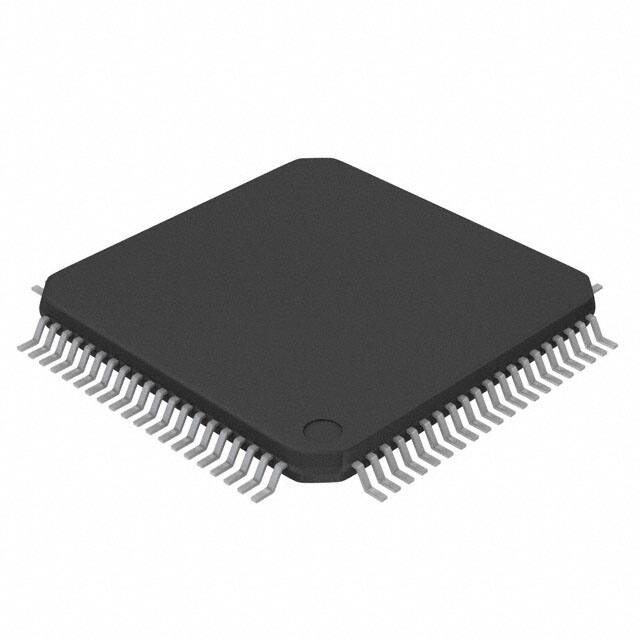


 工商网监
湘ICP备2023018690号
工商网监
湘ICP备2023018690号
