Datasheet
R8C/34W Group, R8C/34X Group, R8C/34Y Group, R8C/34Z Group
RENESAS MCU
1.
R01DS0012EJ0110
Rev.1.10
Jan 31, 2013
Overview
1.1
Features
The R8C/34W Group, R8C/34X Group, R8C/34Y Group, and R8C/34Z Group of single-chip MCUs incorporate
the R8C CPU core, employing sophisticated instructions for a high level of efficiency. With 1 Mbyte of address
space, and it is capable of executing instructions at high speed. In addition, the CPU core boasts a multiplier for
high-speed operation processing.
Power consumption is low, and the supported operating modes allow additional power control. These MCUs are
designed to maximize EMI/EMS performance.
Integration of many peripheral functions, including multifunction timer and serial interface, reduces the number of
system components.
The R8C/34W Group and R8C/34X Group have a single channel CAN module and are suitable for LAN systems in
vehicles and for FA.
The R8C/34Y Group and R8C/34Z Group do not have CAN modules.
The R8C/34W Group and R8C/34Y Group have data flash (1 KB × 4 blocks) with the background operation
(BGO) function.
1.1.1
Applications
Automobiles and others
R01DS0012EJ0110 Rev.1.10
Jan 31, 2013
Page 1 of 67
�R8C/34W Group, R8C/34X Group, R8C/34Y Group, R8C/34Z Group
1.1.2
1. Overview
Specifications
Tables 1.1 and 1.2 outline the Specifications for R8C/34W Group, tables 1.3 and 1.4 outline the Specifications
for R8C/34X Group, tables 1.5 and 1.6 outline the Specifications for R8C/34Y Group, and tables 1.7 and 1.8
outline the Specifications for R8C/34Z Group.
Table 1.1
Item
CPU
Specifications for R8C/34W Group (1)
Function
Central processing
unit
Memory
ROM, RAM, Data
flash
Power Supply Voltage detection
Voltage
circuit
Detection
I/O Ports
Programmable I/O
ports
Clock
Clock generation
circuits
Interrupts
Watchdog Timer
DTC (Data Transfer Controller)
Timer
Timer RA
Timer RB
Timer RC
Timer RD
Timer RE
R01DS0012EJ0110 Rev.1.10
Jan 31, 2013
Specification
R8C CPU core
• Number of fundamental instructions: 89
• Minimum instruction execution time:
50 ns (f(XIN) = 20 MHz, VCC = 2.7 to 5.5 V)
• Multiplier: 16 bits × 16 bits → 32 bits
• Multiply-accumulate instruction: 16 bits × 16 bits + 32 bits → 32 bits
• Operating mode: Single-chip mode (address space: 1 Mbyte)
Refer to Table 1.9 Product List for R8C/34W Group.
• Power-on reset
• Voltage detection 3 (detection level of voltage detection 1 selectable)
• Input-only: 1 pin
• CMOS I/O ports: 43, selectable pull-up resistor
3 circuits: XIN clock oscillation circuit (with on-chip feedback resistor),
High-speed on-chip oscillator (with frequency adjustment function),
Low-speed on-chip oscillator
• Oscillation stop detection: XIN clock oscillation stop detection function
• Frequency divider circuit: Dividing selectable 1, 2, 4, 8, and 16
• Low power consumption modes:
Standard operating mode (high-speed clock, high-speed on-chip oscillator,
low-speed on-chip oscillator), wait mode, stop mode
• Interrupt vectors: 69
• External: 9 sources (INT × 5, key input × 4)
• Priority levels: 7 levels
• 14 bits × 1 (with prescaler)
• Reset start selectable
• Low-speed on-chip oscillator for watchdog timer selectable
• 1 channel
• Activation sources: 31
• Transfer modes: 2 (normal mode, repeat mode)
8 bits (with 8-bit prescaler) × 1
Timer mode (period timer), pulse output mode (output level inverted every
period), event counter mode, pulse width measurement mode, pulse period
measurement mode
8 bits (with 8-bit prescaler) × 1
Timer mode (period timer), programmable waveform generation mode (PWM
output), programmable one-shot generation mode, programmable wait oneshot generation mode
16 bits (with 4 capture/compare registers) × 1
Timer mode (input capture function, output compare function), PWM mode
(output 3 pins), PWM2 mode (PWM output pin)
16 bits (with 4 capture/compare registers) × 2
Timer mode (input capture function, output compare function), PWM mode
(output 6 pins), reset synchronous PWM mode (output three-phase
waveforms (6 pins), sawtooth wave modulation), complementary PWM mode
(output three-phase waveforms (6 pins), triangular wave modulation), PWM3
mode (PWM output 2 pins with fixed period)
8 bits × 1
Output compare mode
Page 2 of 67
�R8C/34W Group, R8C/34X Group, R8C/34Y Group, R8C/34Z Group
Table 1.2
Item
Serial
Interface
1. Overview
Specifications for R8C/34W Group (2)
Function
UART0
UART2
Synchronous Serial
Communication Unit (SSU)
LIN Module
CAN Module
A/D Converter
Flash Memory
Operating Frequency/Supply
Voltage
Current Consumption
Operating Ambient Temperature
Package
Specification
1 channel
Clock synchronous serial I/O, UART
1 channel
Clock synchronous serial I/O, UART, I2C mode (I2C-bus), IE mode (IEBus),
multiprocessor communication function
1 channel
Hardware LIN: 1 (timer RA, UART0)
1 channel, 16 Mailboxes (conforms to the ISO 11898-1)
10-bit resolution × 12 channels, includes sample and hold function, with sweep
mode
• Programming and erasure voltage: VCC = 2.7 to 5.5 V
• Programming and erasure endurance: 10,000 times (data flash)
1,000 times (program ROM)
• Program security: ROM code protect, ID code check
• Debug functions: On-chip debug, on-board flash rewrite function
• Background operation (BGO) function (data flash)
f(XIN) = 20 MHz (VCC = 2.7 to 5.5 V)
Typ. 7 mA (VCC = 5.0 V, f(XIN) = 20 MHz)
-40 to 85°C (J version)
-40 to 125°C (K version) (1)
48-pin LQFP
Package code: PLQP0048KB-A (previous code: 48P6Q-A)
Note:
1. Specify the K version if K version functions are to be used.
R01DS0012EJ0110 Rev.1.10
Jan 31, 2013
Page 3 of 67
�R8C/34W Group, R8C/34X Group, R8C/34Y Group, R8C/34Z Group
Table 1.3
Item
CPU
Specifications for R8C/34X Group (1)
Function
Central processing
unit
Memory
ROM, RAM, Data
flash
Power Supply Voltage detection
Voltage
circuit
Detection
I/O Ports
Programmable I/O
ports
Clock
Clock generation
circuits
Interrupts
Watchdog Timer
DTC (Data Transfer Controller)
Timer
1. Overview
Timer RA
Timer RB
Timer RC
Timer RD
Timer RE
R01DS0012EJ0110 Rev.1.10
Jan 31, 2013
Specification
R8C CPU core
• Number of fundamental instructions: 89
• Minimum instruction execution time:
50 ns (f(XIN) = 20 MHz, VCC = 2.7 to 5.5 V)
• Multiplier: 16 bits × 16 bits → 32 bits
• Multiply-accumulate instruction: 16 bits × 16 bits + 32 bits → 32 bits
• Operating mode: Single-chip mode (address space: 1 Mbyte)
Refer to Table 1.10 Product List for R8C/34X Group.
• Power-on reset
• Voltage detection 3 (detection level of voltage detection 1 selectable)
• Input-only: 1 pin
• CMOS I/O ports: 43, selectable pull-up resistor
3 circuits: XIN clock oscillation circuit (with on-chip feedback resistor),
High-speed on-chip oscillator (with frequency adjustment function),
Low-speed on-chip oscillator
• Oscillation stop detection: XIN clock oscillation stop detection function
• Frequency divider circuit: Dividing selectable 1, 2, 4, 8, and 16
• Low power consumption modes:
Standard operating mode (high-speed clock, high-speed on-chip oscillator,
low-speed on-chip oscillator), wait mode, stop mode
• Interrupt vectors: 69
• External: 9 sources (INT × 5, key input × 4)
• Priority levels: 7 levels
• 14 bits × 1 (with prescaler)
• Reset start selectable
• Low-speed on-chip oscillator for watchdog timer selectable
• 1 channel
• Activation sources: 31
• Transfer modes: 2 (normal mode, repeat mode)
8 bits (with 8-bit prescaler) × 1
Timer mode (period timer), pulse output mode (output level inverted every
period), event counter mode, pulse width measurement mode, pulse period
measurement mode
8 bits (with 8-bit prescaler) × 1
Timer mode (period timer), programmable waveform generation mode (PWM
output), programmable one-shot generation mode, programmable wait oneshot generation mode
16 bits (with 4 capture/compare registers) × 1
Timer mode (input capture function, output compare function), PWM mode
(output 3 pins), PWM2 mode (PWM output pin)
16 bits (with 4 capture/compare registers) × 2
Timer mode (input capture function, output compare function), PWM mode
(output 6 pins), reset synchronous PWM mode (output three-phase
waveforms (6 pins), sawtooth wave modulation), complementary PWM mode
(output three-phase waveforms (6 pins), triangular wave modulation), PWM3
mode (PWM output 2 pins with fixed period)
8 bits × 1
Output compare mode
Page 4 of 67
�R8C/34W Group, R8C/34X Group, R8C/34Y Group, R8C/34Z Group
Table 1.4
Item
Serial
Interface
1. Overview
Specifications for R8C/34X Group (2)
Function
UART0
UART2
Synchronous Serial
Communication Unit (SSU)
LIN Module
CAN Module
A/D Converter
Flash Memory
Operating Frequency/Supply
Voltage
Current Consumption
Operating Ambient Temperature
Package
Specification
1 channel
Clock synchronous serial I/O, UART
1 channel
Clock synchronous serial I/O, UART, I2C mode (I2C-bus), IE mode (IEBus),
multiprocessor communication function
1 channel
Hardware LIN: 1 (timer RA, UART0)
1 channel, 16 Mailboxes (conforms to the ISO 11898-1)
10-bit resolution × 12 channels, includes sample and hold function, with sweep
mode
• Programming and erasure voltage: VCC = 2.7 to 5.5 V
• Programming and erasure endurance: 100 times (program ROM)
• Program security: ROM code protect, ID code check
• Debug functions: On-chip debug, on-board flash rewrite function
f(XIN) = 20 MHz (VCC = 2.7 to 5.5 V)
Typ. 7 mA (VCC = 5.0 V, f(XIN) = 20 MHz)
-40 to 85°C (J version)
-40 to 125°C (K version) (1)
48-pin LQFP
Package code: PLQP0048KB-A (previous code: 48P6Q-A)
Note:
1. Specify the K version if K version functions are to be used.
R01DS0012EJ0110 Rev.1.10
Jan 31, 2013
Page 5 of 67
�R8C/34W Group, R8C/34X Group, R8C/34Y Group, R8C/34Z Group
Table 1.5
Item
CPU
Specifications for R8C/34Y Group (1)
Function
Central processing
unit
Memory
ROM, RAM, Data
flash
Power Supply Voltage detection
Voltage
circuit
Detection
I/O Ports
Programmable I/O
ports
Clock
Clock generation
circuits
Interrupts
Watchdog Timer
DTC (Data Transfer Controller)
Timer
1. Overview
Timer RA
Timer RB
Timer RC
Timer RD
Timer RE
R01DS0012EJ0110 Rev.1.10
Jan 31, 2013
Specification
R8C CPU core
• Number of fundamental instructions: 89
• Minimum instruction execution time:
50 ns (f(XIN) = 20 MHz, VCC = 2.7 to 5.5 V)
• Multiplier: 16 bits × 16 bits → 32 bits
• Multiply-accumulate instruction: 16 bits × 16 bits + 32 bits → 32 bits
• Operating mode: Single-chip mode (address space: 1 Mbyte)
Refer to Table 1.11 Product List for R8C/34Y Group.
• Power-on reset
• Voltage detection 3 (detection level of voltage detection 1 selectable)
• Input-only: 1 pin
• CMOS I/O ports: 43, selectable pull-up resistor
3 circuits: XIN clock oscillation circuit (with on-chip feedback resistor),
High-speed on-chip oscillator (with frequency adjustment function),
Low-speed on-chip oscillator
• Oscillation stop detection: XIN clock oscillation stop detection function
• Frequency divider circuit: Dividing selectable 1, 2, 4, 8, and 16
• Low power consumption modes:
Standard operating mode (high-speed clock, high-speed on-chip oscillator,
low-speed on-chip oscillator), wait mode, stop mode
• Interrupt vectors: 69
• External: 9 sources (INT × 5, key input × 4)
• Priority levels: 7 levels
• 14 bits × 1 (with prescaler)
• Reset start selectable
• Low-speed on-chip oscillator for watchdog timer selectable
• 1 channel
• Activation sources: 31
• Transfer modes: 2 (normal mode, repeat mode)
8 bits (with 8-bit prescaler) × 1
Timer mode (period timer), pulse output mode (output level inverted every
period), event counter mode, pulse width measurement mode, pulse period
measurement mode
8 bits (with 8-bit prescaler) × 1
Timer mode (period timer), programmable waveform generation mode (PWM
output), programmable one-shot generation mode, programmable wait oneshot generation mode
16 bits (with 4 capture/compare registers) × 1
Timer mode (input capture function, output compare function), PWM mode
(output 3 pins), PWM2 mode (PWM output pin)
16 bits (with 4 capture/compare registers) × 2
Timer mode (input capture function, output compare function), PWM mode
(output 6 pins), reset synchronous PWM mode (output three-phase
waveforms (6 pins), sawtooth wave modulation), complementary PWM mode
(output three-phase waveforms (6 pins), triangular wave modulation), PWM3
mode (PWM output 2 pins with fixed period)
8 bits × 1
Output compare mode
Page 6 of 67
�R8C/34W Group, R8C/34X Group, R8C/34Y Group, R8C/34Z Group
Table 1.6
Item
Serial
Interface
1. Overview
Specifications for R8C/34Y Group (2)
Function
UART0
UART2
Synchronous Serial
Communication Unit (SSU)
LIN Module
A/D Converter
Flash Memory
Operating Frequency/Supply
Voltage
Current Consumption
Operating Ambient Temperature
Package
Specification
1 channel
Clock synchronous serial I/O, UART
1 channel
Clock synchronous serial I/O, UART, I2C mode (I2C-bus), IE mode (IEBus),
multiprocessor communication function
1 channel
Hardware LIN: 1 (timer RA, UART0)
10-bit resolution × 12 channels, includes sample and hold function, with sweep
mode
• Programming and erasure voltage: VCC = 2.7 to 5.5 V
• Programming and erasure endurance: 10,000 times (data flash)
1,000 times (program ROM)
• Program security: ROM code protect, ID code check
• Debug functions: On-chip debug, on-board flash rewrite function
• Background operation (BGO) function (data flash)
f(XIN) = 20 MHz (VCC = 2.7 to 5.5 V)
Typ. 7 mA (VCC = 5.0 V, f(XIN) = 20 MHz)
-40 to 85°C (J version)
-40 to 125°C (K version) (1)
48-pin LQFP
Package code: PLQP0048KB-A (previous code: 48P6Q-A)
Note:
1. Specify the K version if K version functions are to be used.
R01DS0012EJ0110 Rev.1.10
Jan 31, 2013
Page 7 of 67
�R8C/34W Group, R8C/34X Group, R8C/34Y Group, R8C/34Z Group
Table 1.7
Item
CPU
Specifications for R8C/34Z Group (1)
Function
Central processing
unit
Memory
ROM, RAM, Data
flash
Power Supply Voltage detection
Voltage
circuit
Detection
I/O Ports
Programmable I/O
ports
Clock
Clock generation
circuits
Interrupts
Watchdog Timer
DTC (Data Transfer Controller)
Timer
1. Overview
Timer RA
Timer RB
Timer RC
Timer RD
Timer RE
R01DS0012EJ0110 Rev.1.10
Jan 31, 2013
Specification
R8C CPU core
• Number of fundamental instructions: 89
• Minimum instruction execution time:
50 ns (f(XIN) = 20 MHz, VCC = 2.7 to 5.5 V)
• Multiplier: 16 bits × 16 bits → 32 bits
• Multiply-accumulate instruction: 16 bits × 16 bits + 32 bits → 32 bits
• Operating mode: Single-chip mode (address space: 1 Mbyte)
Refer to Table 1.12 Product List for R8C/34Z Group.
• Power-on reset
• Voltage detection 3 (detection level of voltage detection 1 selectable)
• Input-only: 1 pin
• CMOS I/O ports: 43, selectable pull-up resistor
3 circuits: XIN clock oscillation circuit (with on-chip feedback resistor),
High-speed on-chip oscillator (with frequency adjustment function),
Low-speed on-chip oscillator
• Oscillation stop detection: XIN clock oscillation stop detection function
• Frequency divider circuit: Dividing selectable 1, 2, 4, 8, and 16
• Low power consumption modes:
Standard operating mode (high-speed clock, high-speed on-chip oscillator,
low-speed on-chip oscillator), wait mode, stop mode
• Interrupt vectors: 69
• External: 9 sources (INT × 5, key input × 4)
• Priority levels: 7 levels
• 14 bits × 1 (with prescaler)
• Reset start selectable
• Low-speed on-chip oscillator for watchdog timer selectable
• 1 channel
• Activation sources: 31
• Transfer modes: 2 (normal mode, repeat mode)
8 bits (with 8-bit prescaler) × 1
Timer mode (period timer), pulse output mode (output level inverted every
period), event counter mode, pulse width measurement mode, pulse period
measurement mode
8 bits (with 8-bit prescaler) × 1
Timer mode (period timer), programmable waveform generation mode (PWM
output), programmable one-shot generation mode, programmable wait oneshot generation mode
16 bits (with 4 capture/compare registers) × 1
Timer mode (input capture function, output compare function), PWM mode
(output 3 pins), PWM2 mode (PWM output pin)
16 bits (with 4 capture/compare registers) × 2
Timer mode (input capture function, output compare function), PWM mode
(output 6 pins), reset synchronous PWM mode (output three-phase
waveforms (6 pins), sawtooth wave modulation), complementary PWM mode
(output three-phase waveforms (6 pins), triangular wave modulation), PWM3
mode (PWM output 2 pins with fixed period)
8 bits × 1
Output compare mode
Page 8 of 67
�R8C/34W Group, R8C/34X Group, R8C/34Y Group, R8C/34Z Group
Table 1.8
Item
Serial
Interface
1. Overview
Specifications for R8C/34Z Group (2)
Function
UART0
UART2
Synchronous Serial
Communication Unit (SSU)
LIN Module
A/D Converter
Flash Memory
Operating Frequency/Supply
Voltage
Current Consumption
Operating Ambient Temperature
Package
Specification
1 channel
Clock synchronous serial I/O, UART
1 channel
Clock synchronous serial I/O, UART, I2C mode (I2C-bus), IE mode (IEBus),
multiprocessor communication function
1 channel
Hardware LIN: 1 (timer RA, UART0)
10-bit resolution × 12 channels, includes sample and hold function, with sweep
mode
• Programming and erasure voltage: VCC = 2.7 to 5.5 V
• Programming and erasure endurance: 100 times (program ROM)
• Program security: ROM code protect, ID code check
• Debug functions: On-chip debug, on-board flash rewrite function
f(XIN) = 20 MHz (VCC = 2.7 to 5.5 V)
Typ. 7 mA (VCC = 5.0 V, f(XIN) = 20 MHz)
-40 to 85°C (J version)
-40 to 125°C (K version) (1)
48-pin LQFP
Package code: PLQP0048KB-A (previous code: 48P6Q-A)
Note:
1. Specify the K version if K version functions are to be used.
R01DS0012EJ0110 Rev.1.10
Jan 31, 2013
Page 9 of 67
�R8C/34W Group, R8C/34X Group, R8C/34Y Group, R8C/34Z Group
1.2
1. Overview
Product List
Table 1.9 lists Product List for R8C/34W Group, Table 1.10 lists Product List for R8C/34X Group, Table 1.11 lists
Product List for R8C/34Y Group, and Table 1.12 lists Product List for R8C/34Z Group.
Table 1.9
Product List for R8C/34W Group
Part No.
R5F21346WJFP
R5F21347WJFP
R5F21348WJFP
R5F2134AWJFP
R5F2134CWJFP
R5F21346WKFP
R5F21347WKFP
R5F21348WKFP
R5F2134AWKFP
R5F2134CWKFP
Part No.
ROM Capacity
Program ROM
Data flash
32 Kbytes
1 Kbyte × 4
48 Kbytes
1 Kbyte × 4
64 Kbytes
1 Kbyte × 4
96 Kbytes
1 Kbyte × 4
128 Kbytes
1 Kbyte × 4
32 Kbytes
1 Kbyte × 4
48 Kbytes
1 Kbyte × 4
64 Kbytes
1 Kbyte × 4
96 Kbytes
1 Kbyte × 4
128 Kbytes
1 Kbyte × 4
Current of Jan 2013
RAM
Capacity
2.5 Kbytes
4 Kbytes
6 Kbytes
8 Kbytes
10 Kbytes
2.5 Kbytes
4 Kbytes
6 Kbytes
8 Kbytes
10 Kbytes
Package Type
PLQP0048KB-A
PLQP0048KB-A
PLQP0048KB-A
PLQP0048KB-A
PLQP0048KB-A
PLQP0048KB-A
PLQP0048KB-A
PLQP0048KB-A
PLQP0048KB-A
PLQP0048KB-A
Remarks
J version
K version
R 5 F 21 34 6 W J FP
Package type:
FP: PLQP0048KB-A (0.5 mm pin-pitch, 7 mm square body)
CAN, Data Flash
W: CAN module and Data Flash
X : CAN module but no Data Flash
Y : Data Flash but no CAN module
Z : None
Classification
J: Operating ambient temperature −40 °C to 85 °C
K: Operating ambient temperature −40 °C to 125 °C
ROM capacity
6: 32 KB
7: 48 KB
8: 64 KB
A: 96 KB
C: 128 KB
R8C/34W Group
R8C/3x Series
Memory type
F: Flash memory
Renesas MCU
Renesas semiconductor
Figure 1.1
Part Number, Memory Size, and Package of R8C/34W Group
R01DS0012EJ0110 Rev.1.10
Jan 31, 2013
Page 10 of 67
�R8C/34W Group, R8C/34X Group, R8C/34Y Group, R8C/34Z Group
1. Overview
Table 1.10
Product List for R8C/34X Group
ROM Capacity
Part No.
RAM Capacity
Program ROM
R5F21346XJFP
32 Kbytes
2.5 Kbytes
R5F21347XJFP
48 Kbytes
4 Kbytes
R5F21348XJFP
64 Kbytes
6 Kbytes
R5F2134AXJFP
96 Kbytes
8 Kbytes
R5F2134CXJFP
128 Kbytes
10 Kbytes
R5F21346XKFP
32 Kbytes
2.5 Kbytes
R5F21347XKFP
48 Kbytes
4 Kbytes
R5F21348XKFP
64 Kbytes
6 Kbytes
R5F2134AXKFP
96 Kbytes
8 Kbytes
R5F2134CXKFP
128 Kbytes
10 Kbytes
Part No.
Current of Jan 2013
Package Type
PLQP0048KB-A
PLQP0048KB-A
PLQP0048KB-A
PLQP0048KB-A
PLQP0048KB-A
PLQP0048KB-A
PLQP0048KB-A
PLQP0048KB-A
PLQP0048KB-A
PLQP0048KB-A
Remarks
J version
K version
R 5 F 21 34 6 X J FP
Package type:
FP: PLQP0048KB-A (0.5 mm pin-pitch, 7 mm square body)
CAN, Data Flash
W: CAN module and Data Flash
X : CAN module but no Data Flash
Y : Data Flash but no CAN module
Z : None
Classification
J: Operating ambient temperature −40 °C to 85 °C
K: Operating ambient temperature −40 °C to 125 °C
ROM capacity
6: 32 KB
7: 48 KB
8: 64 KB
A: 96 KB
C: 128 KB
R8C/34X Group
R8C/3x Series
Memory type
F: Flash memory
Renesas MCU
Renesas semiconductor
Figure 1.2
Part Number, Memory Size, and Package of R8C/34X Group
R01DS0012EJ0110 Rev.1.10
Jan 31, 2013
Page 11 of 67
�R8C/34W Group, R8C/34X Group, R8C/34Y Group, R8C/34Z Group
Product List for R8C/34Y Group
ROM Capacity
Part No.
Program ROM
Data flash
R5F21346YJFP
32 Kbytes
1 Kbyte × 4
R5F21347YJFP
48 Kbytes
1 Kbyte × 4
R5F21348YJFP
64 Kbytes
1 Kbyte × 4
R5F2134AYJFP
96 Kbytes
1 Kbyte × 4
R5F2134CYJFP
128 Kbytes
1 Kbyte × 4
R5F21346YKFP
32 Kbytes
1 Kbyte × 4
R5F21347YKFP
48 Kbytes
1 Kbyte × 4
R5F21348YKFP
64 Kbytes
1 Kbyte × 4
R5F2134AYKFP
96 Kbytes
1 Kbyte × 4
R5F2134CYKFP
128 Kbytes
1 Kbyte × 4
1. Overview
Table 1.11
Part No.
Current of Jan 2013
RAM
Capacity
2.5 Kbytes
4 Kbytes
6 Kbytes
8 Kbytes
10 Kbytes
2.5 Kbytes
4 Kbytes
6 Kbytes
8 Kbytes
10 Kbytes
Package Type
PLQP0048KB-A
PLQP0048KB-A
PLQP0048KB-A
PLQP0048KB-A
PLQP0048KB-A
PLQP0048KB-A
PLQP0048KB-A
PLQP0048KB-A
PLQP0048KB-A
PLQP0048KB-A
Remarks
J version
K version
R 5 F 21 34 6 Y J FP
Package type:
FP: PLQP0048KB-A (0.5 mm pin-pitch, 7 mm square body)
CAN, Data Flash
W: CAN module and Data Flash
X : CAN module but no Data Flash
Y : Data Flash but no CAN module
Z : None
Classification
J: Operating ambient temperature −40 °C to 85 °C
K: Operating ambient temperature −40 °C to 125 °C
ROM capacity
6: 32 KB
7: 48 KB
8: 64 KB
A: 96 KB
C: 128 KB
R8C/34Y Group
R8C/3x Series
Memory type
F: Flash memory
Renesas MCU
Renesas semiconductor
Figure 1.3
Part Number, Memory Size, and Package of R8C/34Y Group
R01DS0012EJ0110 Rev.1.10
Jan 31, 2013
Page 12 of 67
�R8C/34W Group, R8C/34X Group, R8C/34Y Group, R8C/34Z Group
1. Overview
Table 1.12
Product List for R8C/34Z Group
ROM Capacity
Part No.
RAM Capacity
Program ROM
R5F21346ZJFP
32 Kbytes
2.5 Kbytes
R5F21347ZJFP
48 Kbytes
4 Kbytes
R5F21348ZJFP
64 Kbytes
6 Kbytes
R5F2134AZJFP
96 Kbytes
8 Kbytes
R5F2134CZJFP
128 Kbytes
10 Kbytes
R5F21346ZKFP
32 Kbytes
2.5 Kbytes
R5F21347ZKFP
48 Kbytes
4 Kbytes
R5F21348ZKFP
64 Kbytes
6 Kbytes
R5F2134AZKFP
96 Kbytes
8 Kbytes
R5F2134CZKFP
128 Kbytes
10 Kbytes
Part No.
Current of Jan 2013
Package Type
PLQP0048KB-A
PLQP0048KB-A
PLQP0048KB-A
PLQP0048KB-A
PLQP0048KB-A
PLQP0048KB-A
PLQP0048KB-A
PLQP0048KB-A
PLQP0048KB-A
PLQP0048KB-A
Remarks
J version
K version
R 5 F 21 34 6 Z J FP
Package type:
FP: PLQP0048KB-A (0.5 mm pin-pitch, 7 mm square body)
CAN, Data Flash
W: CAN module and Data Flash
X : CAN module but no Data Flash
Y : Data Flash but no CAN module
Z : None
Classification
J: Operating ambient temperature −40 °C to 85 °C
K: Operating ambient temperature −40 °C to 125 °C
ROM capacity
6: 32 KB
7: 48 KB
8: 64 KB
A: 96 KB
C: 128 KB
R8C/34Z Group
R8C/3x Series
Memory type
F: Flash memory
Renesas MCU
Renesas semiconductor
Figure 1.4
Part Number, Memory Size, and Package of R8C/34Z Group
R01DS0012EJ0110 Rev.1.10
Jan 31, 2013
Page 13 of 67
�R8C/34W Group, R8C/34X Group, R8C/34Y Group, R8C/34Z Group
1.3
1. Overview
Block Diagram
Figure 1.5 shows a Block Diagram.
I/O ports
8
8
8
6
Port P0
Port P1
Port P2
Port P3
5
1
8
Port P4
Port 6
Peripheral functions
Timers
Timer RA (8 bits)
Timer RB (8 bits)
Timer RC (16 bits)
Timer RD (16 bits × 2)
Timer RE (8 bits)
System clock
generation circuit
A/D converter
(10 bits × 12 channels)
XIN-XOUT
High-speed on-chip oscillator
Low-speed on-chip oscillator
UART or
clock synchronous serial I/O
(8 bits × 2 channels)
CAN module (3)
(1 channel)
DTC
SSU
(8 bits × 1 channel)
LIN module
(1 channel)
Voltage detection circuit
Memory
R8C CPU core
Watchdog timer
(14 bits)
R0H
R1H
R0L
R1L
R2
R3
A0
A1
FB
SB
USP
ISP
INTB
PC
ROM (1)
RAM (2)
FLG
Multiplier
Notes:
1. ROM size varies with MCU type.
2. RAM size varies with MCU type.
3. Only in the R8C/34W Group and R8C/34X Group.
Figure 1.5
Block Diagram
R01DS0012EJ0110 Rev.1.10
Jan 31, 2013
Page 14 of 67
�R8C/34W Group, R8C/34X Group, R8C/34Y Group, R8C/34Z Group
1.4
1. Overview
Pin Assignment
P0_7/AN0
P6_3
P6_4
P6_5/INT4/(CLK2)(1)
P3_0/(TRAO)(1)
P3_1/(TRBO)(1)
P1_0/KI0/AN8
P1_1/KI1/TRCIOA/TRCTRG/AN9
P1_2/KI2/TRCIOB/AN10
P6_7/(INT3)(1)/TRCIOD/(RXD2)/(SCL2)(1)
P6_6/INT2/TRCIOC/(TXD2)/(SDA2)(1)
P4_5/INT0/ADTRG
Figure 1.6 shows Pin Assignment (Top View). Tables 1.13 and 1.14 outline the Pin Name Information by Pin
Number.
36
P0_6/AN1
P0_5/AN2
P0_4/TREO/AN3
VREF/P4_2(3)
P6_0/(TREO)(1)
P6_2/CRX0(2)
P6_1/CTX0(2)
P0_3/AN4
P0_2/AN5
P0_1/AN6
P0_0/AN7
P3_7/(TRAO)(1)/(TXD2)/(SDA2)/(RXD2)/(SCL2)(1)/SSO
35
34
33
32
31
30
29
28
27
26
25
37
24
38
23
39
R8C/34W Group
R8C/34X Group
R8C/34Y Group
R8C/34Z Group
22
PLQP0048KB-A (48P6Q-A)
18
40
41
42
43
21
20
19
44
17
(Top view)
45
16
46
15
47
14
13
48
2
3
4
5
6
7
8
9
10 11 12
P3_5/(CLK2)(1)/SSCK
P3_3/INT3/CTS2/RTS2/(SSI)(1)/SCS
P3_4/(TXD2)/(SDA2)/(RXD2)/(SCL2)(1)/SSI/(SCS)(1)
MODE
P4_3
P4_4
RESET
XOUT/P4_7
VSS/AVSS
XIN/P4_6
VCC/AVCC
P2_7/TRDIOD1
1
P1_3/KI3/TRBO/AN11
P1_4/TRCCLK/TXD0
P1_5/(INT1)(1)/(TRAIO)(1)/RXD0
P1_6/CLK0
P1_7/INT1/(TRAIO)(1)
P2_0/TRDIOA0/TRDCLK
P2_1/TRDIOB0
P2_2/TRDIOC0
P2_3/TRDIOD0
P2_4/TRDIOA1
P2_5/TRDIOB1
P2_6/TRDIOC1
Notes:
1. Can be assigned to the pin in parentheses by a program.
2. Only in the R8C/34W Group and R8C/34X Group.
3. P4_2 is an input-only pin.
4. Confirm the pin 1 position on the package by referring to the Package Dimensions.
Figure 1.6
Pin Assignment (Top View)
R01DS0012EJ0110 Rev.1.10
Jan 31, 2013
Page 15 of 67
�R8C/34W Group, R8C/34X Group, R8C/34Y Group, R8C/34Z Group
Table 1.13
1. Overview
Pin Name Information by Pin Number (1)
I/O Pin Functions for Peripheral Modules
Pin
Number
Control Pin
Port
1
P3_5
2
P3_3
3
P3_4
Interrupt
Timer
INT3
Serial Interface
SSU
(CLK2) (1)
SSCK
CTS2/RTS2
(SSI) (1)/SCS
(TXD2)/(SDA2)/
(RXD2)/(SCL2)
SSI/(SCS) (1)
CAN
Module (2)
A/D Converter
Voltage Detection
Circuit
(1)
4
MODE
5
P4_3
6
P4_4
7
RESET
8
XOUT
9
VSS/AVSS
10
XIN
11
VCC/AVCC
P4_7
P4_6
12
P2_7
TRDIOD1
13
P2_6
TRDIOC1
14
P2_5
TRDIOB1
15
P2_4
TRDIOA1
16
P2_3
TRDIOD0
17
P2_2
TRDIOC0
18
P2_1
TRDIOB0
19
P2_0
TRDIOA0/
TRDCLK
20
P1_7
21
P1_6
22
P1_5
23
P1_4
24
P1_3
KI3
25
P4_5
INT0
26
P6_6
INT2
INT1
(TRAIO)
(1)
CLK0
INT1 (1)
(TRAIO)
(1)
TRCCLK
RXD0
TXD0
TRBO
AN11
ADTRG
TRCIOC
(TXD2)/(SDA2)
(1)
Notes:
1. This can be assigned to the pin in parentheses by a program.
2. Only for the R8C/34W Group and R8C/34X Group.
R01DS0012EJ0110 Rev.1.10
Jan 31, 2013
Page 16 of 67
�R8C/34W Group, R8C/34X Group, R8C/34Y Group, R8C/34Z Group
Table 1.14
1. Overview
Pin Name Information by Pin Number (2)
I/O Pin Functions for Peripheral Modules
Pin
Number
Control Pin
Port
Interrupt
Timer
Serial Interface
SSU
CAN
Module (2)
A/D Converter
Voltage Detection
Circuit
(RXD2)/(SCL2)
27
P6_7
INT3 (1)
TRCIOD
28
P1_2
KI2
TRCIOB
AN10
29
P1_1
KI1
TRCIOA/
TRCTRG
AN9
30
P1_0
KI0
31
P3_1
(1)
AN8
(TRBO)
(1)
(TRAO)
32
P3_0
33
P6_5
34
P6_4
35
P6_3
36
P0_7
AN0
37
P0_6
AN1
38
P0_5
AN2
39
P0_4
40
P4_2
41
P6_0
42
P6_2
CRX0 (2)
43
P6_1
CTX0 (2)
44
P0_3
AN4
45
P0_2
AN5
46
P0_1
AN6
47
P0_0
AN7
48
P3_7
(1)
(CLK2) (1)
INT4
TREO
AN3
VREF
(TREO)
(1)
(TRAO)
(1)
(TXD2)/(SDA2)/
(RXD2)/(SCL2)
SSO
(1)
Notes:
1. This can be assigned to the pin in parentheses by a program.
2. Only for the R8C/34W Group and R8C/34X Group.
R01DS0012EJ0110 Rev.1.10
Jan 31, 2013
Page 17 of 67
�R8C/34W Group, R8C/34X Group, R8C/34Y Group, R8C/34Z Group
1.5
1. Overview
Pin Functions
Tables 1.15 and 1.16 list Pin Functions.
Table 1.15
Pin Functions (1)
Item
Pin Name
I/O Type
Description
Power supply input VCC, VSS
−
Apply 2.7 V to 5.5 V to the VCC pin. Apply 0 V to the VSS pin.
Analog power
supply input
AVCC, AVSS
−
Power supply for the A/D converter.
Connect a capacitor between AVCC and AVSS.
Reset input
RESET
I
Input “L” on this pin resets the MCU.
MODE
MODE
I
Connect this pin to VCC via a resistor.
XIN clock input
XIN
I
XIN clock output
XOUT
These pins are provided for XIN clock generation circuit I/O.
Connect a ceramic resonator or a crystal oscillator between
the XIN and XOUT pins (1). To use an external clock, input it
to the XOUT pin and leave the XIN pin open.
INT interrupt input
I/O
INT0 to INT4
I
INT interrupt input pins.
Key input interrupt
KI0 to KI3
I
Key input interrupt input pins
Timer RA
TRAIO
I/O
Timer RA I/O pin
TRAO
O
Timer RA output pin
TRBO
O
Timer RB output pin
TRCCLK
I
External clock input pin
TRCTRG
I
External trigger input pin
Timer RB
Timer RC
Timer RD
Timer RE
Serial interface
SSU
TRCIOA, TRCIOB,
TRCIOC, TRCIOD
I/O
Timer RC I/O pins
TRDIOA0, TRDIOA1,
TRDIOB0, TRDIOB1,
TRDIOC0, TRDIOC1,
TRDIOD0, TRDIOD1
I/O
Timer RD I/O pins
TRDCLK
I
External clock input pin
TREO
O
Divided clock output pin
CLK0, CLK2
I/O
RXD0, RXD2
I
Serial data input pins
Transfer clock I/O pins
TXD0, TXD2
O
Serial data output pins
CTS2
I
Transmission control input pin
RTS2
O
Reception control output pin
SCL2
I/O
I2C mode clock I/O pin
SDA2
I/O
I2C mode data I/O pin
SSI
I/O
Data I/O pin
SCS
I/O
Chip-select signal I/O pin
SSCK
I/O
Clock I/O pin
SSO
I/O
Data I/O pin
I: Input
O: Output
I/O: Input and output
Note:
1. Refer to the oscillator manufacturer for oscillation characteristics.
R01DS0012EJ0110 Rev.1.10
Jan 31, 2013
Page 18 of 67
�R8C/34W Group, R8C/34X Group, R8C/34Y Group, R8C/34Z Group
Table 1.16
1. Overview
Pin Functions (2)
Item
Pin Name
CAN module
I/O Type
Description
CRX0
(1)
I
CAN data input pin
CTX0
(1)
O
CAN data output pin
Reference voltage
input
VREF
I
Reference voltage input pin to A/D converter
A/D converter
AN0 to AN11
I
Analog input pins to A/D converter
ADTRG
I
AD external trigger input pin
I/O port
P0_0 to P0_7,
P1_0 to P1_7,
P2_0 to P2_7,
P3_0 to P3_1,
P3_3 to P3_5, P3_7,
P4_3 to P4_7,
P6_0 to P6_7
Input port
P4_2
I: Input
Note:
O: Output
I/O
I
CMOS I/O ports. Each port has an I/O select direction
register, allowing each pin in the port to be directed for input
or output individually.
Any port set to input can be set to use a pull-up resistor or not
by a program.
Input-only port
I/O: Input and output
1. Only in the R8C/34W Group and R8C/34X Group.
R01DS0012EJ0110 Rev.1.10
Jan 31, 2013
Page 19 of 67
�R8C/34W Group, R8C/34X Group, R8C/34Y Group, R8C/34Z Group
2.
2. Central Processing Unit (CPU)
Central Processing Unit (CPU)
Figure 2.1 shows the CPU Registers. The CPU contains 13 registers. R0, R1, R2, R3, A0, A1, and FB configure a
register bank. There are two sets of register bank.
b31
b15
R2
R3
b8b7
b0
R0H (high-order of R0) R0L (low-order of R0)
R1H (high-order of R1) R1L (low-order of R1)
Data registers (1)
R2
R3
A0
A1
FB
b19
b15
Address registers (1)
Frame base register (1)
b0
Interrupt table register
INTBL
INTBH
The 4 high order bits of INTB are INTBH and
the 16 low order bits of INTB are INTBL.
b19
b0
Program counter
PC
b15
b0
USP
User stack pointer
ISP
Interrupt stack pointer
SB
Static base register
b15
b0
FLG
b15
b8
IPL
b7
Flag register
b0
U I O B S Z D C
Carry flag
Debug flag
Zero flag
Sign flag
Register bank select flag
Overflow flag
Interrupt enable flag
Stack pointer select flag
Reserved bit
Processor interrupt priority level
Reserved bit
Note:
1. These registers comprise a register bank. There are two register banks.
Figure 2.1
CPU Registers
R01DS0012EJ0110 Rev.1.10
Jan 31, 2013
Page 20 of 67
�R8C/34W Group, R8C/34X Group, R8C/34Y Group, R8C/34Z Group
2.1
2. Central Processing Unit (CPU)
Data Registers (R0, R1, R2, and R3)
R0 is a 16-bit register for transfer, arithmetic, and logic operations. The same applies to R1 to R3. R0 can be split
into high-order bits (R0H) and low-order bits (R0L) to be used separately as 8-bit data registers. R1H and R1L are
analogous to R0H and R0L. R2 can be combined with R0 and used as a 32-bit data register (R2R0). R3R1 is
analogous to R2R0.
2.2
Address Registers (A0 and A1)
A0 is a 16-bit register for address register indirect addressing and address register relative addressing. It is also
used for transfer, arithmetic, and logic operations. A1 is analogous to A0. A1 can be combined with A0 and as a 32bit address register (A1A0).
2.3
Frame Base Register (FB)
FB is a 16-bit register for FB relative addressing.
2.4
Interrupt Table Register (INTB)
INTB is a 20-bit register that indicates the start address of an interrupt vector table.
2.5
Program Counter (PC)
PC is 20 bits wide and indicates the address of the next instruction to be executed.
2.6
User Stack Pointer (USP) and Interrupt Stack Pointer (ISP)
The stack pointers (SP), USP, and ISP, are each 16 bits wide. The U flag of FLG is used to switch between
USP and ISP.
2.7
Static Base Register (SB)
SB is a 16-bit register for SB relative addressing.
2.8
Flag Register (FLG)
FLG is an 11-bit register indicating the CPU state.
2.8.1
Carry Flag (C)
The C flag retains carry, borrow, or shift-out bits that have been generated by the arithmetic and logic unit.
2.8.2
Debug Flag (D)
The D flag is for debugging only. Set it to 0.
2.8.3
Zero Flag (Z)
The Z flag is set to 1 when an arithmetic operation results in 0; otherwise to 0.
2.8.4
Sign Flag (S)
The S flag is set to 1 when an arithmetic operation results in a negative value; otherwise to 0.
2.8.5
Register Bank Select Flag (B)
Register bank 0 is selected when the B flag is 0. Register bank 1 is selected when this flag is set to 1.
2.8.6
Overflow Flag (O)
The O flag is set to 1 when an operation results in an overflow; otherwise to 0.
R01DS0012EJ0110 Rev.1.10
Jan 31, 2013
Page 21 of 67
�R8C/34W Group, R8C/34X Group, R8C/34Y Group, R8C/34Z Group
2.8.7
2. Central Processing Unit (CPU)
Interrupt Enable Flag (I)
The I flag enables maskable interrupts.
Interrupt are disabled when the I flag is set to 0, and are enabled when the I flag is set to 1. The I flag is set to 0
when an interrupt request is acknowledged.
2.8.8
Stack Pointer Select Flag (U)
ISP is selected when the U flag is set to 0; USP is selected when the U flag is set to 1.
The U flag is set to 0 when a hardware interrupt request is acknowledged or the INT instruction of software
interrupt numbers 0 to 31 is executed.
2.8.9
Processor Interrupt Priority Level (IPL)
IPL is 3 bits wide and assigns processor interrupt priority levels from level 0 to level 7.
If a requested interrupt has higher priority than IPL, the interrupt is enabled.
2.8.10
Reserved Bit
If necessary, set to 0. When read, the content is undefined.
R01DS0012EJ0110 Rev.1.10
Jan 31, 2013
Page 22 of 67
�R8C/34W Group, R8C/34X Group, R8C/34Y Group, R8C/34Z Group
3.
3. Memory
Memory
3.1
R8C/34W Group
Figure 3.1 is a Memory Map of R8C/34W Group. The R8C/34W Group has a 1-Mbyte address space from
addresses 00000h to FFFFFh. The internal ROM (program ROM) is allocated lower addresses, beginning with
address 0FFFFh. For example, a 48-Kbyte internal ROM area is allocated addresses 04000h to 0FFFFh.
The fixed interrupt vector table is allocated addresses 0FFDCh to 0FFFFh. The starting address of each interrupt
routine is stored here.
The internal ROM (data flash) is allocated addresses 03000h to 03FFFh.
The internal RAM is allocated higher addresses, beginning with address 00400h. For example, a 4-Kbyte internal
RAM area is allocated addresses 00400h to 013FFh. The internal RAM is used not only for data storage but also as
a stack area when a subroutine is called or when an interrupt request is acknowledged.
Special function registers (SFRs) are allocated addresses 00000h to 002FFh and 02C00h to 02FFFh (the SFR areas
for the CAN, DTC, and other modules). Peripheral function control registers are allocated here. All unallocated
spaces within the SFRs are reserved and cannot be accessed by users.
00000h
SFR
002FFh
(Refer to 4. Special
Function Registers
(SFRs))
00400h
Internal RAM
0XXXXh
02C00h
02FFFh
03000h
SFR (2)
0FFDCh
Undefined instruction
Overflow
BRK instruction
Address match
Single step
(Refer to 4. Special Function
Registers (SFRs))
Internal ROM
(data flash) (1)
03FFFh
0YYYYh
Watchdog timer, oscillation stop detection, voltage monitor
Address break
(Reserved)
Reset
Internal ROM
(program ROM)
0FFFFh
0FFFFh
Internal ROM
(program ROM)
ZZZZZh
FFFFFh
Notes:
1. The Data Flash memory indicates blocks A (1 Kbyte), B (1 Kbyte), C (1 Kbyte), and D (1 Kbyte).
2. The SFR areas for the CAN, DTC and other modules are allocated to addresses 02C00h to 02FFFh.
3. The blank areas are reserved and cannot be accessed by users.
Internal ROM
Part Number
Internal RAM
Address ZZZZZh
Size
Address 0YYYYh
Size
Address 0XXXXh
R5F21346WJFP, R5F21346WKFP
32 Kbytes
08000h
2.5 Kbytes
00DFFh
R5F21347WJFP, R5F21347WKFP
R5F21348WJFP, R5F21348WKFP
R5F2134AWJFP, R5F2134AWKFP
R5F2134CWJFP, R5F2134CWKFP
48 Kbytes
64 Kbytes
96 Kbytes
04000h
04000h
04000h
13FFFh
1BFFFh
4 Kbytes
6 Kbytes
8 Kbytes
013FFh
01BFFh
023FFh
128 Kbytes
04000h
23FFFh
10 Kbytes
02BFFh
Figure 3.1
Memory Map of R8C/34W Group
R01DS0012EJ0110 Rev.1.10
Jan 31, 2013
Page 23 of 67
�R8C/34W Group, R8C/34X Group, R8C/34Y Group, R8C/34Z Group
3.2
3. Memory
R8C/34X Group
Figure 3.2 is a Memory Map of R8C/34X Group. The R8C/34X Group has a 1-Mbyte address space from addresses
00000h to FFFFFh. The internal ROM (program ROM) is allocated lower addresses, beginning with address
0FFFFh. For example, a 48-Kbyte internal ROM area is allocated addresses 04000h to 0FFFFh.
The fixed interrupt vector table is allocated addresses 0FFDCh to 0FFFFh. The starting address of each interrupt
routine is stored here.
The internal RAM is allocated higher addresses, beginning with address 00400h. For example, a 4-Kbyte internal
RAM area is allocated addresses 00400h to 013FFh. The internal RAM is used not only for data storage but also as
a stack area when a subroutine is called or when an interrupt request is acknowledged.
Special function registers (SFRs) are allocated addresses 00000h to 002FFh and 02C00h to 02FFFh (the SFR areas
for the CAN, DTC, and other modules). Peripheral function control registers are allocated here. All unallocated
spaces within the SFRs are reserved and cannot be accessed by users.
00000h
002FFh
SFR
(Refer to 4. Special
Function Registers
(SFRs))
00400h
Internal RAM
0XXXXh
02C00h
SFR (1)
0FFDCh
Undefined instruction
Overflow
BRK instruction
Address match
Single step
(Refer to 4. Special Function
Registers (SFRs))
02FFFh
Watchdog timer, oscillation stop detection, voltage monitor
0YYYYh
Address break
(Reserved)
Reset
Internal ROM
(program ROM)
0FFFFh
0FFFFh
Internal ROM
(program ROM)
ZZZZZh
FFFFFh
Notes:
1. The SFR areas for the CAN, DTC and other modules are allocated to addresses 02C00h to 02FFFh.
2. The blank areas are reserved and cannot be accessed by users.
Internal ROM
Part Number
Size
Address 0YYYYh
R5F21346XJFP, R5F21346XKFP
32 Kbytes
R5F21347XJFP, R5F21347XKFP
R5F21348XJFP, R5F21348XKFP
Internal RAM
Address ZZZZZh
Size
Address 0XXXXh
08000h
2.5 Kbytes
00DFFh
48 Kbytes
04000h
4 Kbytes
013FFh
64 Kbytes
04000h
13FFFh
6 Kbytes
01BFFh
R5F2134AXJFP, R5F2134AXKFP
96 Kbytes
04000h
1BFFFh
8 Kbytes
023FFh
R5F2134CXJFP, R5F2134CXKFP
128 Kbytes
04000h
23FFFh
10 Kbytes
02BFFh
Figure 3.2
Memory Map of R8C/34X Group
R01DS0012EJ0110 Rev.1.10
Jan 31, 2013
Page 24 of 67
�R8C/34W Group, R8C/34X Group, R8C/34Y Group, R8C/34Z Group
3.3
3. Memory
R8C/34Y Group
Figure 3.3 is a Memory Map of R8C/34Y Group. The R8C/34Y Group has a 1-Mbyte address space from addresses
00000h to FFFFFh. The internal ROM (program ROM) is allocated lower addresses, beginning with address
0FFFFh. For example, a 48-Kbyte internal ROM area is allocated addresses 04000h to 0FFFFh.
The fixed interrupt vector table is allocated addresses 0FFDCh to 0FFFFh. The starting address of each interrupt
routine is stored here.
The internal ROM (data flash) is allocated addresses 03000h to 03FFFh.
The internal RAM is allocated higher addresses, beginning with address 00400h. For example, a 4-Kbyte internal
RAM area is allocated addresses 00400h to 013FFh. The internal RAM is used not only for data storage but also as
a stack area when a subroutine is called or when an interrupt request is acknowledged.
Special function registers (SFRs) are allocated addresses 00000h to 002FFh and 02C00h to 02FFFh (the SFR areas
for the DTC and other modules). Peripheral function control registers are allocated here. All unallocated spaces
within the SFRs are reserved and cannot be accessed by users.
00000h
SFR
002FFh
(Refer to 4. Special
Function Registers
(SFRs))
00400h
Internal RAM
0XXXXh
02C00h
02FFFh
03000h
SFR (2)
0FFDCh
Undefined instruction
Overflow
BRK instruction
Address match
Single step
(Refer to 4. Special Function
Registers (SFRs))
Internal ROM
(data flash) (1)
03FFFh
0YYYYh
Watchdog timer, oscillation stop detection, voltage monitor
Address break
(Reserved)
Reset
Internal ROM
(program ROM)
0FFFFh
0FFFFh
Internal ROM
(program ROM)
ZZZZZh
FFFFFh
Notes:
1. The Data Flash memory indicates blocks A (1 Kbyte), B (1 Kbyte), C (1 Kbyte), and D (1 Kbyte).
2. The SFR areas for the DTC and other modules are allocated to addresses 02C00h to 02FFFh.
3. The blank areas are reserved and cannot be accessed by users.
Internal ROM
Part Number
Size
Address 0YYYYh
R5F21346YJFP, R5F21346YKFP
32 Kbytes
R5F21347YJFP, R5F21347YKFP
R5F21348YJFP, R5F21348YKFP
Internal RAM
Address ZZZZZh
Size
Address 0XXXXh
08000h
2.5 Kbytes
00DFFh
48 Kbytes
04000h
4 Kbytes
013FFh
64 Kbytes
04000h
13FFFh
6 Kbytes
01BFFh
R5F2134AYJFP, R5F2134AYKFP
96 Kbytes
04000h
1BFFFh
8 Kbytes
023FFh
R5F2134CYJFP, R5F2134CYKFP
128 Kbytes
04000h
23FFFh
10 Kbytes
02BFFh
Figure 3.3
Memory Map of R8C/34Y Group
R01DS0012EJ0110 Rev.1.10
Jan 31, 2013
Page 25 of 67
�R8C/34W Group, R8C/34X Group, R8C/34Y Group, R8C/34Z Group
3.4
3. Memory
R8C/34Z Group
Figure 3.4 is a Memory Map of R8C/34Z Group. The R8C/34Z Group has a 1-Mbyte address space from addresses
00000h to FFFFFh. The internal ROM (program ROM) is allocated lower addresses, beginning with address
0FFFFh. For example, a 48-Kbyte internal ROM area is allocated addresses 04000h to 0FFFFh.
The fixed interrupt vector table is allocated addresses 0FFDCh to 0FFFFh. The starting address of each interrupt
routine is stored here.
The internal RAM is allocated higher addresses, beginning with address 00400h. For example, a 4-Kbyte internal
RAM area is allocated addresses 00400h to 013FFh. The internal RAM is used not only for data storage but also as
a stack area when a subroutine is called or when an interrupt request is acknowledged.
Special function registers (SFRs) are allocated addresses 00000h to 002FFh and 02C00h to 02FFFh (the SFR areas
for the DTC and other modules). Peripheral function control registers are allocated here. All unallocated spaces
within the SFRs are reserved and cannot be accessed by users.
00000h
SFR
002FFh
(Refer to 4. Special
Function Registers
(SFRs))
00400h
Internal RAM
0XXXXh
02C00h
02FFFh
SFR (1)
0FFDCh
Undefined instruction
Overflow
BRK instruction
Address match
Single step
(Refer to 4. Special Function
Registers (SFRs))
Watchdog timer, oscillation stop detection, voltage monitor
0YYYYh
Address break
(Reserved)
Reset
Internal ROM
(program ROM)
0FFFFh
0FFFFh
Internal ROM
(program ROM)
ZZZZZh
FFFFFh
Notes:
1. The SFR areas for the DTC and other modules are allocated to addresses 02C00h to 02FFFh.
2. The blank areas are reserved and cannot be accessed by users.
Internal ROM
Part Number
Size
Address 0YYYYh
R5F21346ZJFP, R5F21346ZKFP
32 Kbytes
R5F21347ZJFP, R5F21347ZKFP
R5F21348ZJFP, R5F21348ZKFP
Internal RAM
Address ZZZZZh
Size
Address 0XXXXh
08000h
2.5 Kbytes
00DFFh
48 Kbytes
04000h
4 Kbytes
013FFh
64 Kbytes
04000h
13FFFh
6 Kbytes
01BFFh
R5F2134AZJFP, R5F2134AZKFP
96 Kbytes
04000h
1BFFFh
8 Kbytes
023FFh
R5F2134CZJFP, R5F2134CZKFP
128 Kbytes
04000h
23FFFh
10 Kbytes
02BFFh
Figure 3.4
Memory Map of R8C/34Z Group
R01DS0012EJ0110 Rev.1.10
Jan 31, 2013
Page 26 of 67
�R8C/34W Group, R8C/34X Group, R8C/34Y Group, R8C/34Z Group
4.
4. Special Function Registers (SFRs)
Special Function Registers (SFRs)
An SFR (special function register) is a control register for a peripheral function. Tables 4.1 to 4.17 list the special
function registers. Table 4.18 lists the ID Code Areas and Option Function Select Area.
Table 4.1
Address
0000h
0001h
0002h
0003h
0004h
0005h
0006h
0007h
0008h
0009h
000Ah
000Bh
000Ch
000Dh
000Eh
000Fh
0010h
0011h
0012h
0013h
0014h
0015h
0016h
0017h
0018h
0019h
001Ah
001Bh
001Ch
001Dh
001Eh
001Fh
0020h
0021h
0022h
0023h
0024h
0025h
0026h
0027h
0028h
0029h
002Ah
002Bh
002Ch
002Dh
002Eh
002Fh
0030h
0031h
0032h
0033h
0034h
0035h
0036h
0037h
0038h
SFR Information (1) (1)
Register
Symbol
After reset
Processor Mode Register 0
Processor Mode Register 1
System Clock Control Register 0
System Clock Control Register 1
Module Standby Control Register
System Clock Control Register 3
Protect Register
Reset Source Determination Register
Oscillation Stop Detection Register
Watchdog Timer Reset Register
Watchdog Timer Start Register
Watchdog Timer Control Register
PM0
PM1
CM0
CM1
MSTCR
CM3
PRCR
RSTFR
OCD
WDTR
WDTS
WDTC
00h
00h
00101000b
00100000b
00h
00h
00h
0XXXXXXXb (2)
00000100b
XXh
XXh
00111111b
High-Speed On-Chip Oscillator Control Register 7
FRA7
When shipping
Count Source Protection Mode Register
CSPR
00h
10000000b (3)
High-Speed On-Chip Oscillator Control Register 0
High-Speed On-Chip Oscillator Control Register 1
High-Speed On-Chip Oscillator Control Register 2
On-Chip Reference Voltage Control Register
FRA0
FRA1
FRA2
OCVREFCR
00h
When shipping
00h
00h
High-Speed On-Chip Oscillator Control Register 4
High-Speed On-Chip Oscillator Control Register 5
High-Speed On-Chip Oscillator Control Register 6
FRA4
FRA5
FRA6
When Shipping
When Shipping
When Shipping
High-Speed On-Chip Oscillator Control Register 3
Voltage Monitor Circuit Control Register
Voltage Monitor Circuit Edge Select Register
FRA3
CMPA
VCAC
When shipping
00h
00h
Voltage Detect Register 1
Voltage Detect Register 2
VCA1
VCA2
00001000b
00h (4)
00100000b (5)
Voltage Detection 1 Level Select Register
VD1LS
00000111b
Voltage Monitor 0 Circuit Control Register
VW0C
1100X010b (4)
1100X011b (5)
10001010b
0039h
Voltage Monitor 1 Circuit Control Register
VW1C
X: Undefined
Notes:
1. The blank areas are reserved and cannot be accessed by users.
2. The CWR bit in the RSTFR register is set to 0 after power-on and voltage monitor 0 reset. Hardware reset, Software reset, or watchdog timer
reset does not affect this bit.
3. The CSPROINI bit in the OFS register is set to 0.
4. The LVDAS bit in the OFS register is set to 1.
5. The LVDAS bit in the OFS register is set to 0.
R01DS0012EJ0110 Rev.1.10
Jan 31, 2013
Page 27 of 67
�R8C/34W Group, R8C/34X Group, R8C/34Y Group, R8C/34Z Group
Table 4.2
4. Special Function Registers (SFRs)
SFR Information (2) (1)
Address
Register
003Ah
Voltage Monitor 2 Circuit Control Register
003Bh
003Ch
003Dh
003Eh
003Fh
0040h
0041h
Flash Memory Ready Interrupt Control Register
0042h
0043h
0044h
0045h
0046h
INT4 Interrupt Control Register
0047h
Timer RC Interrupt Control Register
0048h
Timer RD0 Interrupt Control Register
0049h
Timer RD1 Interrupt Control Register
004Ah
Timer RE Interrupt Control Register
004Bh
UART2 Transmit Interrupt Control Register
004Ch
UART2 Receive Interrupt Control Register
004Dh
Key Input Interrupt Control Register
004Eh
A/D Conversion Interrupt Control Register
004Fh
SSU Interrupt Control Register
0050h
0051h
UART0 Transmit Interrupt Control Register
0052h
UART0 Receive Interrupt Control Register
0053h
0054h
0055h
INT2 Interrupt Control Register
0056h
Timer RA Interrupt Control Register
0057h
0058h
Timer RB Interrupt Control Register
0059h
INT1 Interrupt Control Register
005Ah
INT3 Interrupt Control Register
005Bh
005Ch
005Dh
INT0 Interrupt Control Register
005Eh
UART2 Bus Collision Detection Interrupt Control Register
005Fh
0060h
0061h
0062h
0063h
0064h
0065h
0066h
0067h
0068h
0069h
006Ah
006Bh
006Ch
CAN0 Reception Complete Interrupt Control Register
006Dh
CAN0 Transmission Complete Interrupt Control Register
006Eh
CAN0 Receive FIFO Interrupt Control Register
006Fh
CAN0 Transmit FIFO Interrupt Control Register
0070h
CAN0 Error Interrupt Control Register
0071h
CAN0 Wake-up Interrupt Control Register
0072h
Voltage Monitor 1 Interrupt Control Register
0073h
Voltage Monitor 2 Interrupt Control Register
0074h
0075h
0076h
0077h
0078h
0079h
007Ah
007Bh
007Ch
007Dh
007Eh
007Fh
X: Undefined
Note:
1. The blank areas are reserved and cannot be accessed by users.
R01DS0012EJ0110 Rev.1.10
Jan 31, 2013
VW2C
Symbol
After reset
10000010b
FMRDYIC
XXXXX000b
INT4IC
TRCIC
TRD0IC
TRD1IC
TREIC
S2TIC
S2RIC
KUPIC
ADIC
SSUIC
XX00X000b
XXXXX000b
XXXXX000b
XXXXX000b
XXXXX000b
XXXXX000b
XXXXX000b
XXXXX000b
XXXXX000b
XXXXX000b
S0TIC
S0RIC
XXXXX000b
XXXXX000b
INT2IC
TRAIC
XX00X000b
XXXXX000b
TRBIC
INT1IC
INT3IC
XXXXX000b
XX00X000b
XX00X000b
INT0IC
U2BCNIC
XX00X000b
XXXXX000b
C0RIC
C0TIC
C0FRIC
C0FTIC
C0EIC
C0WIC
VCMP1IC
VCMP2IC
XXXXX000b
XXXXX000b
XXXXX000b
XXXXX000b
XXXXX000b
XXXXX000b
XXXXX000b
XXXXX000b
Page 28 of 67
�R8C/34W Group, R8C/34X Group, R8C/34Y Group, R8C/34Z Group
Table 4.3
Address
0080h
0081h
0082h
0083h
0084h
0085h
0086h
0087h
0088h
0089h
008Ah
008Bh
008Ch
008Dh
008Eh
008Fh
0090h
0091h
0092h
0093h
0094h
0095h
0096h
0097h
0098h
0099h
009Ah
009Bh
009Ch
009Dh
009Eh
009Fh
00A0h
00A1h
00A2h
00A3h
00A4h
00A5h
00A6h
00A7h
00A8h
00A9h
00AAh
00ABh
00ACh
00ADh
00AEh
00AFh
00B0h
00B1h
00B2h
00B3h
00B4h
00B5h
00B6h
00B7h
00B8h
00B9h
00BAh
00BBh
00BCh
00BDh
00BEh
00BFh
4. Special Function Registers (SFRs)
SFR Information (3) (1)
DTC Activation Control Register
Register
Symbol
DTCTL
00h
After reset
DTC Activation Enable Register 0
DTC Activation Enable Register 1
DTC Activation Enable Register 2
DTC Activation Enable Register 3
DTC Activation Enable Register 4
DTC Activation Enable Register 5
DTC Activation Enable Register 6
DTCEN0
DTCEN1
DTCEN2
DTCEN3
DTCEN4
DTCEN5
DTCEN6
00h
00h
00h
00h
00h
00h
00h
UART0 Transmit/Receive Mode Register
UART0 Bit Rate Register
UART0 Transmit Buffer Register
U0MR
U0BRG
U0TB
UART0 Transmit/Receive Control Register 0
UART0 Transmit/Receive Control Register 1
UART0 Receive Buffer Register
U0C0
U0C1
U0RB
UART2 Transmit/Receive Mode Register
UART2 Bit Rate Register
UART2 Transmit Buffer Register
U2MR
U2BRG
U2TB
UART2 Transmit/Receive Control Register 0
UART2 Transmit/Receive Control Register 1
UART2 Receive Buffer Register
U2C0
U2C1
U2RB
UART2 Digital Filter Function Select Register
URXDF
00h
XXh
XXh
XXh
00001000b
00000010b
XXh
XXh
00h
XXh
XXh
XXh
00001000b
00000010b
XXh
XXh
00h
UART2 Special Mode Register 5
UART2 Special Mode Register 4
UART2 Special Mode Register 3
UART2 Special Mode Register 2
UART2 Special Mode Register
U2SMR5
U2SMR4
U2SMR3
U2SMR2
U2SMR
00h
00h
000X0X0Xb
X0000000b
X0000000b
X: Undefined
Note:
1. The blank areas are reserved and cannot be accessed by users.
R01DS0012EJ0110 Rev.1.10
Jan 31, 2013
Page 29 of 67
�R8C/34W Group, R8C/34X Group, R8C/34Y Group, R8C/34Z Group
Table 4.4
4. Special Function Registers (SFRs)
SFR Information (4) (1)
Address
Register
00C0h
A/D Register 0
00C1h
00C2h
A/D Register 1
00C3h
00C4h
A/D Register 2
00C5h
00C6h
A/D Register 3
00C7h
00C8h
A/D Register 4
00C9h
00CAh
A/D Register 5
00CBh
00CCh
A/D Register 6
00CDh
00CEh
A/D Register 7
00CFh
00D0h
00D1h
00D2h
00D3h
00D4h
A/D Mode Register
00D5h
A/D Input Select Register
00D6h
A/D Control Register 0
00D7h
A/D Control Register 1
00D8h
00D9h
00DAh
00DBh
00DCh
00DDh
00DEh
00DFh
00E0h
Port P0 Register
00E1h
Port P1 Register
00E2h
Port P0 Direction Register
00E3h
Port P1 Direction Register
00E4h
Port P2 Register
00E5h
Port P3 Register
00E6h
Port P2 Direction Register
00E7h
Port P3 Direction Register
00E8h
Port P4 Register
00E9h
00EAh
Port P4 Direction Register
00EBh
00ECh
Port P6 Register
00EDh
00EEh
Port P6 Direction Register
00EFh
00F0h
00F1h
00F2h
00F3h
00F4h
00F5h
00F6h
00F7h
00F8h
00F9h
00FAh
00FBh
00FCh
00FDh
00FEh
00FFh
X: Undefined
Note:
1. The blank areas are reserved and cannot be accessed by users.
R01DS0012EJ0110 Rev.1.10
Jan 31, 2013
Symbol
AD0
AD1
AD2
AD3
AD4
AD5
AD6
AD7
After reset
XXh
000000XXb
XXh
000000XXb
XXh
000000XXb
XXh
000000XXb
XXh
000000XXb
XXh
000000XXb
XXh
000000XXb
XXh
000000XXb
ADMOD
ADINSEL
ADCON0
ADCON1
00h
11000000b
00h
00h
P0
P1
PD0
PD1
P2
P3
PD2
PD3
P4
XXh
XXh
00h
00h
XXh
XXh
00h
00h
XXh
PD4
00h
P6
XXh
PD6
00h
Page 30 of 67
�R8C/34W Group, R8C/34X Group, R8C/34Y Group, R8C/34Z Group
Table 4.5
Address
0100h
0101h
0102h
0103h
0104h
0105h
0106h
0107h
0108h
0109h
010Ah
010Bh
010Ch
010Dh
010Eh
010Fh
0110h
0111h
0112h
0113h
0114h
0115h
0116h
0117h
0118h
0119h
011Ah
011Bh
011Ch
011Dh
011Eh
011Fh
0120h
0121h
0122h
0123h
0124h
0125h
0126h
0127h
0128h
0129h
012Ah
012Bh
012Ch
012Dh
012Eh
012Fh
0130h
0131h
0132h
0133h
0134h
0135h
0136h
0137h
0138h
0139h
013Ah
013Bh
013Ch
013Dh
013Eh
013Fh
Note:
1.
4. Special Function Registers (SFRs)
SFR Information (5) (1)
Timer RA Control Register
Timer RA I/O Control Register
Timer RA Mode Register
Timer RA Prescaler Register
Timer RA Register
LIN Control Register 2
LIN Control Register
LIN Status Register
Timer RB Control Register
Timer RB One-Shot Control Register
Timer RB I/O Control Register
Timer RB Mode Register
Timer RB Prescaler Register
Timer RB Secondary Register
Timer RB Primary Register
Register
Symbol
TRACR
TRAIOC
TRAMR
TRAPRE
TRA
LINCR2
LINCR
LINST
TRBCR
TRBOCR
TRBIOC
TRBMR
TRBPRE
TRBSC
TRBPR
00h
00h
00h
FFh
FFh
00h
00h
00h
00h
00h
00h
00h
FFh
FFh
FFh
After reset
Timer RE Counter Data Register
Timer RE Compare Data Register
TRESEC
TREMIN
00h
00h
Timer RE Control Register 1
Timer RE Control Register 2
Timer RE Count Source Select Register
TRECR1
TRECR2
TRECSR
00h
00h
00001000b
Timer RC Mode Register
Timer RC Control Register 1
Timer RC Interrupt Enable Register
Timer RC Status Register
Timer RC I/O Control Register 0
Timer RC I/O Control Register 1
Timer RC Counter
TRCMR
TRCCR1
TRCIER
TRCSR
TRCIOR0
TRCIOR1
TRC
Timer RC General Register A
TRCGRA
Timer RC General Register B
TRCGRB
Timer RC General Register C
TRCGRC
Timer RC General Register D
TRCGRD
Timer RC Control Register 2
Timer RC Digital Filter Function Select Register
Timer RC Output Master Enable Register
Timer RC Trigger Control Register
TRCCR2
TRCDF
TRCOER
TRCADCR
01001000b
00h
01110000b
01110000b
10001000b
10001000b
00h
00h
FFh
FFh
FFh
FFh
FFh
FFh
FFh
FFh
00011000b
00h
01111111b
00h
Timer RD Trigger Control Register
Timer RD Start Register
Timer RD Mode Register
Timer RD PWM Mode Register
Timer RD Function Control Register
Timer RD Output Master Enable Register 1
Timer RD Output Master Enable Register 2
Timer RD Output Control Register
Timer RD Digital Filter Function Select Register 0
Timer RD Digital Filter Function Select Register 1
TRDADCR
TRDSTR
TRDMR
TRDPMR
TRDFCR
TRDOER1
TRDOER2
TRDOCR
TRDDF0
TRDDF1
00h
11111100b
00001110b
10001000b
10000000b
FFh
01111111b
00h
00h
00h
The blank areas are reserved and cannot be accessed by users.
R01DS0012EJ0110 Rev.1.10
Jan 31, 2013
Page 31 of 67
�R8C/34W Group, R8C/34X Group, R8C/34Y Group, R8C/34Z Group
Table 4.6
4. Special Function Registers (SFRs)
SFR Information (6) (1)
Address
Register
0140h
Timer RD Control Register 0
0141h
Timer RD I/O Control Register A0
0142h
Timer RD I/O Control Register C0
0143h
Timer RD Status Register 0
0144h
Timer RD Interrupt Enable Register 0
0145h
Timer RD PWM Mode Output Level Control Register 0
0146h
Timer RD Counter 0
0147h
0148h
Timer RD General Register A0
0149h
014Ah
Timer RD General Register B0
014Bh
014Ch
Timer RD General Register C0
014Dh
014Eh
Timer RD General Register D0
014Fh
0150h
Timer RD Control Register 1
0151h
Timer RD I/O Control Register A1
0152h
Timer RD I/O Control Register C1
0153h
Timer RD Status Register 1
0154h
Timer RD Interrupt Enable Register 1
0155h
Timer RD PWM Mode Output Level Control Register 1
0156h
Timer RD Counter 1
0157h
0158h
Timer RD General Register A1
0159h
015Ah
Timer RD General Register B1
015Bh
015Ch
Timer RD General Register C1
015Dh
015Eh
Timer RD General Register D1
015Fh
0160h
0161h
0162h
0163h
0164h
0165h
0166h
0167h
0168h
0169h
016Ah
016Bh
016Ch
016Dh
016Eh
016Fh
0170h
0171h
0172h
0173h
0174h
0175h
0176h
0177h
0178h
0179h
017Ah
017Bh
017Ch
017Dh
017Eh
017Fh
X: Undefined
Note:
1. The blank areas are reserved and cannot be accessed by users.
R01DS0012EJ0110 Rev.1.10
Jan 31, 2013
Symbol
TRDCR0
TRDIORA0
TRDIORC0
TRDSR0
TRDIER0
TRDPOCR0
TRD0
TRDGRA0
TRDGRB0
TRDGRC0
TRDGRD0
TRDCR1
TRDIORA1
TRDIORC1
TRDSR1
TRDIER1
TRDPOCR1
TRD1
TRDGRA1
TRDGRB1
TRDGRC1
TRDGRD1
After reset
00h
10001000b
10001000b
11100000b
11100000b
11111000b
00h
00h
FFh
FFh
FFh
FFh
FFh
FFh
FFh
FFh
00h
10001000b
10001000b
11000000b
11100000b
11111000b
00h
00h
FFh
FFh
FFh
FFh
FFh
FFh
FFh
FFh
Page 32 of 67
�R8C/34W Group, R8C/34X Group, R8C/34Y Group, R8C/34Z Group
Table 4.7
4. Special Function Registers (SFRs)
SFR Information (7) (1)
Address
Register
0180h
Timer RA Pin Select Register
0181h
Timer RB/RC Pin Select Register
0182h
Timer RC Pin Select Register 0
0183h
Timer RC Pin Select Register 1
0184h
Timer RD Pin Select Register 0
0185h
Timer RD Pin Select Register 1
0186h
Timer Pin Select Register
0187h
0188h
UART0 Pin Select Register
0189h
018Ah
UART2 Pin Select Register 0
018Bh
UART2 Pin Select Register 1
018Ch
SSU Pin Select Register
018Dh
018Eh
INT Interrupt Input Pin Select Register
018Fh
I/O Function Pin Select Register
0190h
0191h
0192h
0193h
SS Bit Counter Register
0194h
SS Transmit Data Register
0195h
0196h
SS Receive Data Register
0197h
0198h
SS Control Register H
0199h
SS Control Register L
019Ah
SS Mode Register
019Bh
SS Enable Register
019Ch
SS Status Register
019Dh
SS Mode Register 2
019Eh
019Fh
01A0h
01A1h
01A2h
01A3h
01A4h
01A5h
01A6h
01A7h
01A8h
01A9h
01AAh
01ABh
01ACh
01ADh
01AEh
01AFh
01B0h
01B1h
01B2h
Flash Memory Status Register
01B3h
01B4h
Flash Memory Control Register 0
01B5h
Flash Memory Control Register 1
01B6h
Flash Memory Control Register 2
01B7h
01B8h
01B9h
01BAh
01BBh
01BCh
01BDh
01BEh
01BFh
X: Undefined
Note:
1. The blank areas are reserved and cannot be accessed by users.
R01DS0012EJ0110 Rev.1.10
Jan 31, 2013
Symbol
TRASR
TRBRCSR
TRCPSR0
TRCPSR1
TRDPSR0
TRDPSR1
TIMSR
00h
00h
00h
00h
00h
00h
00h
U0SR
00h
U2SR0
U2SR1
SSUIICSR
00h
00h
00h
INTSR
PINSR
00h
00h
SSBR
SSTDR
SSCRH
SSCRL
SSMR
SSER
SSSR
SSMR2
11111000b
FFh
FFh
FFh
FFh
00h
01111101b
00010000b
00h
00h
00h
FST
10000X00b
FMR0
FMR1
FMR2
00h
00h
00h
SSRDR
After reset
Page 33 of 67
�R8C/34W Group, R8C/34X Group, R8C/34Y Group, R8C/34Z Group
Table 4.8
4. Special Function Registers (SFRs)
SFR Information (8) (1)
Address
Register
01C0h
Address Match Interrupt Register 0
01C1h
01C2h
01C3h
Address Match Interrupt Enable Register 0
01C4h
Address Match Interrupt Register 1
01C5h
01C6h
01C7h
Address Match Interrupt Enable Register 1
01C8h
01C9h
01CAh
01CBh
01CCh
01CDh
01CEh
01CFh
01D0h
01D1h
01D2h
01D3h
01D4h
01D5h
01D6h
01D7h
01D8h
01D9h
01DAh
01DBh
01DCh
01DDh
01DEh
01DFh
01E0h
Pull-Up Control Register 0
01E1h
Pull-Up Control Register 1
01E2h
01E3h
01E4h
01E5h
01E6h
01E7h
01E8h
01E9h
01EAh
01EBh
01ECh
01EDh
01EEh
01EFh
01F0h
01F1h
01F2h
01F3h
01F4h
01F5h
Input Threshold Control Register 0
01F6h
Input Threshold Control Register 1
01F7h
01F8h
01F9h
01FAh
External Input Enable Register 0
01FBh
External Input Enable Register 1
01FCh
INT Input Filter Select Register 0
01FDh
INT Input Filter Select Register 1
01FEh
Key Input Enable Register 0
01FFh
X: Undefined
Note:
1. The blank areas are reserved and cannot be accessed by users.
R01DS0012EJ0110 Rev.1.10
Jan 31, 2013
Symbol
RMAD0
AIER1
After reset
XXh
XXh
0000XXXXb
00h
XXh
XXh
0000XXXXb
00h
PUR0
PUR1
00h
00h
VLT0
VLT1
00h
00h
INTEN
INTEN1
INTF
INTF1
KIEN
00h
00h
00h
00h
00h
AIER0
RMAD1
Page 34 of 67
�R8C/34W Group, R8C/34X Group, R8C/34Y Group, R8C/34Z Group
Table 4.9
4. Special Function Registers (SFRs)
SFR Information (9) (1)
Address
Register
2C00h
DTC Transfer Vector Area
2C01h
DTC Transfer Vector Area
2C02h
DTC Transfer Vector Area
2C03h
DTC Transfer Vector Area
2C04h
DTC Transfer Vector Area
2C05h
2C06h
2C07h
2C08h
DTC Transfer Vector Area
2C09h
DTC Transfer Vector Area
2C0Ah
DTC Transfer Vector Area
:
DTC Transfer Vector Area
:
DTC Transfer Vector Area
2C3Ah
2C3Bh
2C3Ch
2C3Dh
2C3Eh
2C3Fh
2C40h
DTC Control Data 0
2C41h
2C42h
2C43h
2C44h
2C45h
2C46h
2C47h
2C48h
DTC Control Data 1
2C49h
2C4Ah
2C4Bh
2C4Ch
2C4Dh
2C4Eh
2C4Fh
2C50h
DTC Control Data 2
2C51h
2C52h
2C53h
2C54h
2C55h
2C56h
2C57h
2C58h
DTC Control Data 3
2C59h
2C5Ah
2C5Bh
2C5Ch
2C5Dh
2C5Eh
2C5Fh
2C60h
DTC Control Data 4
2C61h
2C62h
2C63h
2C64h
2C65h
2C66h
2C67h
2C68h
DTC Control Data 5
2C69h
2C6Ah
2C6Bh
2C6Ch
2C6Dh
2C6Eh
2C6Fh
X: Undefined
Note:
1. The blank areas are reserved and cannot be accessed by users.
R01DS0012EJ0110 Rev.1.10
Jan 31, 2013
Symbol
After reset
XXh
XXh
XXh
XXh
XXh
XXh
XXh
XXh
XXh
XXh
DTCD0
DTCD1
DTCD2
DTCD3
DTCD4
DTCD5
XXh
XXh
XXh
XXh
XXh
XXh
XXh
XXh
XXh
XXh
XXh
XXh
XXh
XXh
XXh
XXh
XXh
XXh
XXh
XXh
XXh
XXh
XXh
XXh
XXh
XXh
XXh
XXh
XXh
XXh
XXh
XXh
XXh
XXh
XXh
XXh
XXh
XXh
XXh
XXh
XXh
XXh
XXh
XXh
XXh
XXh
XXh
XXh
Page 35 of 67
�R8C/34W Group, R8C/34X Group, R8C/34Y Group, R8C/34Z Group
Table 4.10
4. Special Function Registers (SFRs)
SFR Information (10) (1)
Address
Register
2C70h
DTC Control Data 6
2C71h
2C72h
2C73h
2C74h
2C75h
2C76h
2C77h
2C78h
DTC Control Data 7
2C79h
2C7Ah
2C7Bh
2C7Ch
2C7Dh
2C7Eh
2C7Fh
2C80h
DTC Control Data 8
2C81h
2C82h
2C83h
2C84h
2C85h
2C86h
2C87h
2C88h
DTC Control Data 9
2C89h
2C8Ah
2C8Bh
2C8Ch
2C8Dh
2C8Eh
2C8Fh
2C90h
DTC Control Data 10
2C91h
2C92h
2C93h
2C94h
2C95h
2C96h
2C97h
2C98h
DTC Control Data 11
2C99h
2C9Ah
2C9Bh
2C9Ch
2C9Dh
2C9Eh
2C9Fh
2CA0h
DTC Control Data 12
2CA1h
2CA2h
2CA3h
2CA4h
2CA5h
2CA6h
2CA7h
2CA8h
DTC Control Data 13
2CA9h
2CAAh
2CABh
2CACh
2CADh
2CAEh
2CAFh
X: Undefined
Note:
1. The blank areas are reserved and cannot be accessed by users.
R01DS0012EJ0110 Rev.1.10
Jan 31, 2013
Symbol
DTCD6
DTCD7
DTCD8
DTCD9
DTCD10
DTCD11
DTCD12
DTCD13
After reset
XXh
XXh
XXh
XXh
XXh
XXh
XXh
XXh
XXh
XXh
XXh
XXh
XXh
XXh
XXh
XXh
XXh
XXh
XXh
XXh
XXh
XXh
XXh
XXh
XXh
XXh
XXh
XXh
XXh
XXh
XXh
XXh
XXh
XXh
XXh
XXh
XXh
XXh
XXh
XXh
XXh
XXh
XXh
XXh
XXh
XXh
XXh
XXh
XXh
XXh
XXh
XXh
XXh
XXh
XXh
XXh
XXh
XXh
XXh
XXh
XXh
XXh
XXh
XXh
Page 36 of 67
�R8C/34W Group, R8C/34X Group, R8C/34Y Group, R8C/34Z Group
Table 4.11
4. Special Function Registers (SFRs)
SFR Information (11) (1)
Address
Register
2CB0h
DTC Control Data 14
2CB1h
2CB2h
2CB3h
2CB4h
2CB5h
2CB6h
2CB7h
2CB8h
DTC Control Data 15
2CB9h
2CBAh
2CBBh
2CBCh
2CBDh
2CBEh
2CBFh
2CC0h
DTC Control Data 16
2CC1h
2CC2h
2CC3h
2CC4h
2CC5h
2CC6h
2CC7h
2CC8h
DTC Control Data 17
2CC9h
2CCAh
2CCBh
2CCCh
2CCDh
2CCEh
2CCFh
2CD0h
DTC Control Data 18
2CD1h
2CD2h
2CD3h
2CD4h
2CD5h
2CD6h
2CD7h
2CD8h
DTC Control Data 19
2CD9h
2CDAh
2CDBh
2CDCh
2CDDh
2CDEh
2CDFh
2CE0h
DTC Control Data 20
2CE1h
2CE2h
2CE3h
2CE4h
2CE5h
2CE6h
2CE7h
2CE8h
DTC Control Data 21
2CE9h
2CEAh
2CEBh
2CECh
2CEDh
2CEEh
2CEFh
X: Undefined
Note:
1. The blank areas are reserved and cannot be accessed by users.
R01DS0012EJ0110 Rev.1.10
Jan 31, 2013
Symbol
DTCD14
DTCD15
DTCD16
DTCD17
DTCD18
DTCD19
DTCD20
DTCD21
After reset
XXh
XXh
XXh
XXh
XXh
XXh
XXh
XXh
XXh
XXh
XXh
XXh
XXh
XXh
XXh
XXh
XXh
XXh
XXh
XXh
XXh
XXh
XXh
XXh
XXh
XXh
XXh
XXh
XXh
XXh
XXh
XXh
XXh
XXh
XXh
XXh
XXh
XXh
XXh
XXh
XXh
XXh
XXh
XXh
XXh
XXh
XXh
XXh
XXh
XXh
XXh
XXh
XXh
XXh
XXh
XXh
XXh
XXh
XXh
XXh
XXh
XXh
XXh
XXh
Page 37 of 67
�R8C/34W Group, R8C/34X Group, R8C/34Y Group, R8C/34Z Group
Table 4.12
4. Special Function Registers (SFRs)
SFR Information (12) (1)
Address
Register
2CF0h
DTC Control Data 22
2CF1h
2CF2h
2CF3h
2CF4h
2CF5h
2CF6h
2CF7h
2CF8h
DTC Control Data 23
2CF9h
2CFAh
2CFBh
2CFCh
2CFDh
2CFEh
2CFFh
2D00h
2D01h
:
2E00h
CAN0 Mailbox 0 : Message ID
2E01h
2E02h
2E03h
2E04h
2E05h
CAN0 Mailbox 0 : Data length
2E06h
CAN0 Mailbox 0 : Data field
2E07h
2E08h
2E09h
2E0Ah
2E0Bh
2E0Ch
2E0Dh
2E0Eh
CAN0 Mailbox 0 : Time stamp
2E0Fh
2E10h
CAN0 Mailbox 1 : Message ID
2E11h
2E12h
2E13h
2E14h
2E15h
CAN0 Mailbox 1 : Data length
2E16h
CAN0 Mailbox 1 : Data field
2E17h
2E18h
2E19h
2E1Ah
2E1Bh
2E1Ch
2E1Dh
2E1Eh
CAN0 Mailbox 1 : Time stamp
2E1Fh
2E20h
CAN0 Mailbox 2 : Message ID
2E21h
2E22h
2E23h
2E24h
2E25h
CAN0 Mailbox 2 : Data length
2E26h
CAN0 Mailbox 2 : Data field
2E27h
2E28h
2E29h
2E2Ah
2E2Bh
2E2Ch
2E2Dh
2E2Eh
CAN0 Mailbox 2 : Time stamp
2E2Fh
X: Undefined
Note:
1. The blank areas are reserved and cannot be accessed by users.
R01DS0012EJ0110 Rev.1.10
Jan 31, 2013
Symbol
DTCD22
DTCD23
C0MB0
C0MB1
C0MB2
After reset
XXh
XXh
XXh
XXh
XXh
XXh
XXh
XXh
XXh
XXh
XXh
XXh
XXh
XXh
XXh
XXh
XXh
XXh
XXh
XXh
XXh
XXh
XXh
XXh
XXh
XXh
XXh
XXh
XXh
XXh
XXh
XXh
XXh
XXh
XXh
XXh
XXh
XXh
XXh
XXh
XXh
XXh
XXh
XXh
XXh
XXh
XXh
XXh
XXh
XXh
XXh
XXh
XXh
XXh
XXh
XXh
XXh
XXh
XXh
XXh
XXh
Page 38 of 67
�R8C/34W Group, R8C/34X Group, R8C/34Y Group, R8C/34Z Group
Table 4.13
4. Special Function Registers (SFRs)
SFR Information (13) (1)
Address
Register
2E30h
CAN0 Mailbox 3 : Message ID
2E31h
2E32h
2E33h
2E34h
2E35h
CAN0 Mailbox 3 : Data length
2E36h
CAN0 Mailbox 3 : Data field
2E37h
2E38h
2E39h
2E3Ah
2E3Bh
2E3Ch
2E3Dh
2E3Eh
CAN0 Mailbox3 : Time stamp
2E3Fh
2E40h
CAN0 Mailbox4 : Message ID
2E41h
2E42h
2E43h
2E44h
2E45h
CAN0 Mailbox4 : Data length
2E46h
CAN0 Mailbox4 : Data field
2E47h
2E48h
2E49h
2E4Ah
2E4Bh
2E4Ch
2E4Dh
2E4Eh
CAN0 Mailbox4 : Time stamp
2E4Fh
2E50h
CAN0 Mailbox5 : Message ID
2E51h
2E52h
2E53h
2E54h
2E55h
CAN0 Mailbox5 : Data length
2E56h
CAN0 Mailbox5 : Data field
2E57h
2E58h
2E59h
2E5Ah
2E5Bh
2E5Ch
2E5Dh
2E5Eh
CAN0 Mailbox5 : Time stamp
2E5Fh
2E60h
CAN0 Mailbox6 : Message ID
2E61h
2E62h
2E63h
2E64h
2E65h
CAN0 Mailbox6 : Data length
2E66h
CAN0 Mailbox6 : Data field
2E67h
2E68h
2E69h
2E6Ah
2E6Bh
2E6Ch
2E6Dh
2E6Eh
CAN0 Mailbox6 : Time stamp
2E6Fh
X: Undefined
Note:
1. The blank areas are reserved and cannot be accessed by users.
R01DS0012EJ0110 Rev.1.10
Jan 31, 2013
Symbol
C0MB3
C0MB4
C0MB5
C0MB6
After reset
XXh
XXh
XXh
XXh
XXh
XXh
XXh
XXh
XXh
XXh
XXh
XXh
XXh
XXh
XXh
XXh
XXh
XXh
XXh
XXh
XXh
XXh
XXh
XXh
XXh
XXh
XXh
XXh
XXh
XXh
XXh
XXh
XXh
XXh
XXh
XXh
XXh
XXh
XXh
XXh
XXh
XXh
XXh
XXh
XXh
XXh
XXh
XXh
XXh
XXh
XXh
XXh
XXh
XXh
XXh
XXh
XXh
XXh
XXh
XXh
Page 39 of 67
�R8C/34W Group, R8C/34X Group, R8C/34Y Group, R8C/34Z Group
Table 4.14
4. Special Function Registers (SFRs)
SFR Information (14) (1)
Address
Register
2E70h
CAN0 Mailbox7 : Message ID
2E71h
2E72h
2E73h
2E74h
2E75h
CAN0 Mailbox7 : Data length
2E76h
CAN0 Mailbox7 : Data field
2E77h
2E78h
2E79h
2E7Ah
2E7Bh
2E7Ch
2E7Dh
2E7Eh
CAN0 Mailbox7 : Time stamp
2E7Fh
2E80h
CAN0 Mailbox8 : Message ID
2E81h
2E82h
2E83h
2E84h
2E85h
CAN0 Mailbox8 : Data length
2E86h
CAN0 Mailbox8 : Data field
2E87h
2E88h
2E89h
2E8Ah
2E8Bh
2E8Ch
2E8Dh
2E8Eh
CAN0 Mailbox8 : Time stamp
2E8Fh
2E90h
CAN0 Mailbox9 : Message ID
2E91h
2E92h
2E93h
2E94h
2E95h
CAN0 Mailbox9 : Data length
2E96h
CAN0 Mailbox9 : Data field
2E97h
2E98h
2E99h
2E9Ah
2E9Bh
2E9Ch
2E9Dh
2E9Eh
CAN0 Mailbox9 : Time stamp
2E9Fh
2EA0h
CAN0 Mailbox10 : Message ID
2EA1h
2EA2h
2EA3h
2EA4h
2EA5h
CAN0 Mailbox10 : Data length
2EA6h
CAN0 Mailbox10 : Data field
2EA7h
2EA8h
2EA9h
2EAAh
2EABh
2EACh
2EADh
2EAEh
CAN0 Mailbox10 : Time stamp
2EAFh
X: Undefined
Note:
1. The blank areas are reserved and cannot be accessed by users.
R01DS0012EJ0110 Rev.1.10
Jan 31, 2013
Symbol
C0MB7
C0MB8
C0MB9
C0MB10
After reset
XXh
XXh
XXh
XXh
XXh
XXh
XXh
XXh
XXh
XXh
XXh
XXh
XXh
XXh
XXh
XXh
XXh
XXh
XXh
XXh
XXh
XXh
XXh
XXh
XXh
XXh
XXh
XXh
XXh
XXh
XXh
XXh
XXh
XXh
XXh
XXh
XXh
XXh
XXh
XXh
XXh
XXh
XXh
XXh
XXh
XXh
XXh
XXh
XXh
XXh
XXh
XXh
XXh
XXh
XXh
XXh
XXh
XXh
XXh
XXh
Page 40 of 67
�R8C/34W Group, R8C/34X Group, R8C/34Y Group, R8C/34Z Group
Table 4.15
4. Special Function Registers (SFRs)
SFR Information (15) (1)
Address
Register
2EB0h
CAN0 Mailbox11 : Message ID
2EB1h
2EB2h
2EB3h
2EB4h
2EB5h
CAN0 Mailbox11 : Data length
2EB6h
CAN0 Mailbox11 : Data field
2EB7h
2EB8h
2EB9h
2EBAh
2EBBh
2EBCh
2EBDh
2EBEh
CAN0 Mailbox11 : Time stamp
2EBFh
2EC0h
CAN0 Mailbox12 : Message ID
2EC1h
2EC2h
2EC3h
2EC4h
2EC5h
CAN0 Mailbox12 : Data length
2EC6h
CAN0 Mailbox12 : Data field
2EC7h
2EC8h
2EC9h
2ECAh
2ECBh
2ECCh
2ECDh
2ECEh
CAN0 Mailbox12 : Time stamp
2ECFh
2ED0h
CAN0 Mailbox13 : Message ID
2ED1h
2ED2h
2ED3h
2ED4h
2ED5h
CAN0 Mailbox13 : Data length
2ED6h
CAN0 Mailbox13 : Data field
2ED7h
2ED8h
2ED9h
2EDAh
2EDBh
2EDCh
2EDDh
2EDEh
CAN0 Mailbox13 : Time stamp
2EDFh
2EE0h
CAN0 Mailbox14 : Message ID
2EE1h
2EE2h
2EE3h
2EE4h
2EE5h
CAN0 Mailbox14 : Data length
2EE6h
CAN0 Mailbox14 : Data field
2EE7h
2EE8h
2EE9h
2EEAh
2EEBh
2EECh
2EEDh
2EEEh
CAN0 Mailbox14 : Time stamp
2EEFh
X: Undefined
Note:
1. The blank areas are reserved and cannot be accessed by users.
R01DS0012EJ0110 Rev.1.10
Jan 31, 2013
Symbol
C0MB11
C0MB12
C0MB13
C0MB14
After reset
XXh
XXh
XXh
XXh
XXh
XXh
XXh
XXh
XXh
XXh
XXh
XXh
XXh
XXh
XXh
XXh
XXh
XXh
XXh
XXh
XXh
XXh
XXh
XXh
XXh
XXh
XXh
XXh
XXh
XXh
XXh
XXh
XXh
XXh
XXh
XXh
XXh
XXh
XXh
XXh
XXh
XXh
XXh
XXh
XXh
XXh
XXh
XXh
XXh
XXh
XXh
XXh
XXh
XXh
XXh
XXh
XXh
XXh
XXh
XXh
Page 41 of 67
�R8C/34W Group, R8C/34X Group, R8C/34Y Group, R8C/34Z Group
Table 4.16
4. Special Function Registers (SFRs)
SFR Information (16) (1)
Address
Register
2EF0h
CAN0 Mailbox15 : Message ID
2EF1h
2EF2h
2EF3h
2EF4h
2EF5h
CAN0 Mailbox15 : Data length
2EF6h
CAN0 Mailbox15 : Data field
2EF7h
2EF8h
2EF9h
2EFAh
2EFBh
2EFCh
2EFDh
2EFEh
CAN0 Mailbox15 : Time stamp
2EFFh
2F00h
2F01h
2F02h
2F03h
2F04h
2F05h
2F06h
2F07h
2F08h
2F09h
2F0Ah
2F0Bh
2F0Ch
2F0Dh
2F0Eh
2F0Fh
2F10h
CAN0 Mask Register 0
2F11h
2F12h
2F13h
2F14h
CAN0 Mask Register 1
2F15h
2F16h
2F17h
2F18h
CAN0 Mask Register 2
2F19h
2F1Ah
2F1Bh
2F1Ch
CAN0 Mask Register 3
2F1Dh
2F1Eh
2F1Fh
2F20h
CAN0 FIFO Received ID Compare Register 0
2F21h
2F22h
2F23h
2F24h
CAN0 FIFO Received ID Compare Register 1
2F25h
2F26h
2F27h
2F28h
2F29h
2F2Ah
CAN0 Mask Invalid Register
2F2Bh
2F2Ch
2F2Dh
2F2Eh
CAN0 Mailbox Interrupt Enable Register
2F2Fh
2F30h
CAN0 Message Control Register 0
2F31h
CAN0 Message Control Register 1
2F32h
CAN0 Message Control Register 2
2F33h
CAN0 Message Control Register 3
2F34h
CAN0 Message Control Register 4
2F35h
CAN0 Message Control Register 5
2F36h
CAN0 Message Control Register 6
2F37h
CAN0 Message Control Register 7
2F38h
CAN0 Message Control Register 8
2F39h
CAN0 Message Control Register 9
2F3Ah
CAN0 Message Control Register 10
X: Undefined
Note:
1. The blank areas are reserved and cannot be accessed by users.
R01DS0012EJ0110 Rev.1.10
Jan 31, 2013
Symbol
C0MB15
After reset
XXh
XXh
XXh
XXh
XXh
XXh
XXh
XXh
XXh
XXh
XXh
XXh
XXh
XXh
XXh
C0MKR0
C0MKR1
C0MKR2
C0MKR3
C0FIDCR0
C0FIDCR1
XXh
XXh
XXh
XXh
XXh
XXh
XXh
XXh
XXh
XXh
XXh
XXh
XXh
XXh
XXh
XXh
XXh
XXh
XXh
XXh
XXh
XXh
XXh
XXh
C0MKIVLR
XXh
XXh
C0MIER
XXh
XXh
00h
00h
00h
00h
00h
00h
00h
00h
00h
00h
00h
C0MCTL0
C0MCTL1
C0MCTL2
C0MCTL3
C0MCTL4
C0MCTL5
C0MCTL6
C0MCTL7
C0MCTL8
C0MCTL9
C0MCTL10
Page 42 of 67
�R8C/34W Group, R8C/34X Group, R8C/34Y Group, R8C/34Z Group
SFR Information (17) (1)
Table 4.17
Address
Register
2F3Bh
CAN0 Message Control Register 11
2F3Ch
CAN0 Message Control Register 12
2F3Dh
CAN0 Message Control Register 13
2F3Eh
CAN0 Message Control Register 14
2F3Fh
CAN0 Message Control Register 15
2F40h
CAN0 Control Register
2F41h
2F42h
CAN0 Status Register
2F43h
2F44h
CAN0 Bit Configuration Register
2F45h
2F46h
2F47h
2F48h
CAN0 Receive FIFO Control Register
2F49h
CAN0 Receive FIFO Pointer Control Register
2F4Ah
CAN0 Transmit FIFO Control Register
2F4Bh
CAN0 Transmit FIFO Pointer Control Register
2F4Ch
CAN0 Error Interrupt Enable Register
2F4Dh
CAN0 Error Interrupt Factor Judge Register
2F4Eh
CAN0 Reception Error Count Register
2F4Fh
CAN0 Transmission Error Count Register
2F50h
CAN0 Error Code Store Register
2F51h
CAN0 Channel Search Support Register
2F52h
CAN0 Mailbox Search Status Register
2F53h
CAN0 Mailbox Search Mode Register
2F54h
CAN0 Time Stamp Register
2F55h
2F56h
CAN0 Acceptance Filter Support Register
2F57h
2F58h
CAN0 Test Control Register
:
2FFFh
X: Undefined
Note:
1. The blank areas are reserved and cannot be accessed by users.
Table 4.18
ID Code Areas and Option Function Select Area
Address
:
FFDBh
:
FFDFh
:
FFE3h
:
FFEBh
:
FFEFh
:
FFF3h
:
FFF7h
:
FFFBh
:
FFFFh
Area Name
Notes:
1.
2.
4. Special Function Registers (SFRs)
Option Function Select Register 2
Symbol
C0MCTL11
C0MCTL12
C0MCTL13
C0MCTL14
C0MCTL15
C0CTLR
C0STR
C0BCR
C0RFCR
C0RFPCR
C0TFCR
C0TFPCR
C0EIER
C0EIFR
C0RECR
C0TECR
C0ECSR
C0CSSR
C0MSSR
C0MSMR
C0TSR
C0AFSR
C0TCR
Symbol
OFS2
After reset
00h
00h
00h
00h
00h
00000101b
00h
00000101b
00h
00h
00h
00h
10000000b
XXh
10000000b
XXh
00h
00h
00h
00h
00h
XXh
10000000b
00h
00h
00h
XXh
XXh
00h
After Reset
(Note 1)
ID1
(Note 2)
ID2
(Note 2)
ID3
(Note 2)
ID4
(Note 2)
ID5
(Note 2)
ID6
(Note 2)
ID7
(Note 2)
Option Function Select Register
OFS
(Note 1)
The option function select area is allocated in the flash memory, not in the SFRs. Set appropriate values as ROM data by a program.
Do not write additions to the option function select area. If the block including the option function select area is erased, the option function select
area is set to FFh.
When blank products are shipped, the option function select area is set to FFh. It is set to the written value after written by the user.
When factory-programming products are shipped, the value of the option function select area is the value programmed by the user.
The ID code areas are allocated in the flash memory, not in the SFRs. Set appropriate values as ROM data by a program.
Do not write additions to the ID code areas. If the block including the ID code areas is erased, the ID code areas are set to FFh.
When blank products are shipped, the ID code areas are set to FFh. They are set to the written value after written by the user.
When factory-programming products are shipped, the value of the ID code areas is the value programmed by the user.
R01DS0012EJ0110 Rev.1.10
Jan 31, 2013
Page 43 of 67
�R8C/34W Group, R8C/34X Group, R8C/34Y Group, R8C/34Z Group
5.
5. Electrical Characteristics
Electrical Characteristics
Table 5.1
Absolute Maximum Ratings
Symbol
Parameter
Condition
VCC/AVCC Supply voltage
VI
Input voltage (1)
IIN
Input current (1)
VO
Output voltage
Pd
Power dissipation
Topr
Operating ambient temperature
Tstg
Storage temperature
(2, 3, 4)
−40 °C ≤ Topr < 85 °C
85 °C ≤ Topr < 125 °C
Notes:
1.
2.
3.
4.
Rated Value
Unit
−0.3 to 6.5
V
−0.3 to VCC + 0.3
V
−4 to 4
mA
−0.3 to VCC + 0.3
V
300
mW
125
mW
−40 to 85 (J version) /
−40 to 125 (K version)
°C
−65 to 150
°C
Meet the specified range for the input voltage or the input current.
Applicable ports: P0 to P2, P3_0, P3_1, P3_3 to P3_5, P3_7, P4_3 to P4_5, P6
The total input current must be 12 mA or less.
Even if no voltage is supplied to Vcc, the input current may cause the MCU to be powered on and operate. When a voltage is
supplied to Vcc, the input current may cause the supply voltage to rise. Since operations in any cases other than above are
not guaranteed, use the power supply circuit in the system to ensure the supply voltage for the MCU is stable within the
specified range.
R01DS0012EJ0110 Rev.1.10
Jan 31, 2013
Page 44 of 67
�R8C/34W Group, R8C/34X Group, R8C/34Y Group, R8C/34Z Group
Table 5.2
5. Electrical Characteristics
Recommended Operating Conditions (1)
Symbol
Parameter
Conditions
VCC/AVCC Supply voltage
VSS/AVSS Supply voltage
Input “H” voltage Other than CMOS input
VIH
CMOS Input level Input level selection 4.0 V ≤ VCC ≤ 5.5 V
input
switching
: 0.35 VCC
2.7 V ≤ VCC < 4.0 V
function
Input level selection 4.0 V ≤ VCC ≤ 5.5 V
(I/O port)
: 0.5 VCC
2.7 V ≤ VCC < 4.0 V
Input level selection 4.0 V ≤ VCC ≤ 5.5 V
: 0.7 VCC
2.7 V ≤ VCC < 4.0 V
External clock input (XOUT)
Input “L” voltage Other than CMOS input
VIL
CMOS Input level Input level selection 4.0 V ≤ VCC ≤ 5.5 V
input
switching
: 0.35 VCC
2.7 V ≤ VCC < 4.0 V
function
Input level selection 4.0 V ≤ VCC ≤ 5.5 V
(I/O port)
: 0.5 VCC
2.7 V ≤ VCC < 4.0 V
Input level selection 4.0 V ≤ VCC ≤ 5.5 V
: 0.7 VCC
2.7 V ≤ VCC < 4.0 V
External clock input (XOUT)
Sum of all pins IOH(peak)
IOH(sum) Peak sum output “H”
Sum of all pins IOH(avg)
IOH(sum) Average sum output “H”
IOH(peak) Peak output “H” current
Average output “H” current
IOH(avg)
Sum of all pins IOL(peak)
IOL(sum) Peak sum output “L”
Sum of all pins IOL(avg)
IOL(sum) Average sum output “L”
IOL(peak) Peak output “L” current
Average output “L” current
IOL(avg)
XIN clock input oscillation frequency
2.7 V ≤ VCC ≤ 5.5 V
f(XIN)
fOCO40M When used as the count source for timer RC or timer RD
2.7 V ≤ VCC ≤ 5.5 V
fOCO-F
−
f(BCLK)
fOCO-F frequency
System clock frequency
CPU clock frequency
2.7 V ≤ VCC ≤ 5.5 V
2.7 V ≤ VCC ≤ 5.5 V
2.7 V ≤ VCC ≤ 5.5 V
Min.
2.7
−
0.8 VCC
0.5 VCC
0.55 VCC
0.65 VCC
0.7 VCC
0.85 VCC
0.85 VCC
1.2
0
0
0
0
0
0
0
0
−
−
−
−
−
−
−
−
−
32
Standard
Typ.
−
0
−
−
−
−
−
−
−
−
−
−
−
−
−
−
−
−
−
−
−
−
−
−
−
−
−
−
−
−
−
−
−
−
Unit
Max.
5.5
V
−
V
VCC
V
VCC
V
VCC
V
VCC
V
VCC
V
VCC
V
VCC
V
VCC
V
0.2 VCC
V
0.2 VCC
V
0.2 VCC
V
0.4 VCC
V
0.3 VCC
V
0.55 VCC V
0.45 VCC V
0.4
V
−80
mA
−40
mA
−10
mA
−5
mA
80
mA
40
mA
10
mA
5
mA
20
MHz
40
MHz
20
20
20
MHz
MHz
MHz
Notes:
1. VCC = 2.7 to 5.5 V at Topr = −40 to 85°C (J version) / −40 to 125°C (K version), unless otherwise specified.
2. The average output current indicates the average value of current measured during 100 ms.
R01DS0012EJ0110 Rev.1.10
Jan 31, 2013
Page 45 of 67
�R8C/34W Group, R8C/34X Group, R8C/34Y Group, R8C/34Z Group
Table 5.3
5. Electrical Characteristics
Recommended Operating Conditions (2)
Symbol
Parameter
Conditions
Standard
Typ. Max.
−
2
Unit
IIC(H)
High input injection P0 to P2, P3_0, P3_1, P3_3 to P3_5, P3_7,
current
P4_3 to P4_5, P6
VI > VCC
Min.
−
IIC(L)
Low input injection
current
VI < VSS
−
−
−2
mA
Σ|IIC|
Total injection current
−
−
8
mA
P0 to P2, P3_0, P3_1, P3_3 to P3_5, P3_7,
P4_3 to P4_5, P6
mA
Note:
1. VCC = 4.5 to 5.5 V at Topr = −40 to 85°C (J version) / −40 to 125°C (K version), unless otherwise specified.
P0
P1
P2
P3_0, P3_1, P3_3 to P3_5, P3_7
P4_2 to P4_7
P6
Figure 5.1
30 pF
Ports P0 to P2, P3_0, P3_1, P3_3 to P3_5, P3_7, P4_2 to P4_7, and P6 Timing
Measurement Circuit
R01DS0012EJ0110 Rev.1.10
Jan 31, 2013
Page 46 of 67
�R8C/34W Group, R8C/34X Group, R8C/34Y Group, R8C/34Z Group
Table 5.4
A/D Converter Characteristics
Symbol
Parameter
−
Resolution
−
Absolute accuracy
Conditions
A/D conversion clock
−
Tolerance level impedance
Ivref
Vref current
tCONV
Conversion time
tSAMP
Sampling time
Vref
Reference voltage
VIA
Analog input voltage (3)
OCVREF On-chip reference voltage
Standard
Min.
Typ.
Max.
Unit
−
−
10
Bit
Vref = AVCC = 5.0 V
AN0 to AN7 input,
AN8 to AN11 input
−
−
±3
LSB
Vref = AVCC = 3.0 V
AN0 to AN7 input,
AN8 to AN11 input
−
−
±5
LSB
Vref = AVCC = 5.0 V
AN0 to AN7 input,
AN8 to AN11 input
−
−
±2
LSB
Vref = AVCC = 3.0 V
AN0 to AN7 input,
AN8 to AN11 input
−
−
±2
LSB
4.0 ≤ Vref = AVCC = ≤ 5.5 (2)
2
−
20
MHz
2.7 ≤ Vref = AVCC = ≤ 5.5 (2)
2
−
10
MHz
−
3
−
kΩ
−
45
−
µA
Vref = AVCC
10-bit mode
8-bit mode
φAD
5. Electrical Characteristics
VCC = 5.0 V, XIN = f1 = φAD = 20 MHz
10-bit mode
Vref = AVCC = 5.0 V, φAD = 20 MHz
2.2
−
−
µs
8-bit mode
Vref = AVCC = 5.0 V, φAD = 20 MHz
2.2
−
−
µs
φAD = 20 MHz
0.8
−
−
µs
2.7
−
AVCC
V
0
−
Vref
V
1.14
1.34
1.54
V
2 MHz ≤ φAD ≤ 4 MHz
Notes:
1. VCC/AVCC = Vref = 2.7 to 5.5 V, VSS = 0 V at Topr = −40 to 85°C (J version) / −40 to 125°C (K version), unless otherwise
specified.
2. The A/D conversion result will be undefined in wait mode, stop mode, when the flash memory stops, and in low-consumption
current mode. Do not perform A/D conversion in these states or transition to these states during A/D conversion.
3. When the analog input voltage is over the reference voltage, the A/D conversion result will be 3FFh in 10-bit mode and FFh in
8-bit mode.
R01DS0012EJ0110 Rev.1.10
Jan 31, 2013
Page 47 of 67
�R8C/34W Group, R8C/34X Group, R8C/34Y Group, R8C/34Z Group
Table 5.5
Flash Memory (Program ROM) Electrical Characteristics
Symbol
−
5. Electrical Characteristics
Parameter
Program/erase endurance (2)
Conditions
Standard
Unit
Min.
Typ.
Max.
R8C/34X, R8C/34Z Group
100 (3)
−
−
times
R8C/34W, R8C/34Y Group
1,000 (3)
−
−
times
−
Byte program time
(program/erase endurance ≤ 100 times)
−
60
300
µs
−
Byte program time
(program/erase endurance > 100 times)
−
60
500
µs
−
Word program time
(program/erase endurance ≤ 100 times)
−
100
400
µs
−
Word program time
(program/erase endurance > 100 times)
−
100
650
µs
−
Block erase time
−
0.3
4
s
td(SR-SUS)
Time delay from suspend request until
suspend
−
−
5+CPU clock ×
3 cycles
ms
−
Interval from erase start/restart until
following suspend request
0
−
−
µs
−
Time from suspend until erase restart
−
−
30+CPU clock ×
1 cycle
µs
td(CMDRSTREADY)
Time from when command is forcibly
terminated until reading is enabled
−
−
30+CPU clock ×
1 cycle
µs
−
Program, erase voltage
2.7
−
5.5
V
−
Read voltage
2.7
−
5.5
V
−
Program, erase temperature
−40
−
85 (J version)
125 (K version)
°C
−
Data hold time (7)
20
−
−
year
Ambient temperature = 55°C (8)
Notes:
1. VCC = 2.7 to 5.5 V at Topr = −40 to 85°C (J version) / −40 to 125°C (K version) (under consideration), unless otherwise
specified.
2. Definition of programming/erasure endurance
The programming and erasure endurance is defined on a per-block basis.
If the programming and erasure endurance is n (n = 100, 1,000), each block can be erased n times. For example, if 1,024 1byte writes are performed to different addresses in block A, a 1 Kbyte block, and then the block is erased, the
programming/erasure endurance still stands at one.
However, the same address must not be programmed more than once per erase operation (overwriting prohibited).
3. Endurance to guarantee all electrical characteristics after program and erase. (1 to Min. value can be guaranteed).
4. In a system that executes multiple programming operations, the actual erasure count can be reduced by writing to sequential
addresses in turn so that as much of the block as possible is used up before performing an erase operation. For example,
when programming groups of 16 bytes, the effective number of rewrites can be minimized by programming up to 128 groups
before erasing them all in one operation. It is also advisable to retain data on the erasure endurance of each block and limit
the number of erase operations to a certain number.
5. If an error occurs during block erase, attempt to execute the clear status register command, then execute the block erase
command at least three times until the erase error does not occur.
6. Customers desiring program/erase failure rate information should contact their Renesas technical support representative.
7. The data hold time includes time that the power supply is off or the clock is not supplied.
8. This data hold time includes 3,000 hours in Ta = 125°C and 7,000 hours in Ta = 85°C.
R01DS0012EJ0110 Rev.1.10
Jan 31, 2013
Page 48 of 67
�R8C/34W Group, R8C/34X Group, R8C/34Y Group, R8C/34Z Group
Table 5.6
5. Electrical Characteristics
Flash Memory (Data flash Block A to Block D) Electrical Characteristics
Symbol
Parameter
Standard
Conditions
Min.
Typ.
Max.
Unit
−
Program/erase endurance (2)
10,000 (3)
−
−
times
−
Byte program time
(program/erase endurance ≤ 1,000 times)
−
160
950
µs
−
Byte program time
(program/erase endurance > 1,000 times)
−
300
950
µs
−
Block erase time
(program/erase endurance ≤ 1,000 times)
−
0.2
1
s
−
Block erase time
(program/erase endurance > 1,000 times)
−
0.3
1
s
td(SR-SUS)
Time delay from suspend request until
suspend
−
−
3+CPU clock ×
3 cycles
ms
−
Interval from erase start/restart until
following suspend request
0
−
−
µs
−
Time from suspend until erase restart
−
−
30+CPU clock ×
1 cycle
µs
td(CMDRSTREADY)
Time from when command is forcibly
terminated until reading is enabled
−
−
30+CPU clock ×
1 cycle
µs
−
Program, erase voltage
2.7
−
5.5
V
−
Read voltage
2.7
−
5.5
V
−
Program, erase temperature
−40
−
85 (J version)
125 (K version)
°C
−
Data hold time (7)
20
−
−
year
Ambient temperature = 55 °C (8)
Notes:
1. VCC = 2.7 to 5.5 V at Topr = −40 to 85°C (J version) / −40 to 125°C (K version), unless otherwise specified.
2. Definition of programming/erasure endurance
The programming and erasure endurance is defined on a per-block basis.
If the programming and erasure endurance is n (n = 100, 1,000, 10,000), each block can be erased n times. For example, if
1,024 1-byte writes are performed to different addresses in block A, a 1 Kbyte block, and then the block is erased, the
programming/erasure endurance still stands at one.
However, the same address must not be programmed more than once per erase operation (overwriting prohibited).
3. Endurance to guarantee all electrical characteristics after program and erase. (1 to Min. value can be guaranteed).
4. In a system that executes multiple programming operations, the actual erasure count can be reduced by writing to sequential
addresses in turn so that as much of the block as possible is used up before performing an erase operation. For example,
when programming groups of 16 bytes, the effective number of rewrites can be minimized by programming up to 128 groups
before erasing them all in one operation. In addition, averaging the erasure endurance between blocks A to D can further
reduce the actual erasure endurance. It is also advisable to retain data on the erasure endurance of each block and limit the
number of erase operations to a certain number.
5. If an error occurs during block erase, attempt to execute the clear status register command, then execute the block erase
command at least three times until the erase error does not occur.
6. Customers desiring program/erase failure rate information should contact their Renesas technical support representative.
7. The data hold time includes time that the power supply is off or the clock is not supplied.
8. This data hold time includes 3,000 hours in Ta = 125°C and 7,000 hours in Ta = 85°C.
Suspend request
(FMR21 bit)
FST7 bit
FST6 bit
Fixed time
Clock-dependent
time
Access restart
td(SR-SUS)
FST6, FST7: Bit in FST register
FMR21: Bit in FMR2 register
Figure 5.2
Time delay until Suspend
R01DS0012EJ0110 Rev.1.10
Jan 31, 2013
Page 49 of 67
�R8C/34W Group, R8C/34X Group, R8C/34Y Group, R8C/34Z Group
Table 5.7
5. Electrical Characteristics
Voltage Detection 0 Circuit Electrical Characteristics
Symbol
Parameter
Condition
Vdet0
Voltage detection level
At the falling of VCC
−
Voltage detection 0 circuit response time (3)
At the falling of Vcc from
5 V to (Vdet0 − 0.1) V
−
Voltage detection circuit self power consumption
VCA25 = 1, VCC = 5.0 V
td(E-A)
Wait time until voltage detection circuit operation starts
Standard
Unit
Min.
Typ.
Max.
2.70
2.85
3.00
V
−
6
150
µs
−
1.5
−
µA
−
−
100
µs
(2)
Notes:
1. The measurement condition is VCC = 2.7 V to 5.5 V and Topr = −40 to 85°C (J version) / −40 to 125°C (K version).
2. Necessary time until the voltage detection circuit operates when setting to 1 again after setting the VCA25 bit in the VCA2
register to 0.
3. Time until the voltage monitor 0 reset is generated after the voltage passes Vdet0.
Table 5.8
Voltage Detection 1 Circuit Electrical Characteristics
Symbol
Vdet1
Parameter
Condition
Standard
Min.
Typ.
Max.
Unit
Voltage detection level Vdet1_7 (2)
At the falling of VCC
3.05
3.25
3.45
V
(2)
At the falling of VCC
3.20
3.40
3.60
V
Voltage detection level Vdet1_9 (2)
At the falling of VCC
3.35
3.55
3.75
V
Voltage detection level Vdet1_A (2)
At the falling of VCC
3.50
3.70
3.90
V
Voltage detection level Vdet1_B
(2)
At the falling of VCC
3.65
3.85
4.05
V
Voltage detection level Vdet1_C
(2)
At the falling of VCC
3.80
4.00
4.20
V
Voltage detection level Vdet1_D (2)
At the falling of VCC
3.95
4.15
4.35
V
Voltage detection level Vdet1_E (2)
At the falling of VCC
4.10
4.30
4.50
V
−
0.1
−
V
−
60
150
µs
−
1.7
−
µA
−
−
100
µs
Voltage detection level Vdet1_8
−
Hysteresis width at the rising of Vcc in voltage detection
1 circuit
−
Voltage detection 1 circuit response time (3)
At the falling of Vcc from
5 V to (Vdet1_7 − 0.1) V
−
Voltage detection circuit self power consumption
VCA26 = 1, VCC = 5.0 V
td(E-A)
Wait time until voltage detection circuit operation starts
(4)
Notes:
1.
2.
3.
4.
The measurement condition is VCC = 2.7 V to 5.5 V and Topr = −40 to 85°C (J version) / −40 to 125°C (K version).
Select the voltage detection level with bits VD1S0 to VD1S3 in the VD1LS register.
Time until the voltage monitor 1 interrupt request is generated after the voltage passes Vdet1.
Necessary time until the voltage detection circuit operates when setting to 1 again after setting the VCA26 bit in the VCA2
register to 0.
Table 5.9
Voltage Detection 2 Circuit Electrical Characteristics
Symbol
Parameter
Condition
Vdet2
Voltage detection level Vdet2
−
Hysteresis width at the rising of Vcc in voltage detection
2 circuit
−
Voltage detection 2 circuit response time (2)
At the falling of Vcc from
5 V to (Vdet2 − 0.1) V
−
Voltage detection circuit self power consumption
VCA26 = 1, VCC = 5.0 V
td(E-A)
Wait time until voltage detection circuit operation starts
At the falling of VCC
Standard
Unit
Min.
Typ.
Max.
3.80
4.00
4.20
V
−
0.1
−
V
−
20
150
µs
−
1.7
−
µA
−
−
100
µs
(3)
Notes:
1. The measurement condition is VCC = 2.7 V to 5.5 V and Topr = −40 to 85°C (J version) / −40 to 125°C (K version).
2. Time until the voltage monitor 2 interrupt request is generated after the voltage passes Vdet2.
3. Necessary time until the voltage detection circuit operates after setting to 1 again after setting the VCA27 bit in the VCA2
register to 0.
R01DS0012EJ0110 Rev.1.10
Jan 31, 2013
Page 50 of 67
�R8C/34W Group, R8C/34X Group, R8C/34Y Group, R8C/34Z Group
Table 5.10
5. Electrical Characteristics
Power-on Reset Circuit, Voltage Monitor 0 Reset Electrical Characteristics (2)
Symbol
Parameter
Condition
External power VCC rise gradient
trth
Standard
Min.
Typ.
Max.
0
−
50000
(1)
Unit
mV/msec
Notes:
1. The measurement condition is VCC = 2.7 V to 5.5 V and Topr = −40 to 85°C (J version) / −40 to 125°C (K version).
2. To use the power-on reset function, enable voltage monitor 0 reset by setting the LVDAS bit in the OFS register to 0.
Vdet0 (1)
Vdet0 (1)
trth
trth
External
Power VCC
0.5 V
tw(por) (2)
Voltage detection 0
circuit response time
Internal
reset signal
1
× 32
fOCO-S
1
× 32
fOCO-S
Notes:
1. Vdet0 indicates the voltage detection level of the voltage detection 0 circuit. Refer to 6. Voltage Detection
Circuit of User’s Manual: Hardware (R01UH0063EJ) for details.
2. tw(por) indicates the duration the external power VCC must be held below the valid voltage (0.5 V) to
enable a power-on reset. When turning on the power after it falls with voltage monitor 0 reset disabled,
maintain tw(por) for 1 ms or more.
Figure 5.3
Power-on Reset Circuit Electrical Characteristics
R01DS0012EJ0110 Rev.1.10
Jan 31, 2013
Page 51 of 67
�R8C/34W Group, R8C/34X Group, R8C/34Y Group, R8C/34Z Group
Table 5.11
Symbol
−
5. Electrical Characteristics
High-speed On-Chip Oscillator Circuit Electrical Characteristics
Parameter
Condition
Standard
Unit
Min.
Typ.
Max.
−
40
−
MHz
−
36.864
−
MHz
High-speed on-chip oscillator frequency when
the FRA6 register correction value is written
into the FRA1 register and the FRA7 register
correction value into the FRA3 register
−
32
−
MHz
High-speed on-chip oscillator frequency
temperature • supply voltage dependence (2)
−5
−
5
%
−
200
−
µs
−
400
−
µA
High-speed on-chip oscillator frequency after
reset
High-speed on-chip oscillator frequency when
the FRA4 register correction value is written
into the FRA1 register and the FRA5 register
correction value into the FRA3 register (3)
−
Oscillation stabilization time
−
Self power consumption at oscillation
VCC = 2.7 V to 5.5 V,
−40°C ≤ Topr ≤ 85°C (J version) /
−40°C ≤ Topr ≤ 125°C (K version)
VCC = 5.0 V, Topr = 25°C
Notes:
1. The measurement condition is VCC = 2.7 to 5.5 V and Topr = −40 to 85°C (J version) / −40 to 125°C (K version).
2. This indicates the precision error for the oscillation frequency of the high-speed on-chip oscillator.
3. This enables the setting errors of bit rates such as 9600 bps and 38400 bps to be 0% when the serial interface is used in
UART mode.
Table 5.12
Low-speed On-Chip Oscillator Circuit Electrical Characteristics
Symbol
Parameter
Condition
Standard
Min.
Typ.
Max.
Unit
fOCO-S
Low-speed on-chip oscillator frequency
112.5
125
137.5
kHz
fOCO-WDT
Low-speed on-chip oscillator frequency for watchdog
timer
112.5
125
137.5
kHz
−
Oscillation stabilization time
VCC = 5.0 V, Topr = 25°C
−
30
100
µs
−
Self power consumption at oscillation
VCC = 5.0 V, Topr = 25°C
−
3
−
µA
Note:
1. The measurement condition is VCC = 2.7 to 5.5 V and Topr = −40 to 85°C (J version) / −40 to 125°C (K version).
Table 5.13
Power Supply Circuit Timing Characteristics
Symbol
td(P-R)
Parameter
Time for internal power supply stabilization during
power-on (2)
Condition
Standard
Min.
Typ.
Max.
−
−
2000
Unit
µs
Notes:
1. The measurement condition is VCC = 2.7 to 5.5 V and Topr = −40 to 85°C (J version) / −40 to 125°C (K version).
2. Wait time until the internal power supply generation circuit stabilizes during power-on.
R01DS0012EJ0110 Rev.1.10
Jan 31, 2013
Page 52 of 67
�R8C/34W Group, R8C/34X Group, R8C/34Y Group, R8C/34Z Group
Table 5.14
Symbol
5. Electrical Characteristics
Timing Requirements of SSU (1)
Parameter
Conditions
Standard
Min.
Typ.
Unit
Max.
tSUCYC
SSCK clock cycle time
4
−
−
tCYC (2)
tHI
SSCK clock “H” width
0.4
−
0.6
tSUCYC
tLO
SSCK clock “L” width
0.4
−
0.6
tSUCYC
tRISE
SSCK clock rising
time
Master
−
−
1
tCYC (2)
Slave
−
−
1
µs
tFALL
SSCK clock falling
time
Master
−
−
1
tCYC (2)
−
−
1
µs
tSU
SSO, SSI data input setup time
100
−
−
ns
tH
SSO, SSI data input hold time
1
−
−
tCYC (2)
tLEAD
Slave
SCS setup time
Slave
1tCYC + 50
−
−
ns
tLAG
SCS hold time
Slave
1tCYC + 50
−
−
ns
tOD
SSO, SSI data output delay time
−
−
1
tCYC (2)
tSA
SSI slave access time
2.7 V ≤ VCC ≤ 5.5 V
−
−
1.5tCYC + 100
ns
tOR
SSI slave out open time
2.7 V ≤ VCC ≤ 5.5 V
−
−
1.5tCYC + 100
ns
Notes:
1. The measurement condition is VCC = 2.7 to 5.5 V and Topr = −40 to 85°C (J version) / −40 to 125°C (K version).
2. 1tCYC = 1/f1(s)
R01DS0012EJ0110 Rev.1.10
Jan 31, 2013
Page 53 of 67
�R8C/34W Group, R8C/34X Group, R8C/34Y Group, R8C/34Z Group
5. Electrical Characteristics
4-Wire Bus Communication Mode, Master, CPHS = 1
VIH or VOH
SCS (output)
VIL or VOL
tHI
tFALL
tRISE
SSCK (output)
(CPOS = 1)
tLO
tHI
SSCK (output)
(CPOS = 0)
tLO
tSUCYC
SSO (output)
tOD
SSI (input)
tSU
tH
4-Wire Bus Communication Mode, Master, CPHS = 0
VIH or VOH
SCS (output)
VIL or VOL
tHI
tFALL
tRISE
SSCK (output)
(CPOS = 1)
tLO
tHI
SSCK (output)
(CPOS = 0)
tLO
tSUCYC
SSO (output)
tOD
SSI (input)
tSU
tH
CPHS, CPOS: Bits in SSMR register
Figure 5.4
I/O Timing of SSU (Master)
R01DS0012EJ0110 Rev.1.10
Jan 31, 2013
Page 54 of 67
�R8C/34W Group, R8C/34X Group, R8C/34Y Group, R8C/34Z Group
5. Electrical Characteristics
4-Wire Bus Communication Mode, Slave, CPHS = 1
VIH or VOH
SCS (input)
VIL or VOL
tLEAD
tHI
tFALL
tRISE
tLAG
SSCK (input)
(CPOS = 1)
tLO
tHI
SSCK (input)
(CPOS = 0)
tLO
tSUCYC
SSO (input)
tSU
tH
SSI (output)
tSA
tOD
tOR
4-Wire Bus Communication Mode, Slave, CPHS = 0
VIH or VOH
SCS (input)
VIL or VOL
tLEAD
tHI
tFALL
tRISE
tLAG
SSCK (input)
(CPOS = 1)
tLO
tHI
SSCK (input)
(CPOS = 0)
tLO
tSUCYC
SSO (input)
tSU
tH
SSI (output)
tSA
tOD
tOR
CPHS, CPOS: Bits in SSMR register
Figure 5.5
I/O Timing of SSU (Slave)
R01DS0012EJ0110 Rev.1.10
Jan 31, 2013
Page 55 of 67
�R8C/34W Group, R8C/34X Group, R8C/34Y Group, R8C/34Z Group
5. Electrical Characteristics
tHI
VIH or VOH
SSCK
VIL or VOL
tLO
tSUCYC
SSO (output)
tOD
SSI (input)
tSU
Figure 5.6
tH
I/O Timing of SSU (Clock Synchronous Communication Mode)
R01DS0012EJ0110 Rev.1.10
Jan 31, 2013
Page 56 of 67
�R8C/34W Group, R8C/34X Group, R8C/34Y Group, R8C/34Z Group
Table 5.15
Electrical Characteristics (1) [4.2 V ≤ VCC ≤ 5.5 V]
Symbol
VOH
VOL
5. Electrical Characteristics
Parameter
Output “H” voltage
Output “L” voltage
VT+-VT-
Hysteresis
IIH
Input “H” current
IIL
Input “L” current
Condition
Max.
IOH = −5 mA
VCC − 2.0
−
VCC
V
IOH = −200 µA
VCC − 0.3
−
VCC
V
XOUT
IOH = −200 µA
1.0
−
VCC
V
Other than XOUT
IOL = 5 mA
−
−
2.0
V
IOL = 200 µA
−
−
0.45
V
XOUT
IOH = −200 µA
−
−
0.5
V
0.1
1.2
−
V
0.1
1.2
−
V
−
−
1.0
µA
Other than XOUT
INT0 to INT4, KI0 to KI3,
TRAIO, TRBO,
TRCIOA to TRCIOD,
TRDIOA0 to TRDIOD0,
TRDIOA1 to TRDIOD1,
TRCCLK, TRDCLK,
TRCTRG, ADTRG,
RXD0, RXD2, CLK0,
CLK2, SSI, SCL2,
SDA2, SSO
VI = 5 V, VCC = 5.0 V
RPULLUP Pull-up resistance
Feedback
resistance
VRAM
RAM hold voltage
Unit
Typ.
RESET
RfXIN
Standard
Min.
VI = 0 V, VCC = 5.0 V
−
−
−1.0
µA
VI = 0 V, VCC = 5.0 V
25
50
100
kΩ
−
0.3
−
MΩ
2.0
−
−
V
XIN
During stop mode
Note:
1. 4.2 V ≤ VCC ≤ 5.5 V at Topr = −40 to 85°C (J version) / −40 to 125°C (K version), f(XIN) = 20 MHz, unless otherwise specified.
R01DS0012EJ0110 Rev.1.10
Jan 31, 2013
Page 57 of 67
�R8C/34W Group, R8C/34X Group, R8C/34Y Group, R8C/34Z Group
Table 5.16
Symbol
ICC
5. Electrical Characteristics
Electrical Characteristics (2) [3.3 V ≤ VCC ≤ 5.5 V]
(Topr = −40 to 85°C (J version), unless otherwise specified.)
Parameter
Condition
Power supply
High-speed
current
clock mode (1)
(VCC = 3.3 to 5.5 V)
Single-chip mode,
output pins are
open, other pins
are VSS
High-speed
on-chip
oscillator mode
(1)
Low-speed
on-chip
oscillator mode
Wait mode
Stop mode
XIN = 20 MHz (square wave)
High-speed on-chip oscillator off
Low-speed on-chip oscillator on = 125 kHz
No division
XIN = 16 MHz (square wave)
High-speed on-chip oscillator off
Low-speed on-chip oscillator on = 125 kHz
No division
XIN = 10 MHz (square wave)
High-speed on-chip oscillator off
Low-speed on-chip oscillator on = 125 kHz
No division
XIN = 20 MHz (square wave)
High-speed on-chip oscillator off
Low-speed on-chip oscillator on = 125 kHz
Divide-by-8
XIN = 16 MHz (square wave)
High-speed on-chip oscillator off
Low-speed on-chip oscillator on = 125 kHz
Divide-by-8
XIN = 10 MHz (square wave)
High-speed on-chip oscillator off
Low-speed on-chip oscillator on = 125 kHz
Divide-by-8
XIN clock off
High-speed on-chip oscillator on fOCO-F = 20 MHz
Low-speed on-chip oscillator on = 125 kHz
No division
XIN clock off
High-speed on-chip oscillator on fOCO-F = 20 MHz
Low-speed on-chip oscillator on = 125 kHz
Divide-by-8
XIN clock off
High-speed on-chip oscillator off
Low-speed on-chip oscillator on = 125 kHz
Divide-by-8, FMR27 = 1, VCA20 = 0
XIN clock off
High-speed on-chip oscillator off
Low-speed on-chip oscillator on = 125 kHz
While a WAIT instruction is executed
Peripheral clock operation
VCA27 = VCA26 = VCA25 = 0
VCA20 = 1
XIN clock off
High-speed on-chip oscillator off
Low-speed on-chip oscillator on = 125 kHz
While a WAIT instruction is executed
Peripheral clock off
VCA27 = VCA26 = VCA25 = 0
VCA20 = 1
XIN clock off, Topr = 25°C
High-speed on-chip oscillator off
Low-speed on-chip oscillator off
CM10 = 1
Peripheral clock off
VCA27 = VCA26 = VCA25 = 0
XIN clock off, Topr = 85°C
High-speed on-chip oscillator off
Low-speed on-chip oscillator off
CM10 = 1
Peripheral clock off
VCA27 = VCA26 = VCA25 = 0
Min.
−
Standard
Typ.
Max.
7.0
15
Unit
mA
−
5.6
12.5
mA
−
3.6
−
mA
−
3.0
−
mA
−
2.2
−
mA
−
1.5
−
mA
−
7.0
15
mA
−
3.0
−
mA
−
90
180
µA
−
15
110
µA
−
5
100
µA
−
2.0
5.0
µA
−
15.0
−
µA
Note:
1. The typical value (Typ.) indicates the current value when the CPU and the memory operate.
The maximum value (Max.) indicates the current when the CPU, the memory, and the peripheral functions operate and the
flash memory is programmed/erased.
R01DS0012EJ0110 Rev.1.10
Jan 31, 2013
Page 58 of 67
�R8C/34W Group, R8C/34X Group, R8C/34Y Group, R8C/34Z Group
Table 5.17
Symbol
ICC
5. Electrical Characteristics
Electrical Characteristics (3) [3.3 V ≤ VCC ≤ 5.5 V]
(Topr = −40 to 125°C (K version), unless otherwise specified.)
Parameter
Condition
Power supply
High-speed
current
clock mode (1)
(VCC = 3.3 to 5.5 V)
Single-chip mode,
output pins are
open, other pins
are VSS
High-speed
on-chip
oscillator mode
(1)
Low-speed
on-chip
oscillator mode
Wait mode
Stop mode
XIN = 20 MHz (square wave)
High-speed on-chip oscillator off
Low-speed on-chip oscillator on = 125 kHz
No division
XIN = 16 MHz (square wave)
High-speed on-chip oscillator off
Low-speed on-chip oscillator on = 125 kHz
No division
XIN = 10 MHz (square wave)
High-speed on-chip oscillator off
Low-speed on-chip oscillator on = 125 kHz
No division
XIN = 20 MHz (square wave)
High-speed on-chip oscillator off
Low-speed on-chip oscillator on = 125 kHz
Divide-by-8
XIN = 16 MHz (square wave)
High-speed on-chip oscillator off
Low-speed on-chip oscillator on = 125 kHz
Divide-by-8
XIN = 10 MHz (square wave)
High-speed on-chip oscillator off
Low-speed on-chip oscillator on = 125 kHz
Divide-by-8
XIN clock off
High-speed on-chip oscillator on fOCO-F = 20 MHz
Low-speed on-chip oscillator on = 125 kHz
No division
XIN clock off
High-speed on-chip oscillator on fOCO-F = 20 MHz
Low-speed on-chip oscillator on = 125 kHz
Divide-by-8
XIN clock off
High-speed on-chip oscillator off
Low-speed on-chip oscillator on = 125 kHz
Divide-by-8, FMR27 = 1, VCA20 = 0
XIN clock off
High-speed on-chip oscillator off
Low-speed on-chip oscillator on = 125 kHz
While a WAIT instruction is executed
Peripheral clock operation
VCA27 = VCA26 = VCA25 = 0
VCA20 = 1
XIN clock off
High-speed on-chip oscillator off
Low-speed on-chip oscillator on = 125 kHz
While a WAIT instruction is executed
Peripheral clock off
VCA27 = VCA26 = VCA25 = 0
VCA20 = 1
XIN clock off, Topr = 25°C
High-speed on-chip oscillator off
Low-speed on-chip oscillator off
CM10 = 1
Peripheral clock off
VCA27 = VCA26 = VCA25 = 0
XIN clock off, Topr = 125°C
High-speed on-chip oscillator off
Low-speed on-chip oscillator off
CM10 = 1
Peripheral clock off
VCA27 = VCA26 = VCA25 = 0
Min.
−
Standard
Typ.
Max.
7.0
15
Unit
mA
−
5.6
12.5
mA
−
3.6
−
mA
−
3.0
−
mA
−
2.2
−
mA
−
1.5
−
mA
−
7.0
15
mA
−
3.0
−
mA
−
90
400
µA
−
15
330
µA
−
5
320
µA
−
2.0
5.0
µA
−
60.0
−
µA
Note:
1. The typical value (Typ.) indicates the current value when the CPU and the memory operate.
The maximum value (Max.) indicates the current when the CPU, the memory, and the peripheral functions operate and the
flash memory is programmed/erased.
R01DS0012EJ0110 Rev.1.10
Jan 31, 2013
Page 59 of 67
�R8C/34W Group, R8C/34X Group, R8C/34Y Group, R8C/34Z Group
5. Electrical Characteristics
Timing Requirements
(Unless Otherwise Specified: VCC = 5 V, VSS = 0 V at Topr = −40°C to 85°C (J ver)/−40°C to 125°C (K ver))
Table 5.18
External clock input (XOUT)
Symbol
Standard
Parameter
Min.
Max.
Unit
tc(XOUT)
XOUT input cycle time
50
−
ns
tWH(XOUT)
XOUT input “H” width
24
−
ns
tWL(XOUT)
XOUT input “L” width
24
−
ns
VCC = 5 V
tC(XOUT)
tWH(XOUT)
External Clock Input
tWL(XOUT)
Figure 5.7
Table 5.19
External Clock Input Timing Diagram when VCC = 5 V
TRAIO Input
Symbol
Standard
Parameter
Min.
Max.
Unit
tc(TRAIO)
TRAIO input cycle time
100
−
ns
tWH(TRAIO)
TRAIO input “H” width
40
−
ns
tWL(TRAIO)
TRAIO input “L” width
40
−
ns
tC(TRAIO)
VCC = 5 V
tWH(TRAIO)
TRAIO input
tWL(TRAIO)
Figure 5.8
TRAIO Input Timing Diagram when VCC = 5 V
R01DS0012EJ0110 Rev.1.10
Jan 31, 2013
Page 60 of 67
�R8C/34W Group, R8C/34X Group, R8C/34Y Group, R8C/34Z Group
Table 5.20
5. Electrical Characteristics
Serial Interface
Symbol
Parameter
Condition
Standard
Min.
Max.
Unit
tc(CK)
CLKi input cycle time
200
−
ns
tW(CKH)
CLKi input “H” width
100
−
ns
tW(CKL)
CLKi input “L” width
100
−
ns
td(C-Q)
TXDi output delay time
−
90
ns
When external clock selected
th(C-Q)
TXDi hold time
0
−
ns
tsu(D-C)
RXDi input setup time
10
−
ns
th(C-D)
RXDi input hold time
90
−
ns
td(C-Q)
TXDi output delay time
−
10
ns
tsu(D-C)
RXDi input setup time
90
−
ns
th(C-D)
RXDi input hold time
90
−
ns
When internal clock selected
i = 0, 2
VCC = 5 V
tC(CK)
tW(CKH)
CLKi
tW(CKL)
th(C-Q)
TXDi
td(C-Q)
tsu(D-C)
th(C-D)
RXDi
i = 0, 2
Figure 5.9
Table 5.21
Serial Interface Timing Diagram when VCC = 5 V
External Interrupt INTi (i = 0 to 4) Input, Key Input Interrupt KIi (i = 0 to 3)
Symbol
tW(INH)
tW(INL)
Standard
Parameter
Unit
Min.
Max.
INTi input “H” width, KIi input “H” width
250 (1)
−
ns
INTi input “L” width, KIi input “L” width
250 (2)
−
ns
Notes:
1. When selecting the digital filter by the INTi input filter select bit, use an INTi input HIGH width of either (1/digital filter clock
frequency × 3) or the minimum value of standard, whichever is greater.
2. When selecting the digital filter by the INTi input filter select bit, use an INTi input LOW width of either (1/digital filter clock
frequency × 3) or the minimum value of standard, whichever is greater.
VCC = 5 V
INTi input
(i = 0 to 4)
tW(INL)
KIi input
(i = 0 to 3)
Figure 5.10
tW(INH)
Input Timing for External Interrupt INTi and Key Input Interrupt KIi when Vcc = 5 V
R01DS0012EJ0110 Rev.1.10
Jan 31, 2013
Page 61 of 67
�R8C/34W Group, R8C/34X Group, R8C/34Y Group, R8C/34Z Group
Table 5.22
5. Electrical Characteristics
Electrical Characteristics (3) [2.7 V ≤ VCC < 4.2 V]
Symbol
Parameter
VOH
Output “H” voltage
VOL
Output “L” voltage
VT+-VT-
Hysteresis
IIH
IIL
RPULLUP
RfXIN
VRAM
RESET
Input “H” current
Input “L” current
Pull-up resistance
Feedback resistance XIN
RAM hold voltage
Other than XOUT
XOUT
Other than XOUT
XOUT
Condition
IOH = −1 mA
IOH = −200 µA
IOL = 1 mA
IOL = 200 µA
INT0 to INT4, KI0 to KI3,
TRAIO, TRBO,
TRCIOA to TRCIOD,
TRDIOA0 to TRDIOD0,
TRDIOA1 to TRDIOD1,
TRCCLK, TRDCLK,
TRCTRG, ADTRG,
RXD0, RXD2, CLK0,
CLK2, SSI, SCL2,
SDA2, SSO
VI = 3 V, VCC = 3.0 V
VI = 0 V, VCC = 3.0 V
VI = 0 V, VCC = 3.0 V
During stop mode
Standard
Min.
Typ.
VCC − 0.5
−
1.0
−
−
−
−
−
0.1
0.4
Max.
VCC
VCC
0.5
0.5
−
Unit
V
V
V
V
V
0.1
0.5
−
V
−
−
µA
−
42
−
2.0
−
84
0.3
−
1.0
−1.0
168
−
−
µA
kΩ
MΩ
V
Note:
1. 2.7 V ≤ VCC < 4.2 V at Topr = −40 to 85°C (J version) / −40 to 125°C (K version), f(XIN) = 20 MHz, unless otherwise specified.
R01DS0012EJ0110 Rev.1.10
Jan 31, 2013
Page 62 of 67
�R8C/34W Group, R8C/34X Group, R8C/34Y Group, R8C/34Z Group
Table 5.23
Symbol
ICC
5. Electrical Characteristics
Electrical Characteristics (4) [2.7 V ≤ VCC < 3.3 V]
(Topr = −40 to 85°C (J version), unless otherwise specified.)
Parameter
Condition
Power supply current High-speed
(VCC = 2.7 to 3.3 V)
clock mode
(1)
Single-chip mode,
output pins are open,
other pins are VSS
High-speed
on-chip
oscillator
mode (1)
Low-speed
on-chip
oscillator
mode
Wait mode
Stop mode
XIN = 20 MHz (square wave)
High-speed on-chip oscillator off
Low-speed on-chip oscillator on = 125 kHz
No division
XIN = 16 MHz (square wave)
High-speed on-chip oscillator off
Low-speed on-chip oscillator on = 125 kHz
No division
XIN = 10 MHz (square wave)
High-speed on-chip oscillator off
Low-speed on-chip oscillator on = 125 kHz
No division
XIN = 20 MHz (square wave)
High-speed on-chip oscillator off
Low-speed on-chip oscillator on = 125 kHz
Divide-by-8
XIN = 16 MHz (square wave)
High-speed on-chip oscillator off
Low-speed on-chip oscillator on = 125 kHz
Divide-by-8
XIN = 10 MHz (square wave)
High-speed on-chip oscillator off
Low-speed on-chip oscillator on = 125 kHz
Divide-by-8
XIN clock off
High-speed on-chip oscillator on fOCO-F = 20 MHz
Low-speed on-chip oscillator on = 125 kHz
No division
XIN clock off
High-speed on-chip oscillator on fOCO-F = 20 MHz
Low-speed on-chip oscillator on = 125 kHz
Divide-by-8
XIN clock off
High-speed on-chip oscillator off
Low-speed on-chip oscillator on = 125 kHz
Divide-by-8, FMR27 = 1, VCA20 = 0
XIN clock off
High-speed on-chip oscillator off
Low-speed on-chip oscillator on = 125 kHz
While a WAIT instruction is executed
Peripheral clock operation
VCA27 = VCA26 = VCA25 = 0
VCA20 = 1
XIN clock off
High-speed on-chip oscillator off
Low-speed on-chip oscillator on = 125 kHz
While a WAIT instruction is executed
Peripheral clock off
VCA27 = VCA26 = VCA25 = 0
VCA20 = 1
XIN clock off, Topr = 25°C
High-speed on-chip oscillator off
Low-speed on-chip oscillator off
CM10 = 1
Peripheral clock off
VCA27 = VCA26 = VCA25 = 0
XIN clock off, Topr = 85°C
High-speed on-chip oscillator off
Low-speed on-chip oscillator off
CM10 = 1
Peripheral clock off
VCA27 = VCA26 = VCA25 = 0
Min.
−
Standard
Typ. Max.
7.0
14.5
Unit
mA
−
5.6
12.0
mA
−
3.6
−
mA
−
3.0
−
mA
−
2.2
−
mA
−
1.5
−
mA
−
7.0
14.5
mA
−
3.0
−
mA
−
85
180
µA
−
15
110
µA
−
5
100
µA
−
2.0
5.0
µA
−
13.0
−
µA
Note:
1. The typical value (Typ.) indicates the current value when the CPU and the memory operate.
The maximum value (Max.) indicates the current when the CPU, the memory, and the peripheral functions operate and the
flash memory is programmed/erased.
R01DS0012EJ0110 Rev.1.10
Jan 31, 2013
Page 63 of 67
�R8C/34W Group, R8C/34X Group, R8C/34Y Group, R8C/34Z Group
Table 5.24
Symbol
ICC
5. Electrical Characteristics
Electrical Characteristics (4) [2.7 V ≤ VCC < 3.3 V]
(Topr = −40 to 125°C (K version), unless otherwise specified.)
Parameter
Condition
Power supply current High-speed
(VCC = 2.7 to 3.3 V)
clock mode
(1)
Single-chip mode,
output pins are open,
other pins are VSS
High-speed
on-chip
oscillator
mode (1)
Low-speed
on-chip
oscillator
mode
Wait mode
Stop mode
XIN = 20 MHz (square wave)
High-speed on-chip oscillator off
Low-speed on-chip oscillator on = 125 kHz
No division
XIN = 16 MHz (square wave)
High-speed on-chip oscillator off
Low-speed on-chip oscillator on = 125 kHz
No division
XIN = 10 MHz (square wave)
High-speed on-chip oscillator off
Low-speed on-chip oscillator on = 125 kHz
No division
XIN = 20 MHz (square wave)
High-speed on-chip oscillator off
Low-speed on-chip oscillator on = 125 kHz
Divide-by-8
XIN = 16 MHz (square wave)
High-speed on-chip oscillator off
Low-speed on-chip oscillator on = 125 kHz
Divide-by-8
XIN = 10 MHz (square wave)
High-speed on-chip oscillator off
Low-speed on-chip oscillator on = 125 kHz
Divide-by-8
XIN clock off
High-speed on-chip oscillator on fOCO-F = 20 MHz
Low-speed on-chip oscillator on = 125 kHz
No division
XIN clock off
High-speed on-chip oscillator on fOCO-F = 20 MHz
Low-speed on-chip oscillator on = 125 kHz
Divide-by-8
XIN clock off
High-speed on-chip oscillator off
Low-speed on-chip oscillator on = 125 kHz
Divide-by-8, FMR27 = 1, VCA20 = 0
XIN clock off
High-speed on-chip oscillator off
Low-speed on-chip oscillator on = 125 kHz
While a WAIT instruction is executed
Peripheral clock operation
VCA27 = VCA26 = VCA25 = 0
VCA20 = 1
XIN clock off
High-speed on-chip oscillator off
Low-speed on-chip oscillator on = 125 kHz
While a WAIT instruction is executed
Peripheral clock off
VCA27 = VCA26 = VCA25 = 0
VCA20 = 1
XIN clock off, Topr = 25°C
High-speed on-chip oscillator off
Low-speed on-chip oscillator off
CM10 = 1
Peripheral clock off
VCA27 = VCA26 = VCA25 = 0
XIN clock off, Topr = 125°C
High-speed on-chip oscillator off
Low-speed on-chip oscillator off
CM10 = 1
Peripheral clock off
VCA27 = VCA26 = VCA25 = 0
Min.
−
Standard
Typ. Max.
7.0
14.5
Unit
mA
−
5.6
12.0
mA
−
3.6
−
mA
−
3.0
−
mA
−
2.2
−
mA
−
1.5
−
mA
−
7.0
14.5
mA
−
3.0
−
mA
−
85
390
µA
−
15
320
µA
−
5
310
µA
−
2.0
5.0
µA
−
55.0
−
µA
Note:
1. The typical value (Typ.) indicates the current value when the CPU and the memory operate.
The maximum value (Max.) indicates the current when the CPU, the memory, and the peripheral functions operate and the
flash memory is programmed/erased.
R01DS0012EJ0110 Rev.1.10
Jan 31, 2013
Page 64 of 67
�R8C/34W Group, R8C/34X Group, R8C/34Y Group, R8C/34Z Group
5. Electrical Characteristics
Timing requirements
(Unless Otherwise Specified: VCC = 3 V, VSS = 0 V at Topr = −40°C to 85°C (J ver)/−40°C to 125°C (K ver))
Table 5.25
External clock input (XOUT)
Symbol
tc(XOUT)
tWH(XOUT)
tWL(XOUT)
Standard
Min.
Max.
50
−
24
−
24
−
Parameter
XOUT input cycle time
XOUT input “H” width
XOUT input “L” width
tC(XOUT)
Unit
ns
ns
ns
VCC = 3 V
tWH(XOUT)
External Clock Input
tWL(XOUT)
Figure 5.11
External Clock Input Timing Diagram when VCC = 3 V
Table 5.26
TRAIO Input
Symbol
tc(TRAIO)
tWH(TRAIO)
tWL(TRAIO)
Standard
Min.
Max.
300
−
120
−
120
−
Parameter
TRAIO input cycle time
TRAIO input “H” width
TRAIO input “L” width
Unit
ns
ns
ns
VCC = 3 V
tC(TRAIO)
tWH(TRAIO)
TRAIO input
tWL(TRAIO)
Figure 5.12
Table 5.27
Symbol
tc(CK)
tW(CKH)
tW(CKL)
td(C-Q)
th(C-Q)
tsu(D-C)
th(C-D)
td(C-Q)
tsu(D-C)
th(C-D)
TRAIO Input Timing Diagram when VCC = 3 V
Serial Interface
Parameter
CLKi input cycle time
CLKi input “H” width
CLKi Input “L” width
TXDi output delay time
TXDi hold time
RXDi input setup time
RXDi input hold time
TXDi output delay time
RXDi input setup time
RXDi input hold time
Condition
When external clock selected
When internal clock selected
Standard
Min.
Max.
300
−
150
−
150
−
−
120
0
−
30
−
90
−
−
30
120
−
90
−
Unit
ns
ns
ns
ns
ns
ns
ns
ns
ns
ns
i = 0, 2
R01DS0012EJ0110 Rev.1.10
Jan 31, 2013
Page 65 of 67
�R8C/34W Group, R8C/34X Group, R8C/34Y Group, R8C/34Z Group
5. Electrical Characteristics
VCC = 3 V
tC(CK)
tW(CKH)
CLKi
tW(CKL)
th(C-Q)
TXDi
td(C-Q)
tsu(D-C)
th(C-D)
RXDi
i = 0, 2
Figure 5.13
Table 5.28
Serial Interface Timing Diagram when VCC = 3 V
External Interrupt INTi (i = 0 to 4) Input, Key Input Interrupt KIi (i = 0 to 3)
INTi input “H” width, KIi input “H” width
Standard
Min.
Max.
−
380 (1)
INTi input “L” width, KIi input “L” width
380 (2)
Symbol
tW(INH)
tW(INL)
Parameter
Unit
ns
−
ns
Notes:
1. When selecting the digital filter by the INTi input filter select bit, use an INTi input HIGH width of either (1/digital filter clock
frequency × 3) or the minimum value of standard, whichever is greater.
2. When selecting the digital filter by the INTi input filter select bit, use an INTi input LOW width of either (1/digital filter clock
frequency × 3) or the minimum value of standard, whichever is greater.
VCC = 3 V
INTi input
(i = 0 to 4)
tW(INL)
KIi input
(i = 0 to 3)
Figure 5.14
tW(INH)
Input Timing for External Interrupt INTi and Key Input Interrupt KIi when Vcc = 3 V
R01DS0012EJ0110 Rev.1.10
Jan 31, 2013
Page 66 of 67
�R8C/34W Group, R8C/34X Group, R8C/34Y Group, R8C/34Z Group
Package Dimensions
Package Dimensions
Diagrams showing the latest package dimensions and mounting information are available in the “Packages” section of
the Renesas Electronics website.
JEITA Package Code
P-LQFP48-7x7-0.50
RENESAS Code
PLQP0048KB-A
Previous Code
48P6Q-A
MASS[Typ.]
0.2g
HD
*1
D
36
25
37
NOTE)
1. DIMENSIONS "*1" AND "*2"
DO NOT INCLUDE MOLD FLASH.
2. DIMENSION "*3" DOES NOT
INCLUDE TRIM OFFSET.
24
bp
c
c1
*2
E
HE
b1
Reference
Symbol
48
13
1
ZE
Terminal cross section
12
c
A
F
A2
Index mark
ZD
S
A1
L
D
E
A2
HD
HE
A
A1
bp
b1
c
c1
e
R01DS0012EJ0110 Rev.1.10
Jan 31, 2013
*3
bp
Detail F
x
Min
6.9
6.9
8.8
8.8
0
0.17
0.09
0°
L1
y S
Dimension in Millimeters
e
x
y
ZD
ZE
L
L1
0.35
Nom Max
7.0 7.1
7.0 7.1
1.4
9.0 9.2
9.0 9.2
1.7
0.1 0.2
0.22 0.27
0.20
0.145 0.20
0.125
8°
0.5
0.08
0.10
0.75
0.75
0.5 0.65
1.0
Page 67 of 67
�REVISION HISTORY
Rev.
Date
0.10
1.00
Apr 09, 2010
Nov 24, 2010
1.10
Jan 31, 2013
Page
—
All
14
28
38 to 43
46
47
48
51
57
61
62
63, 64
65
15
R8C/34W Group, R8C/34X Group, R8C/34Y Group, R8C/34Z Group Datasheet
Description
Summary
First Edition issued
“Preliminary” and “Under development” deleted
Figure 1.5 “Voltage detection circuit” added
Table 4.2 006Ch, 006Dh, 0072h, and 0073h revised
Tables 4.12 to 4.17 “After Reset” notation revised
Table 5.3 “VI > VSS” → “VI < VSS”, Note 1 revised
Table 5.4 tSAMP revised
Table 5.5 “1,000 times” → “100 times”
Figure 5.3 Note 1 revised
Table 5.15 “VCC = 5.0 V” added
Table 5.20 revised
Table 5.22 “VCC = 3.0 V” added, “[2.7 V ≤ Vcc ≤ 4.2 V]” → “[2.7 V ≤ Vcc < 4.2 V]”
Tables 5.23 and 5.24 “[2.7 V ≤ Vcc ≤ 3.3 V]” → “[2.7 V ≤ Vcc < 3.3 V]”
Table 5.27 revised
Figure 1.6 revised
All trademarks and registered trademarks are the property of their respective owners.
C-1
�General Precautions in the Handling of MPU/MCU Products
The following usage notes are applicable to all MPU/MCU products from Renesas. For detailed usage notes
on the products covered by this manual, refer to the relevant sections of the manual. If the descriptions under
General Precautions in the Handling of MPU/MCU Products and in the body of the manual differ from each
other, the description in the body of the manual takes precedence.
1. Handling of Unused Pins
Handle unused pins in accord with the directions given under Handling of Unused Pins in the
manual.
The input pins of CMOS products are generally in the high-impedance state. In operation
with an unused pin in the open-circuit state, extra electromagnetic noise is induced in the
vicinity of LSI, an associated shoot-through current flows internally, and malfunctions occur
due to the false recognition of the pin state as an input signal become possible. Unused
pins should be handled as described under Handling of Unused Pins in the manual.
2. Processing at Power-on
The state of the product is undefined at the moment when power is supplied.
The states of internal circuits in the LSI are indeterminate and the states of register
settings and pins are undefined at the moment when power is supplied.
In a finished product where the reset signal is applied to the external reset pin, the states
of pins are not guaranteed from the moment when power is supplied until the reset
process is completed.
In a similar way, the states of pins in a product that is reset by an on-chip power-on reset
function are not guaranteed from the moment when power is supplied until the power
reaches the level at which resetting has been specified.
3. Prohibition of Access to Reserved Addresses
Access to reserved addresses is prohibited.
The reserved addresses are provided for the possible future expansion of functions. Do
not access these addresses; the correct operation of LSI is not guaranteed if they are
accessed.
4. Clock Signals
After applying a reset, only release the reset line after the operating clock signal has become
stable. When switching the clock signal during program execution, wait until the target clock
signal has stabilized.
When the clock signal is generated with an external resonator (or from an external
oscillator) during a reset, ensure that the reset line is only released after full stabilization of
the clock signal. Moreover, when switching to a clock signal produced with an external
resonator (or by an external oscillator) while program execution is in progress, wait until
the target clock signal is stable.
5. Differences between Products
Before changing from one product to another, i.e. to one with a different part number, confirm
that the change will not lead to problems.
The characteristics of MPU/MCU in the same group but having different part numbers may
differ because of the differences in internal memory capacity and layout pattern. When
changing to products of different part numbers, implement a system-evaluation test for
each of the products.
�Notice
1.
Descriptions of circuits, software and other related information in this document are provided only to illustrate the operation of semiconductor products and application examples. You are fully responsible for
the incorporation of these circuits, software, and information in the design of your equipment. Renesas Electronics assumes no responsibility for any losses incurred by you or third parties arising from the
use of these circuits, software, or information.
2.
Renesas Electronics has used reasonable care in preparing the information included in this document, but Renesas Electronics does not warrant that such information is error free. Renesas Electronics
3.
Renesas Electronics does not assume any liability for infringement of patents, copyrights, or other intellectual property rights of third parties by or arising from the use of Renesas Electronics products or
assumes no liability whatsoever for any damages incurred by you resulting from errors in or omissions from the information included herein.
technical information described in this document. No license, express, implied or otherwise, is granted hereby under any patents, copyrights or other intellectual property rights of Renesas Electronics or
others.
4.
You should not alter, modify, copy, or otherwise misappropriate any Renesas Electronics product, whether in whole or in part. Renesas Electronics assumes no responsibility for any losses incurred by you or
5.
Renesas Electronics products are classified according to the following two quality grades: "Standard" and "High Quality". The recommended applications for each Renesas Electronics product depends on
third parties arising from such alteration, modification, copy or otherwise misappropriation of Renesas Electronics product.
the product's quality grade, as indicated below.
"Standard": Computers; office equipment; communications equipment; test and measurement equipment; audio and visual equipment; home electronic appliances; machine tools; personal electronic
equipment; and industrial robots etc.
"High Quality": Transportation equipment (automobiles, trains, ships, etc.); traffic control systems; anti-disaster systems; anti-crime systems; and safety equipment etc.
Renesas Electronics products are neither intended nor authorized for use in products or systems that may pose a direct threat to human life or bodily injury (artificial life support devices or systems, surgical
implantations etc.), or may cause serious property damages (nuclear reactor control systems, military equipment etc.). You must check the quality grade of each Renesas Electronics product before using it
in a particular application. You may not use any Renesas Electronics product for any application for which it is not intended. Renesas Electronics shall not be in any way liable for any damages or losses
incurred by you or third parties arising from the use of any Renesas Electronics product for which the product is not intended by Renesas Electronics.
6.
You should use the Renesas Electronics products described in this document within the range specified by Renesas Electronics, especially with respect to the maximum rating, operating supply voltage
range, movement power voltage range, heat radiation characteristics, installation and other product characteristics. Renesas Electronics shall have no liability for malfunctions or damages arising out of the
use of Renesas Electronics products beyond such specified ranges.
7.
Although Renesas Electronics endeavors to improve the quality and reliability of its products, semiconductor products have specific characteristics such as the occurrence of failure at a certain rate and
malfunctions under certain use conditions. Further, Renesas Electronics products are not subject to radiation resistance design. Please be sure to implement safety measures to guard them against the
possibility of physical injury, and injury or damage caused by fire in the event of the failure of a Renesas Electronics product, such as safety design for hardware and software including but not limited to
redundancy, fire control and malfunction prevention, appropriate treatment for aging degradation or any other appropriate measures. Because the evaluation of microcomputer software alone is very difficult,
please evaluate the safety of the final products or systems manufactured by you.
8.
Please contact a Renesas Electronics sales office for details as to environmental matters such as the environmental compatibility of each Renesas Electronics product. Please use Renesas Electronics
products in compliance with all applicable laws and regulations that regulate the inclusion or use of controlled substances, including without limitation, the EU RoHS Directive. Renesas Electronics assumes
no liability for damages or losses occurring as a result of your noncompliance with applicable laws and regulations.
9.
Renesas Electronics products and technology may not be used for or incorporated into any products or systems whose manufacture, use, or sale is prohibited under any applicable domestic or foreign laws or
regulations. You should not use Renesas Electronics products or technology described in this document for any purpose relating to military applications or use by the military, including but not limited to the
development of weapons of mass destruction. When exporting the Renesas Electronics products or technology described in this document, you should comply with the applicable export control laws and
regulations and follow the procedures required by such laws and regulations.
10. It is the responsibility of the buyer or distributor of Renesas Electronics products, who distributes, disposes of, or otherwise places the product with a third party, to notify such third party in advance of the
contents and conditions set forth in this document, Renesas Electronics assumes no responsibility for any losses incurred by you or third parties as a result of unauthorized use of Renesas Electronics
products.
11. This document may not be reproduced or duplicated in any form, in whole or in part, without prior written consent of Renesas Electronics.
12. Please contact a Renesas Electronics sales office if you have any questions regarding the information contained in this document or Renesas Electronics products, or if you have any other inquiries.
(Note 1)
"Renesas Electronics" as used in this document means Renesas Electronics Corporation and also includes its majority-owned subsidiaries.
(Note 2)
"Renesas Electronics product(s)" means any product developed or manufactured by or for Renesas Electronics.
http://www.renesas.com
SALES OFFICES
Refer to "http://www.renesas.com/" for the latest and detailed information.
Renesas Electronics America Inc.
2880 Scott Boulevard Santa Clara, CA 95050-2554, U.S.A.
Tel: +1-408-588-6000, Fax: +1-408-588-6130
Renesas Electronics Canada Limited
1101 Nicholson Road, Newmarket, Ontario L3Y 9C3, Canada
Tel: +1-905-898-5441, Fax: +1-905-898-3220
Renesas Electronics Europe Limited
Dukes Meadow, Millboard Road, Bourne End, Buckinghamshire, SL8 5FH, U.K
Tel: +44-1628-651-700, Fax: +44-1628-651-804
Renesas Electronics Europe GmbH
Arcadiastrasse 10, 40472 Düsseldorf, Germany
Tel: +49-211-65030, Fax: +49-211-6503-1327
Renesas Electronics (China) Co., Ltd.
7th Floor, Quantum Plaza, No.27 ZhiChunLu Haidian District, Beijing 100083, P.R.China
Tel: +86-10-8235-1155, Fax: +86-10-8235-7679
Renesas Electronics (Shanghai) Co., Ltd.
Unit 204, 205, AZIA Center, No.1233 Lujiazui Ring Rd., Pudong District, Shanghai 200120, China
Tel: +86-21-5877-1818, Fax: +86-21-6887-7858 / -7898
Renesas Electronics Hong Kong Limited
Unit 1601-1613, 16/F., Tower 2, Grand Century Place, 193 Prince Edward Road West, Mongkok, Kowloon, Hong Kong
Tel: +852-2886-9318, Fax: +852 2886-9022/9044
Renesas Electronics Taiwan Co., Ltd.
13F, No. 363, Fu Shing North Road, Taipei, Taiwan
Tel: +886-2-8175-9600, Fax: +886 2-8175-9670
Renesas Electronics Singapore Pte. Ltd.
80 Bendemeer Road, Unit #06-02 Hyflux Innovation Centre Singapore 339949
Tel: +65-6213-0200, Fax: +65-6213-0300
Renesas Electronics Malaysia Sdn.Bhd.
Unit 906, Block B, Menara Amcorp, Amcorp Trade Centre, No. 18, Jln Persiaran Barat, 46050 Petaling Jaya, Selangor Darul Ehsan, Malaysia
Tel: +60-3-7955-9390, Fax: +60-3-7955-9510
Renesas Electronics Korea Co., Ltd.
11F., Samik Lavied' or Bldg., 720-2 Yeoksam-Dong, Kangnam-Ku, Seoul 135-080, Korea
Tel: +82-2-558-3737, Fax: +82-2-558-5141
© 2013 Renesas Electronics Corporation. All rights reserved.
Colophon 2.2
�
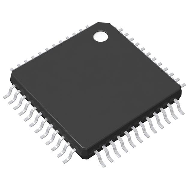


 工商网监
湘ICP备2023018690号
工商网监
湘ICP备2023018690号
