Datasheet
RX23E-A Group
R01DS0330EJ0110
Rev.1.10
Oct 09, 2020
Renesas MCUs
32-MHz, 32-bit RX MCUs with up to 256-KB flash memory,
2 low-noise and low-drift 24-bit delta-sigma A/D converters,
rail-to-rail programmable gain instrumentation amplifiers,
a low-drift voltage reference, and on-chip excitation current sources
Features
■ 32-bit RXv2 CPU core
Max. operating frequency: 32 MHz
Capable of 64 DMIPS in operation at 32 MHz
Enhanced DSP: 32-bit multiply-accumulate and 16-bit multiplysubtract instructions supported
Built-in FPU: 32-bit single-precision floating point (compliant to
IEEE754)
Divider (fastest instruction execution takes two CPU clock cycles)
Fast interrupt
CISC Harvard architecture with 5-stage pipeline
Variable-length instructions, ultra-compact code
On-chip debugging circuit
Memory protection unit (MPU) supported
■ Low power design and architecture
Operation from a single 1.8-V to 5.5-V supply
Three low power consumption modes
Low power timer (LPT) that operates during the software standby state
■ On-chip flash memory for code
Read cycle of 31.25 ns in 32-MHz operation
No waiting time when the CPU is reading at full speed
128-Kbyte to 256-Kbyte capacities
On-board or off-board user programming
Programmable at 1.8 V
For instructions and operands
■ On-chip data flash memory
8 Kbytes (1,000,000 program/erase cycles (typ.))
BGO (Background Operation)
■ On-chip SRAM, no wait states
16- to 32-Kbyte size capacities
■ Data transfer functions
DMAC: Incorporates four channels
DTC: Four transfer modes
■ ELC
Module operation can be initiated by event signals without using
interrupts.
Linked operation between modules is possible while the CPU is
sleeping.
■ Reset and supply management
Seven types of reset, including the power-on reset (POR)
Low voltage detection (LVD) with voltage settings
■ Clock functions
Main clock oscillator frequency: 1 MHz to 20 MHz
External clock input frequency: Up to 20 MHz
PLL circuit input: 4 MHz to 8 MHz
On-chip low- and high-speed oscillators, dedicated on-chip low-speed
oscillator for the IWDT
Clock frequency accuracy measurement circuit (CAC)
■ Independent watchdog timer
15-kHz on-chip oscillator produces a dedicated clock signal to drive
IWDT operation.
■ Useful functions for IEC60730 compliance
Self-diagnostic and disconnect detection assistance functions for the A/
D converter, clock frequency accuracy measurement circuit,
independent watchdog timer, RAM test assistance functions using the
DOC, etc.
■ MPC
Input/output functions selectable from multiple pins
■ Up to eight communication functions
CAN (one channel) compliant to ISO11898-1:
Transfer at up to 1 Mbps
SCI with many useful functions (up to four channels),
asynchronous mode, clock synchronous mode, smart card interface,
reduction of errors in communications using the bit rate modulation
function
I2C bus interface: Transfer at up to 400 kbps, capable of SMBus
operation (one channel)
RSPI (one channel): Transfer at up to 16 Mbps
R01DS0330EJ0110 Rev.1.10
Oct 09, 2020
PLQP0048KB-B
7 × 7 mm, 0.5 mm pitch
PWQN0040KC-A 6 × 6 mm, 0.5 mm pitch
■ Up to 12 extended-function timers
16-bit MTU: input capture, output compare, complementary PWM
output, phase counting mode (six channels)
8-bit TMR (four channels)
16-bit compare-match timers (two channels)
■ Analog functions
Two 24-bit delta-sigma A/D converters
A/D converter with up to 23-bit effective resolution (gain = 1, output
data rate = 7.6 SPS)
High-precision programmable gain instrumentation amplifier,
30 nVRMS (gain = 128, output data rate = 7.6 SPS)
Rail-to-rail programmable gain instrumentation amplifier
(gain = 1 to 128)
Two operating modes and programmable data rates,
Normal mode: Output data rate of 7.6 SPS to 15625 SPS,
Low power mode: Output data rate of 1.9 SPS to 3906 SPS
Offset drift 10 nV/°C (gain = 128)
Gain drift 1 ppm/°C (gain = 1 (PGA), gain = 2 to 128)
Up to six differential inputs, 11 single-ended inputs
Fourth-order sinc filter
Simultaneous 50 Hz/60 Hz rejection (output data rate = 10, 54 SPS)
Offset error and gain error calibration
Inter-unit A/D conversion synchronized start
Delta-sigma A/D input disconnect detection assist
Delta-sigma A/D reference voltage external input
Voltage reference
output voltage: 2.5 V ±0.1%,
temperature drift: 4 ppm/°C, output current: ±10 mA
Excitation current sources: Up to four,
Output current: 50 µA to 1000 µA, current matching: ±0.2%, drift
matching: 5 ppm/°C
Bias voltage generator
output voltage: (AVCC0 + AVSS0)/2
Temperature sensor: Accuracy ±5°C
Low-side switch: 10 Ω on-resistance
Low power-supply-voltage detectors
Delta-sigma A/D input voltage fault detectors
Delta-sigma A/D reference voltage fault detectors and disconnect
detectors
Excitation current source disconnect detectors
■ 12-bit A/D converter
Capable of conversion within 1.4 µs
Six channels
Sampling time can be set for each channel
Self-diagnostic function and analog input disconnect detection
assistance function
■ General I/O ports
5-V tolerant, open drain, input pull-up, switching of driving capacity
■ Operating temperature range
–40°C to +85°C
–40°C to +105°C
■ Applications
General industrial and consumer equipment
Page 1 of 100
�RX23E-A Group
1. Overview
1.
Overview
1.1
Outline of Specifications
Table 1.1 lists the specifications, and Table 1.2 gives a comparison of the functions of the products in different
packages.
Table 1.1 is for products with the greatest number of functions, so the number of peripheral modules and channels will
differ in accordance with the package type. For details, see Table 1.2, Comparison of Functions for Different
Packages.
Table 1.1
Outline of Specifications (1/4)
Classification
Module/Function
Description
CPU
CPU
Memory
Maximum operating frequency: 32 MHz
32-bit RX CPU (RX v2)
Minimum instruction execution time: One instruction per clock cycle
Address space: 4-Gbyte linear
Register set
General purpose: Sixteen 32-bit registers
Control: Ten 32-bit registers
Accumulator: Two 72-bit registers
Basic instructions: 75 (variable-length instruction format)
Floating-point instructions: 11
DSP instructions: 23
Addressing modes: 10
Data arrangement
Instructions: Little endian
Data: Selectable as little endian or big endian
On-chip 32-bit multiplier: 32-bit × 32-bit → 64-bit
On-chip divider: 32-bit ÷ 32-bit → 32 bits
Barrel shifter: 32 bits
Memory protection unit (MPU)
FPU
Single precision (32-bit) floating point
Data types and exceptions in conformance with the IEEE754 standard
ROM
Capacity: 128/256 Kbytes
32 MHz: No-wait access
Programming/erasing method:
Serial programming (asynchronous serial communication), self-programming
RAM
Capacity: 16/32 Kbytes
32 MHz, no-wait memory access
E2 DataFlash
Capacity: 8 Kbytes
Number of erase/write cycles: 1,000,000 (typ)
MCU operating mode
Single-chip mode
Clock
Main clock oscillator, low-speed on-chip oscillator, high-speed on-chip oscillator, PLL
frequency synthesizer, and IWDT-dedicated on-chip oscillator
Oscillation stop detection: Available
Clock frequency accuracy measurement circuit (CAC)
Independent settings for the system clock (ICLK), peripheral module clock (PCLK), and
FlashIF clock (FCLK)
The CPU and system sections such as other bus masters run in synchronization with the
system clock (ICLK): 32 MHz (at max.)
MTU2a runs in synchronization with the PCLKA: 32 MHz (at max.)
The ADCLK for the S12AD runs in synchronization with the PCLKD: 32 MHz (at max.)
Peripheral modules other than MTU2a and S12AD run in synchronization with the
PCLKB: 32 MHz (at max.)
The flash peripheral circuit runs in synchronization with the FCLK: 32 MHz (at max.)
Clock generation circuit
Resets
Voltage
detection
RES# pin reset, power-on reset, voltage monitoring reset, independent watchdog timer
reset, and software reset
Voltage detection circuit
(LVDAb)
R01DS0330EJ0110 Rev.1.10
Oct 09, 2020
When the voltage on VCC falls below the voltage detection level, an internal reset or
internal interrupt is generated.
Voltage detection circuit 0 is capable of selecting the detection voltage from 4 levels
Voltage detection circuit 1 is capable of selecting the detection voltage from 14 levels
Voltage detection circuit 2 is capable of selecting the detection voltage from 4 levels
Page 2 of 100
�RX23E-A Group
Table 1.1
1. Overview
Outline of Specifications (2/4)
Classification
Module/Function
Description
Low power
consumption
Low power consumption
functions
Module stop function
Three low power consumption modes
Sleep mode, deep sleep mode, and software standby mode
Low power timer that operates during the software standby state
Function for lower
operating power
consumption
Operating power control modes
High-speed operating mode and middle-speed operating mode
Interrupt
Interrupt controller
(ICUb)
Interrupt vectors: 256
External interrupts: 9 (NMI, IRQ0 to IRQ7 pins)
Non-maskable interrupts: 5 (NMI pin, oscillation stop detection interrupt, voltage
monitoring 1 interrupt, voltage monitoring 2 interrupt, and IWDT interrupt)
16 levels specifiable for the order of priority
DMA
DMA controller
(DMACA)
4 channels
Three transfer modes: Normal transfer, repeat transfer, and block transfer
Activation sources: Software trigger, external interrupts, and interrupt requests from
peripheral functions
Data transfer controller
(DTCa)
Transfer modes: Normal transfer, repeat transfer, and block transfer
Activation sources: Interrupts
Chain transfer function
General I/O ports
48-pin/40-pin
I/O: 20/16
Input: 1/1
Pull-up resistors: 20/16
Open-drain outputs: 20/16
5-V tolerance: 2/2
I/O ports
Event link controller (ELC)
Event signals of 56 types can be directly connected to the module
Operations of timer modules are selectable at event input
Capable of event link operation for port B
Multi-function pin controller (MPC)
Capable of selecting the input/output function from multiple pins
Timers
Multi-function timer
pulse unit 2 (MTU2a)
(16 bits × 6 channels) × 1 unit
Up to 16 pulse-input/output lines and three pulse-input lines are available based on the
six 16-bit timer channels
Select from among eight or seven counter-input clock signals for each channel (PCLK/1,
PCLK/4, PCLK/16, PCLK/64, PCLK/256, PCLK/1024, MTCLKA, MTCLKB, MTCLKC,
MTCLKD) other than channel 5, for which only four signals are available.
Input capture function
21 output compare/input capture registers
Pulse output mode
PWM/complementary PWM/reset synchronous PWM
Phase-counting mode
Capable of generating conversion start triggers for the A/D converter
Port output enable 2
(POE2a)
Controls the high-impedance state of the MTU’s waveform output pins
Compare match timer
(CMT)
(16 bits × 2 channels) × 1 unit
Select from among four clock signals (PCLK/8, PCLK/32, PCLK/128, PCLK/512)
Independent watchdog
timer (IWDTa)
14 bits × 1 channel
Count clock: Dedicated low-speed on-chip oscillator for the IWDT
Frequency divided by 1, 16, 32, 64, 128, or 256
Low power timer (LPT)
16 bits × 1 channel
Clock source: Dedicated low-speed on-chip oscillator for the IWDT
Frequency divided by 2, 4, 8, 16, or 32
8-bit timer (TMR)
(8 bits × 2 channels) × 2 units
Seven internal clocks (PCLK/1, PCLK/2, PCLK/8, PCLK/32, PCLK/64, PCLK/1024, and
PCLK/8192) and an external clock can be selected
Pulse output and PWM output with any duty cycle are available
Two channels can be cascaded and used as a 16-bit timer
R01DS0330EJ0110 Rev.1.10
Oct 09, 2020
Page 3 of 100
�RX23E-A Group
Table 1.1
Classification
1. Overview
Outline of Specifications (3/4)
Module/Function
Communication Serial communications
functions
interfaces (SCIg, SCIh)
Description
4 channels (channel 1, 5, 6: SCIg, channel 12: SCIh)
SCIg
Serial communications modes: Asynchronous, clock synchronous, and smart-card
interface
Multi-processor function
On-chip baud rate generator allows selection of the desired bit rate
Choice of LSB-first or MSB-first transfer
Average transfer rate clock can be input from TMR timers for SCI5, SCI6, and SCI12
Start-bit detection: Level or edge detection is selectable.
Simple I2C
Simple SPI
9-bit transfer mode
Bit rate modulation
Event linking by the ELC (only on channel 5)
SCIh (The following functions are added to SCIg)
Supports the serial communications protocol, which contains the start frame and
information frame
Supports the LIN format
I2C bus interface
(RIICa)
Serial peripheral
interface (RSPIb)
1 channel
Transfer facility
Using the MOSI (master out, slave in), MISO (master in, slave out), SSL (slave select),
and RSPCK (RSPI clock) enables serial transfer through SPI operation (four lines) or
clock-synchronous operation (three lines)
Capable of handling serial transfer as a master or slave
Data formats
Choice of LSB-first or MSB-first transfer
The number of bits in each transfer can be changed to 8, 9, 10, 11, 12, 13, 14, 15, 16, 20,
24, or 32 bits.
128-bit buffers for transmission and reception
Up to four frames can be transmitted or received in a single transfer operation (with each
frame having up to 32 bits)
Double buffers for both transmission and reception
CAN module (RSCAN)
1 channel
Compliance with the ISO11898-1 specification (standard frame and extended frame)
16 Message boxes
24-bit delta-sigma A/D converter (DSAD)
R01DS0330EJ0110 Rev.1.10
Oct 09, 2020
1 channel
Communications formats: I2C bus format/SMBus format
Master mode or slave mode selectable
Supports fast mode
24 bits (6 channels × 2 units)
Type of A/D conversion: delta-sigma
Post filter: Fourth-order sinc filter
24-bit resolution
Input types: Differential, pseudo-differential, or single-ended
Operating modes
Normal mode/low-power mode
Modulator clock: 500 kHz (typ.; 125 kHz in low-power mode)
Oversampling ratio: 32 to 65536 (only multiples of 16)
Includes a programmable gain instrumentation amplifier (PGA)
Gain settings: ×1, ×2, ×4, ×8, ×16, ×32, ×64, ×128
PGA bypass function: with or without an analog input buffer
Configuration settings per channel
Conditions for starting A/D conversion:
software trigger or ELC
Disconnect detection assist
Selectable reference voltage
Page 4 of 100
�RX23E-A Group
Table 1.1
Classification
1. Overview
Outline of Specifications (4/4)
Module/Function
Description
Analog front end (AFE)
Voltage reference (VREF)
Output voltage: 2.5V
Output from bias voltage source (VBIAS)
Output voltage: (AVCC0 + AVSS0)/2
Internal temperature sensor (TEMPS)
Excitation current sources (IEXC)
Two channels (up to 1000 µA) or four channels (up to 500 µA)
Output current settings: 50 µA, 100 µA, 250 µA, 500 µA, 750 µA, 1000 µA
Analog multiplexer (AMUX)
Select from among external pins, bias voltage sources, internal temperature sensor, or
excitation current sources
Low-side switch (LSW)
On-resistance: 10 Ω (max.)
Allowable current: 30 mA (max.)
Voltage detector (VDET)
Voltage monitoring of AVCC0
Detection of abnormal voltages at analog inputs
Detection of abnormal reference voltages and assistance in detecting disconnection
Assistance in detecting disconnection for excitation current source output
12-bit A/D converter (S12ADE)
12 bits (6 channels × 1 unit)
12-bit resolution
Minimum conversion time: 1.4 µs per channel when the ADCLK is operating at 32 MHz
Operating modes
Scan mode (single scan mode, continuous scan mode, and group scan mode)
Group A priority control (only for group scan mode)
Sampling variable
Sampling time can be set up for each channel.
Self-diagnostic function
Double trigger mode (A/D conversion data duplicated)
Detection of analog input disconnection
A/D conversion start conditions
A software trigger, a trigger from a timer (MTU), an external trigger signal, or ELC
Event linking by the ELC
CRC calculator (CRC)
CRC code generation for arbitrary amounts of data in 8-bit units
Select any of three generating polynomials:
X8 + X2 + X + 1, X16 + X15 + X2 + 1, or X16 + X12 + X5 + 1
Generation of CRC codes for use with LSB-first or MSB-first communications is
selectable.
Data operation circuit (DOC)
Comparison, addition, and subtraction of 16-bit data
Power supply voltages/Operating
frequencies
VCC = 1.8 to 2.4 V: 8 MHz, VCC = 2.4 to 2.7 V: 16 MHz, VCC = 2.7 to 5.5 V: 32 MHz
AVCC0 = 2.7 to 5.5 V (1.8 to 5.5 V when only S12AD is operating)
Operating temperature range
D version: –40 to +85°C, G version: –40 to +105°C
Packages
48-pin LFQFP (PLQP0048KB-B) 7 × 7 mm, 0.5 mm pitch
40-pin HWQFN (PWQN0040KC-A) 6 × 6 mm, 0.5 mm pitch
Debugging interface
One-wire type FINE interface
R01DS0330EJ0110 Rev.1.10
Oct 09, 2020
Page 5 of 100
�RX23E-A Group
Table 1.2
1. Overview
Comparison of Functions for Different Packages
RX23E-A Group
Module/Functions
48 Pins
Interrupts
External interrupts
DMA
DMA controller
40 Pins
NMI, IRQ0 to IRQ7
4 channels (DMAC0 to DMAC3)
Data transfer controller
Timers
Multi-function timer pulse unit 2
Port output enable 2
Communication
functions
Available
6 channels (MTU0 to MTU5)
POE0# to POE3#, POE8#
8-bit timer
2 channels × 2 units
Compare match timer
2 channels × 1 unit
Low power timer
1 channel
Independent watchdog timer
Available
Serial communications interfaces
(SCIg)
3 channels
(SCI1, 5, 6)
Serial communications interfaces
(SCIh)
1 channel (SCI12)
I2C bus interface
1 channel
CAN module
1 channel
Serial peripheral interface
1 channel
24-bit delta-sigma A/D converter
Analog front end
2 channels
(SCI1, 5)
6 channels × 2 units
Voltage reference
Available
Excitation current sources
Available
Analog multiplexer
Available
Temperature sensor
Available
Voltage detector
Available
12-bit A/D converter
(including high-precision channels)
6 channels
(6 channels)
CRC calculator
Available
Event link controller
Packages
R01DS0330EJ0110 Rev.1.10
Oct 09, 2020
4 channels
(4 channels)
Available
48-pin LFQFP
40-pin HWQFN
Page 6 of 100
�RX23E-A Group
1.2
1. Overview
List of Products
Table 1.3 is a list of products, and Figure 1.1 shows how to read the product part no., memory capacity, and package
type.
Table 1.3
List of Products
Group
Part No.
Order Part No.
Package
ROM
Capacity
RAM
Capacity
RX23E-A
R5F523E6ADFL
R5F523E6ADFL#30
PLQP0048KB-B
256 Kbytes
32 Kbytes
R5F523E6ADNF
R5F523E6ADNF#U0
PWQN0040KC-A
R5F523E5ADFL
R5F523E5ADFL#30
PLQP0048KB-B
128 Kbytes
16 Kbytes
R5F523E5ADNF
R5F523E5ADNF#U0
PWQN0040KC-A
R5F523E6AGFL
R5F523E6AGFL#30
PLQP0048KB-B
256 Kbytes
32 Kbytes
R5F523E6AGNF
R5F523E6AGNF#U0
PWQN0040KC-A
R5F523E5AGFL
R5F523E5AGFL#30
PLQP0048KB-B
128 Kbytes
16 Kbytes
256 Kbytes
32 Kbytes
128 Kbytes
16 Kbytes
256 Kbytes
32 Kbytes
128 Kbytes
16 Kbytes
E2
DataFlash
Operating
Frequency
DSAD
Operating
Temperature
–40 to +85°C
2 Units
R5F523E5AGNF
R5F523E5AGNF#U0
PWQN0040KC-A
R5F523E6SDFL
R5F523E6SDFL#30
PLQP0048KB-B
R5F523E6SDNF
R5F523E6SDNF#20
PWQN0040KD-A
R5F523E5SDFL
R5F523E5SDFL#30
PLQP0048KB-B
–40 to +105°C
8 Kbytes
R5F523E5SDNF
R5F523E5SDNF#20
PWQN0040KD-A
R5F523E6SGFL
R5F523E6SGFL#30
PLQP0048KB-B
R5F523E6SGNF
R5F523E6SGNF#20
PWQN0040KD-A
R5F523E5SGFL
R5F523E5SGFL#30
PLQP0048KB-B
R5F523E5SGNF
R5F523E5SGNF#20
PWQN0040KD-A
32 MHz
–40 to +85°C
1 Unit
R01DS0330EJ0110 Rev.1.10
Oct 09, 2020
–40 to +105°C
Page 7 of 100
�RX23E-A Group
R
5
F
1. Overview
5 2
3 E
6
A
D
F L
Package type, number of pins, and pin pitch
FL: LFQFP/48/0.50
NF: HWQFN/40/0.50
Range of ambient temperatures for guaranteed operation
D: Operating ambient temperature: –40 to +85°C
G: Operating ambient temperature: –40 to +105°C
Target sensor
A: Temperature (thermocouple or resistive temperature
detector), DSAD 2 Units
S: Temperature (thermocouple or resistive temperature
detector), DSAD 1 Unit
ROM, RAM, and E2 DataFlash capacity
6: 256 Kbytes/32 Kbytes/8 Kbytes
5: 128 Kbytes/16 Kbytes/8 Kbytes
Group name
3E: RX23E Group
Series name
52: RX200 Series
Type of memory
F: Flash memory version
Renesas MCU
Renesas semiconductor product
Figure 1.1
How to Read the Product Part Number
R01DS0330EJ0110 Rev.1.10
Oct 09, 2020
Page 8 of 100
�RX23E-A Group
1.3
1. Overview
Block Diagram
Figure 1.2 shows a block diagram.
RSCAN
E2 DataFlash
LPT
IWDTa
24-bit delta-sigma A/D converter × 6
channels (unit 0)
ELC
CRC
SCIg × 3 channels
Voltage reference
SCIh × 1 channel
Excitation current sources
Analog multiplexer
Voltage detector
ICUb
ROM
Internal peripheral buses 1 to 6
24-bit delta-sigma A/D converter × 6
channels (unit 1)
RSPIb × 1 channel
RIICa × 1 channel
MTU2a × 6 channels
POE2a
TMR × 2 channels (unit 0)
TMR × 2 channels (unit 1)
CMT × 2 channels (unit 0)
RX CPU
MPU
Clock
generation
circuit
Internal main bus 2
Internal main bus 1
Operand bus
RAM
Instruction bus
12-bit A/D converter × 6 channels
DTCa
DOC
CAC
DMACA
× 4 channels
Port 1
Port 2
Port 3
Port B
Port C
Port H
LVDAb
ICUb:
DTCa:
DMACA:
IWDTa:
ELC:
CRC:
SCIg/SCIh:
RSPIb:
RIICa:
LVDAb:
Figure 1.2
Interrupt controller
Data transfer controller
DMA controller
Independent watchdog timer
Event link controller
CRC (cyclic redundancy check) calculator
Serial communications interface
Serial peripheral interface
I2C bus interface
Voltage detection circuit
MTU2a:
POE2a:
CMT:
DOC:
CAC:
MPU:
TMR:
RSCAN:
LPT:
Multi-function timer pulse unit 2
Port output enable 2
Compare match timer
Data operation circuit
Clock frequency accuracy measurement circuit
Memory protection unit
8-bit timer
CAN module
Low power timer
Block Diagram
R01DS0330EJ0110 Rev.1.10
Oct 09, 2020
Page 9 of 100
�RX23E-A Group
1.4
1. Overview
Pin Functions
Table 1.4 lists the pin functions.
Table 1.4
Pin Functions (1/3)
Classifications
Pin Name
I/O
Description
Power supply
VCC
Input
Power supply pin. Connect it to the system power supply.
VCL
—
Connect this pin to the VSS pin via the 4.7 µF smoothing capacitor used to
stabilize the internal power supply. Place the capacitor close to the pin.
VSS
Input
Ground pin. Connect it to the system power supply (0 V).
XTAL
Output
EXTAL
Input
Pins for connecting a crystal. An external clock can be input through the
EXTAL pin.
CLKOUT
Output
Clock output pin.
Operating mode
control
MD
Input
Pin for setting the operating mode. The signal levels on this pin must not
be changed during operation.
System control
RES#
Input
Reset pin. This MCU enters the reset state when this signal goes low.
Clock
CAC
CACREF
Input
Input pin for the clock frequency accuracy measurement circuit.
On-chip
emulator
FINED
I/O
FINE interface pin.
NMI
Input
Non-maskable interrupt request pin.
IRQ0 to IRQ7
Input
Interrupt request pins.
Multi-function
MTIOC0A, MTIOC0B,
timer pulse unit 2 MTIOC0C, MTIOC0D
I/O
The TGRA0 to TGRD0 input capture input/output compare output/PWM
output pins.
MTIOC1A, MTIOC1B
I/O
The TGRA1 and TGRB1 input capture input/output compare output/PWM
output pins.
MTIOC2A, MTIOC2B
I/O
The TGRA2 and TGRB2 input capture input/output compare output/PWM
output pins.
MTIOC3A, MTIOC3B,
MTIOC3C, MTIOC3D
I/O
The TGRA3 to TGRD3 input capture input/output compare output/PWM
output pins.
MTIOC4A, MTIOC4B,
MTIOC4C, MTIOC4D
I/O
The TGRA4 to TGRD4 input capture input/output compare output/PWM
output pins.
MTIC5U, MTIC5V, MTIC5W
Input
The TGRU5, TGRV5, and TGRW5 input capture input/external pulse input
pins.
MTCLKA, MTCLKB,
MTCLKC, MTCLKD
Input
Input pins for the external clock.
POE0# to POE3#, POE8#
Input
Input pins for request signals to place the MTU pins in the high impedance
state.
Interrupts
Port output
enable 2
8-bit timer
Serial
communications
interface (SCIg)
TMO0 to TMO3
Output
Compare match output pins.
TMCI0 to TMCI3
Input
Input pins for the external clock to be input to the counter.
TMRI0 to TMRI3
Input
Counter reset input pins.
Asynchronous mode/clock synchronous mode
SCK1, SCK5, SCK6
I/O
Input/output pins for the clock.
RXD1, RXD5, RXD6
Input
Input pins for received data.
TXD1, TXD5, TXD6
Output
Output pins for transmitted data.
CTS1#, CTS5#, CTS6#
Input
Input pins for controlling the start of transmission and reception.
RTS1#, RTS5#, RTS6#
Output
Output pins for controlling the start of transmission and reception.
SSCL1, SSCL5, SSCL6
I/O
Input/output pins for the I2C clock.
SSDA1, SSDA5, SSDA6
I/O
Input/output pins for the I2C data.
Simple I2 C mode
R01DS0330EJ0110 Rev.1.10
Oct 09, 2020
Page 10 of 100
�RX23E-A Group
Table 1.4
1. Overview
Pin Functions (2/3)
Classifications
Pin Name
Serial
communications
interface (SCIg)
Simple SPI mode
Serial
communications
interface (SCIh)
I/O
Description
SCK1, SCK5, SCK6
I/O
Input/output pins for the clock.
SMISO1, SMISO5, SMISO6
I/O
Input/output pins for slave transmit data.
SMOSI1, SMOSI5, SMOSI6
I/O
Input/output pins for master transmit data.
SS1#, SS5#, SS6#
Input
Slave-select input pins.
Asynchronous mode/clock synchronous mode
SCK12
I/O
Input/output pin for the clock.
RXD12
Input
Input pin for receiving data.
TXD12
Output
Output pin for transmitting data.
CTS12#
Input
Input pin for controlling the start of transmission and reception.
RTS12#
Output
Output pin for controlling the start of transmission and reception.
SSCL12
I/O
Input/output pin for the I2C clock.
SSDA12
I/O
Input/output pin for the I2C data.
SCK12
I/O
Input/output pin for the clock.
SMISO12
I/O
Input/output pin for slave transmit data.
SMOSI12
I/O
Input/output pin for master transmit data.
SS12#
Input
Slave-select input pin.
RXDX12
Input
Input pin for data reception by SCIh.
TXDX12
Output
Output pin for data transmission by SCIh.
Simple I2C mode
Simple SPI mode
Extended serial mode
I2C bus interface
Serial peripheral
interface
SIOX12
I/O
Input/output pin for data reception or transmission by SCIh.
SCL
I/O
Input/output pin for I2C bus interface clocks. Bus can be directly driven by
the N-channel open drain output.
SDA
I/O
Input/output pin for I2C bus interface data. Bus can be directly driven by
the N-channel open drain output.
RSPCKA
I/O
Input/output pin for the RSPI clock.
MOSIA
I/O
Input/output pin for transmitting data from the RSPI master.
MISOA
I/O
Input/output pin for transmitting data from the RSPI slave.
SSLA0
I/O
Input/output pin to select the slave for the RSPI.
SSLA1 to SSLA3
Output
Output pins to select the slave for the RSPI.
CRXD0
Input
Input pin
CTXD0
Output
Output pin
12-bit A/D converter
AN000 to AN005
Input
Analog input pins for the 12-bit A/D converter.
ADTRG0#
Input
Input pin for the external trigger signal that start the A/D conversion.
Analog front end
REF0P, REF1P
Input
Positive input pins of the reference voltage for the 24-bit delta-sigma A/D
converter.
REF0N, REF1N
Input
Negative input pins of the reference voltage for the 24-bit delta-sigma A/D
converter.
REFOUT
Output
Internal reference voltage output pin.
Connect this to AVSS0 via a capacitor (0.47 µF) for stabilizing the internal
reference voltage. Place the capacitor close to the pin.
IEXC0 to IEXC3
Output
Excitation current source output pins.
CAN module
AIN0 to AIN11
I/O
Analog input/output pins.
LSW
Output
Low-side-switch output pin.
R01DS0330EJ0110 Rev.1.10
Oct 09, 2020
Page 11 of 100
�RX23E-A Group
Table 1.4
1. Overview
Pin Functions (3/3)
Classifications
Pin Name
I/O
Description
Analog power
supply
AVCC0
Input
Analog voltage supply pin. Connect this pin to VCC when not using.
I/O ports
AVSS0
Input
Analog ground pin. Connect this pin to VSS when not using.
VREFH0
Input
Analog reference voltage supply pin for the 12-bit A/D converter.
VREFL0
Input
Analog reference ground pin for the 12-bit A/D converter.
P14 to P17
I/O
4-bit input/output pins.
P26, P27
I/O
2-bit input/output pins.
P30, P31, P35 to P37
I/O
5-bit input/output pins (P35 input pin).
PB0, PB1
I/O
2-bit input/output pins.
PC4 to PC7
I/O
4-bit input/output pins.
PH0 to PH3
I/O
4-bit input/output pins.
R01DS0330EJ0110 Rev.1.10
Oct 09, 2020
Page 12 of 100
�RX23E-A Group
Pin Assignments
Note:
Figure 1.3
LS W
REFOUT
AV SS0
AV CC0
V SS
PB 0
VCC
PB 1
PC4
PC5
PC6
PC7
36
35
34
33
32
31
30
29
28
27
26
25
48-Pin LFQFP
REF0N
37
24
PH0
REF0P
38
23
PH1
AIN0
39
22
PH2
AIN1
40
21
PH3
AIN2
41
20
P14
AIN3
42
19
P15
AIN4/REF1N
43
18
P16
AIN5/REF1P
44
17
P17
AIN6
45
16
P26
AIN7
46
15
P27
AIN8/VREFL0
47
14
P30
AIN9/VREFH0
48
13
P31
1
2
3
4
5
6
7
8
9
10
11
12
AVSS 0
AVCC0
RES #
P 37/XTA L
VS S
P3 6/E XTA L
VCC
VCL
MD
P 35
RX23E-A Group
PLQP0048KB-B
(48-pin LFQFP)
(Top view)
AIN11
1.5.1
AIN10
1.5
1. Overview
This figure indicates the power supply pins and I/O port pins.
For the pin configuration, see the table “List of Pins and Pin Functions (48-Pin LFQFP)”.
Pin Assignments of the 48-Pin LFQFP
R01DS0330EJ0110 Rev.1.10
Oct 09, 2020
Page 13 of 100
�RX23E-A Group
21 PC5
22 PC4
23 PB 1
24 VCC
25 PB 0
26 VS S
PH0
19
PH1
AIN0 33
18
P14
17
P15
16
P16
15
P17
14
P26
13
P27
AIN8/VREFL0 39
12
P30
AIN9/VREFH0 40
11
P31
P35 10
MD 9
V CL
8
VCC 7
4
P3 7/X TAL
6
3
RES#
P36/EX TAL
2
VSS 5
1
AIN7 38
AVSS0
AIN6 37
RX23E-A Group
PWQN0040KC-A
(40-pin HWQFN)
(Top view)
AVCC0
AIN5 /REF1P 36
Figure 1.4
27 AV CC0
20
REF0P 32
AIN4/REF1 N 35
Note:
28 A VSS0
REF0 N 31
AIN1 34
Note:
29 REFOUT
40-Pin HWQFN
30 LS W
1.5.2
1. Overview
This figure indicates the power supply pins and I/O port pins.
For the pin configuration, see the table “List of Pins and Pin Functions (40-Pin HWQFN)”.
It is recommended that the exposed die pad of HWQFN should be connected to VSS.
Pin Assignments of the 40-Pin HWQFN
R01DS0330EJ0110 Rev.1.10
Oct 09, 2020
Page 14 of 100
�RX23E-A Group
1.6
List of Pins and Pin Functions
1.6.1
Table 1.5
Pin
No.
1. Overview
48-Pin LFQFP
List of Pins and Pin Functions (48-Pin LFQFP) (1/2)
Power Supply,
Clock, System
Control
I/O Port
Timers
(MTU, TMR, CMT, POE, CAC)
Communications
(SCIg, SCIh, RSPI, RIIC, CAN)
Analog
(S12AD, VREF,
IEXC, DSAD, AMUX) Others
1
AIN10/AN004/
IEXC0 to IEXC3
2
AIN11/AN005/
IEXC0 to IEXC3
3
AVSS0
4
AVCC0
5
RES#
6
XTAL
7
VSS
8
EXTAL
9
VCC
10
VCL
11
MD
P37
P36
FINED
12
P35
13
P31
MTIOC1A/MTIOC4D/TMO3
CTS1#/RTS1#/SS1#
IRQ1
NMI
14
P30
MTIOC0A/MTIOC4B/TMCI3/
POE8#
RXD1/SMISO1/SSCL1
IRQ0
15
P27
MTIOC2B/MTIOC4A/TMRI3
SCK1
IRQ3
16
P26
MTIOC2A/MTIOC4C/TMO0
TXD1/SMOSI1/SSDA1
IRQ2
17
P17
MTIOC3A/MTIOC3B/TMO1/
POE8#
SCK1/MISOA/SDA
IRQ7
18
P16
MTIOC3C/MTIOC3D/TMO2
TXD1/SMOSI1/SSDA1/MOSIA/
SCL
IRQ6/ADTRG0#
19
P15
MTIOC0B/MTCLKB/TMCI2
RXD1/SMISO1/SSCL1/SSLA1/
CRXD0
IRQ5
20
P14
MTIOC3A/MTCLKA/TMRI2
CTS1#/RTS1#/SS1#/SSLA3/
CTXD0
IRQ4
21
PH3
MTIC5W/MTCLKB/TMCI0/POE2#
CTS6#/RTS6#/SS6#/RSPCKA
22
PH2
MTIC5V/MTCLKA/TMRI0
SCK5/MOSIA
IRQ1
23
PH1
MTIC5U/MTCLKD/TMO0/POE2#
TXD5/SMOSI5/SSDA5/SSLA0
IRQ0/CLKOUT
24
PH0
MTIOC0D/MTCLKC/TMRI0/
CACREF
RXD5/SMISO5/SSCL5/SSLA2
25
PC7
MTIOC3A/MTCLKB/TMO2/
CACREF
TXD6/SMOSI6/SSDA6/MISOA
26
PC6
MTIOC3C/MTCLKA/TMCI2
RXD6/SMISO6/SSCL6/MOSIA
27
PC5
MTIOC3B/MTCLKD/TMRI2
SCK5/SCK6/SCK12/RSPCKA
28
PC4
MTIOC3D/MTCLKC/TMCI1/
POE0#
CTS5#/RTS5#/SS5#/CTS12#/
RTS12#/SS12#/SSLA0
29
PB1
MTIOC1B/MTIOC2A/TMRI1/
POE1#
TXD12/TXDX12/SIOX12/
SMOSI12/SSDA12
PB0
MTIOC0C/TMCI0/POE3#
RXD12/RXDX12/SMISO12/
SSCL12
30
VCC
31
32
VSS
33
AVCC0
34
AVSS0
IRQ4
35
REFOUT
36
LSW
37
REF0N
38
REF0P
39
AIN0/IEXC0 to IEXC3
40
AIN1/IEXC0 to IEXC3
41
AIN2/IEXC0 to IEXC3
R01DS0330EJ0110 Rev.1.10
Oct 09, 2020
Page 15 of 100
�RX23E-A Group
Table 1.5
Pin
No.
1. Overview
List of Pins and Pin Functions (48-Pin LFQFP) (2/2)
Power Supply,
Clock, System
Control
I/O Port
Timers
(MTU, TMR, CMT, POE, CAC)
Communications
(SCIg, SCIh, RSPI, RIIC, CAN)
Analog
(S12AD, VREF,
IEXC, DSAD, AMUX) Others
42
AIN3/IEXC0 to IEXC3
43
AIN4/IEXC0 to
IEXC3/REF1N
44
AIN5/IEXC0 to
IEXC3/REF1P
45
AIN6/AN000/
IEXC0 to IEXC3
46
AIN7/AN001/
IEXC0 to IEXC3
47
VREFL0
AIN8/AN002/
IEXC0 to IEXC3
48
VREFH0
AIN9/AN003/
IEXC0 to IEXC3
R01DS0330EJ0110 Rev.1.10
Oct 09, 2020
Page 16 of 100
�RX23E-A Group
1.6.2
Table 1.6
40-Pin HWQFN
List of Pins and Pin Functions (40-Pin HWQFN)
Pin
No.
Power Supply,
Clock, System
Control
1
AVSS0
2
AVCC0
3
RES#
4
XTAL
5
VSS
6
EXTAL
7
VCC
8
VCL
9
MD
10
1. Overview
I/O Port
Timers
(MTU, TMR, CMT, POE, CAC)
Communications
(SCIg, SCIh, RSPI, RIIC, CAN)
Analog
(S12AD, VREF,
IEXC, DSAD, AMUX) Others
P37
P36
FINED
P35
NMI
11
P31
MTIOC1A/MTIOC4D/TMO3
CTS1#/RTS1#/SS1#
IRQ1
12
P30
MTIOC0A/MTIOC4B/TMCI3/
POE8#
RXD1/SMISO1/SSCL1
IRQ0
13
P27
MTIOC2B/MTIOC4A/TMRI3
SCK1
IRQ3
14
P26
MTIOC2A/MTIOC4C/TMO0
TXD1/SMOSI1/SSDA1
IRQ2
15
P17
MTIOC3A/MTIOC3B/TMO1/
POE8#
SCK1/MISOA/SDA
IRQ7
16
P16
MTIOC3C/MTIOC3D/TMO2
TXD1/SMOSI1/SSDA1/MOSIA/
SCL
IRQ6/ADTRG0#
17
P15
MTIOC0B/MTCLKB/TMCI2
RXD1/SMISO1/SSCL1/SSLA1/
CRXD0
IRQ5
18
P14
MTIOC3A/MTCLKA/TMRI2
CTS1#/RTS1#/SS1#/SSLA3/
CTXD0
IRQ4
IRQ0/CLKOUT
19
PH1
MTCLKD/TMO0/POE2#
TXD5/SMOSI5/SSDA5/SSLA0
20
PH0
MTIOC0D/MTCLKC/TMRI0/
CACREF
RXD5/SMISO5/SSCL5/SSLA2
21
PC5
MTIOC3B/MTCLKD/TMRI2
SCK5/SCK12/RSPCKA
22
PC4
MTIOC3D/MTCLKC/TMCI1/
POE0#
CTS5#/RTS5#/SS5#/CTS12#/
RTS12#/SS12#/SSLA0
23
PB1
MTIOC1B/MTIOC2A/TMRI1/
POE1#
TXD12/TXDX12/SIOX12/
SMOSI12/SSDA12
PB0
MTIOC0C/TMCI0/POE3#
RXD12/RXDX12/SMISO12/
SSCL12
24
VCC
25
26
VSS
27
AVCC0
28
AVSS0
IRQ4
29
REFOUT
30
LSW
31
REF0N
32
REF0P
33
AIN0/IEXC0 to IEXC3
34
AIN1/IEXC0 to IEXC3
35
AIN4/IEXC0 to
IEXC3/REF1N
36
AIN5/IEXC0 to
IEXC3/REF1P
37
AIN6/AN000/
IEXC0 to IEXC3
38
AIN7/AN001/
IEXC0 to IEXC3
39
VREFL0
AIN8/AN002/
IEXC0 to IEXC3
40
VREFH0
AIN9/AN003/
IEXC0 to IEXC3
R01DS0330EJ0110 Rev.1.10
Oct 09, 2020
Page 17 of 100
�RX23E-A Group
2. Electrical Characteristics
2.
Electrical Characteristics
2.1
Absolute Maximum Ratings
Table 2.1
Absolute Maximum Ratings
Conditions: VSS = AVSS0 = VREFL0 = 0 V
Item
Power supply voltage
Input voltage
P16 and P17 (5-V tolerant)
Symbol
Value
Unit
VCC
–0.3 to +6.5
V
–0.3 to +6.5
V
Vin
Ports other than above
Reference power supply voltage
VREFH0
Analog power supply voltage
Analog input voltage
Reference voltage for 24-bit delta-sigma A/D converter
Junction temperature
–0.3 to VCC + 0.3
D version
–0.3 to AVCC0 + 0.3
V
AVCC0
–0.3 to +6.5
V
VAN
–0.3 to AVCC0 + 0.3
V
REF0P, REF1P
–0.3 to AVCC0 + 0.3
V
REF0N, REF1N
–0.3 to AVCC0 + 0.3
Tj
–40 to +105
G version
Storage temperature
°C
–40 to +112
Tstg
–55 to +125
°C
Caution: Exceeding absolute maximum ratings may permanently damage the MCU.
To preclude malfunctions due to noise interference, insert capacitors with high frequency characteristics between the VCC and
VSS pins, between the AVCC0 and AVSS0 pins, and between the VREFH0 and VREFL0 pins. Place capacitors with values of
about 0.1 µF as close as possible to every power supply pin and use the shortest and widest possible traces.
Connect the VCL pin to a VSS pin via a 4.7-µF capacitor. The capacitor must be placed close to the pin. For details, refer to
section 2.12.1, Connecting VCL Capacitor and Bypass Capacitors.
Do not input signals to ports other than 5-V tolerant ports while power is not being supplied to the MCU.
The current injection that results from the input of such a signal may lead to malfunctions and the abnormal current that passes
through the MCU at such times may cause degradation of internal elements.
However, even if –0.3 to +6.5 V is input to a 5-V tolerant port, this will not cause problems such as damage to the MCU.
R01DS0330EJ0110 Rev.1.10
Oct 09, 2020
Page 18 of 100
�RX23E-A Group
2.2
Table 2.2
2. Electrical Characteristics
Recommended Operating Conditions
Recommended Operating Conditions (1)
Item
Power supply voltages
Analog power supply voltages
Operating temperature
D version
Symbol
Min.
Typ.
Max.
Unit
VCC*1, *2
1.8
—
5.5
V
VSS
—
0
—
AVCC0*1, *2
1.8
—
5.5
AVSS0
—
0
—
VREFH0
1.8
—
AVCC0
VREFL0
—
0
—
Topr
–40
—
85
–40
—
105
G version
V
°C
Note 1. Use AVCC0 and VCC under the following conditions:
While VCC > 2.4 V: AVCC0 and VCC can be set independently when AVCC0 ≥ 2.4 V
While VCC ≤ 2.4 V: AVCC0 and VCC can be set independently when AVCC0 ≥ VCC
Note 2. When powering on the VCC and AVCC0 pins, power them on at the same time or the VCC pin first and then the AVCC0 pin.
Table 2.3
Recommended Operating Conditions (2)
Item
VCL pin external capacitance
Symbol
Value
CVCL
4.7 µF ± 30%*1
Note 1. Use a multilayer ceramic capacitor whose nominal capacitance is 4.7 µF and a capacitance tolerance is ±30% or better.
R01DS0330EJ0110 Rev.1.10
Oct 09, 2020
Page 19 of 100
�RX23E-A Group
2.3
2. Electrical Characteristics
DC Characteristics
Table 2.4
DC Characteristics (1)
Conditions: 2.7 V ≤ VCC ≤ 5.5 V, 2.7 V ≤ AVCC0 ≤ 5.5 V, VSS = AVSS0 = 0 V, Ta = –40 to +105°C
Item
Schmitt trigger
input voltage
Symbol
Min.
Typ.
Max.
Unit
VIH
0.7 × VCC
—
5.8
V
P16 and P17 (5-V tolerant)
0.8 × VCC
—
5.8
P14, P15, P26, P27, P30, P31,
P35 to P37, PB0, PB1,
PC4 to PC7, PH0 to PH3, and
RES#
0.8 × VCC
—
VCC + 0.3
VIL
–0.3
—
0.3 × VCC
–0.3
—
0.2 × VCC
ΔVT
0.05 × VCC
—
—
RIIC input pin
(except for SMBus, 5-V tolerant)
RIIC input pin (except for
SMBus)
Other than RIIC input pin
Hysteresis of
Schmitt trigger
input
RIIC input pin (except for
SMBus)
P16 and P17
0.05 × VCC
—
—
Other than RIIC input pin
0.1 × VCC
—
—
0.9 × VCC
—
VCC + 0.3
High-level input
voltage (except for
Schmitt trigger
input pins)
MD
Low-level input
voltage (except for
Schmitt trigger
input pins)
MD
Table 2.5
VIH
EXTAL (external clock input)
RIIC input pin (SMBus)
VIL
0.8 × VCC
—
VCC + 0.3
2.1
—
VCC + 0.3
–0.3
—
0.1 × VCC
EXTAL (external clock input)
–0.3
—
0.2 × VCC
RIIC input pin (SMBus)
–0.3
—
0.8
Test
Conditions
V
DC Characteristics (2)
Conditions: 1.8 V ≤ VCC < 2.7 V, 1.8 V ≤ AVCC0 < 2.7 V, VSS = AVSS0 = 0 V, Ta = –40 to +105°C
Item
Schmitt trigger
input voltage
P16 and P17 (5-V tolerant)
Symbol
Min.
Typ.
Max.
Unit
VIH
0.8 × VCC
—
5.8
V
0.8 × VCC
—
VCC + 0.3
P14, P15, P26, P27, P30, P31,
P35 to P37, PB0, PB1,
PC4 to PC7, PH0 to PH3, and
RES#
P14 to P17, P26, P27, P30, P31,
P35 to P37, PB0, PB1,
PC4 to PC7, PH0 to PH3, and
RES#
VIL
–0.3
—
0.2 × VCC
Hysteresis of
Schmitt trigger
input
P14 to P17, P26, P27, P30, P31,
P35 to P37, PB0, PB1,
PC4 to PC7, PH0 to PH3, and
RES#
ΔVT
0.01 × VCC
—
—
High-level input
voltage (except for
Schmitt trigger
input pins)
MD
VIH
0.9 × VCC
—
VCC + 0.3
0.8 × VCC
—
VCC + 0.3
–0.3
—
0.1 × VCC
–0.3
—
0.2 × VCC
Low-level input
voltage (except for
Schmitt trigger
input pins)
EXTAL (external clock input)
MD
EXTAL (external clock input)
R01DS0330EJ0110 Rev.1.10
Oct 09, 2020
VIL
Test
Conditions
V
Page 20 of 100
�RX23E-A Group
Table 2.6
2. Electrical Characteristics
DC Characteristics (3)
Conditions: 1.8 V ≤ VCC = AVCC0 ≤ 5.5 V, VSS = AVSS0 = 0 V, Ta = –40 to +105°C
Item
Input leakage current
RES#, MD, and P35
Three-state leakage
current (off-state)
P16 and P17
Input capacitance
P14 to P17, P26, P27, P30, P31,
P36, P37, PB0, PB1, PC4 to PC7,
PH0 to PH3, MD, and RES#
Symbol
Min.
Typ.
Max.
Unit
|Iin|
—
—
1.0
µA
Vin = 0 V, VCC
|ITSI|
—
—
1.0
µA
Vin = 0 V, 5.8V
—
—
0.2
Cin
—
—
15
pF
Vin = 20 mV,
f = 1 MHz,
Ta = 25°C
—
—
30
—
2.12
—
V
Ports other than P16 and P17
P35
Output voltage of the VCL pin
Table 2.7
VCL
Test Conditions
Vin = 0 V, VCC
DC Characteristics (4)
Conditions: 1.8 V ≤ VCC = AVCC0 ≤ 5.5 V, VSS = AVSS0 = 0 V, Ta = –40 to +105°C
Item
Input pull-up resistor
Table 2.8
All ports (except for P35)
Symbol
Min.
Typ.
Max.
Unit
RU
10
20
50
kΩ
Test Conditions
Vin = 0 V
DC Characteristics (5)
Conditions: 1.8 V ≤ VCC = AVCC0 ≤ 5.5 V, VSS = AVSS0 = 0 V, Ta = –40 to +105°C
Item
Supply
current
*1
High-speed
operating mode
Normal
operating mode
No peripheral modules
are operating.*2
All peripheral modules
are in normal
operation.
ICLK = 32 MHz
Unit
ICC
4.1
—
mA
2.9
—
ICLK = 8 MHz
2.2
—
ICLK = 4 MHz
1.9
—
MHz*3
16.3
—
ICLK = 16 MHz*3
9.1
—
ICLK = 8 MHz*3
5.5
—
MHz*3
ICLK = 32
3.7
—
ICLK = 32 MHz*3
—
30.3
No peripheral modules
are operating.*2
ICLK = 32 MHz
2.4
—
ICLK = 16 MHz
1.9
—
ICLK = 8 MHz
1.6
—
ICLK = 4 MHz
1.5
—
ICLK = 32 MHz*3
8.9
—
MHz*3
No peripheral modules
are operating.*2
All peripheral modules
are in normal
operation.
5.4
—
ICLK = 8 MHz*3
3.5
—
ICLK = 4 MHz*3
2.5
—
ICLK = 32 MHz
1.5
—
ICLK = 16 MHz
1.3
—
ICLK = 8 MHz
1.2
—
ICLK = 4 MHz
1.2
—
ICLK = 32 MHz*3
7.2
—
ICLK = 16 MHz*3
ICLK = 16
4.4
—
MHz*3
2.8
—
ICLK = 4 MHz*3
2.1
—
2.5
—
ICLK = 8
Increase during BGO
R01DS0330EJ0110 Rev.1.10
Oct 09, 2020
Max.
All peripheral modules
are in full operation.
All peripheral modules
are in normal
operation.
Deep sleep
mode
Typ.
*4
ICLK = 16 MHz
ICLK = 4
Sleep mode
Symbol
operation*5
Test
Conditions
Page 21 of 100
�RX23E-A Group
2. Electrical Characteristics
Symbol
Typ.
*4
Max.
Unit
ICC
2.1
—
mA
ICLK = 8 MHz
1.7
—
ICLK = 4 MHz
1.4
—
ICLK = 1 MHz
1.1
—
Item
Supply
current
*1
Middle-speed
operating mode
Normal
operating mode
No peripheral modules
are operating.*6
All peripheral modules
are in normal
operation.*7
Sleep mode
ICLK = 12 MHz
6.8
—
ICLK = 8 MHz
5.0
—
ICLK = 4 MHz
3.1
—
ICLK = 1 MHz
1.6
—
All peripheral modules
are in full operation.*7
ICLK = 12 MHz
—
13.5
No peripheral modules
are operating.*6
ICLK = 12 MHz
1.4
—
ICLK = 8 MHz
1.2
—
ICLK = 4 MHz
1.1
—
ICLK = 1 MHz
1.0
—
ICLK = 12 MHz
4.0
—
ICLK = 8 MHz
3.0
—
ICLK = 4 MHz
2.1
—
ICLK = 1 MHz
1.3
—
All peripheral modules
are in normal
operation.*7
Deep sleep
mode
ICLK = 12 MHz
No peripheral modules
are operating.*6
All peripheral modules
are in normal
operation.*7
Increase during BGO
operation*5
ICLK = 12 MHz
1.0
—
ICLK = 8 MHz
0.9
—
ICLK = 4 MHz
0.9
—
ICLK = 1 MHz
0.8
—
ICLK = 12 MHz
3.3
—
ICLK = 8 MHz
2.6
—
ICLK = 4 MHz
1.8
—
ICLK = 1 MHz
1.2
—
2.5
—
Test
Conditions
Note 1. Supply current values do not include the output charge/discharge current from all pins. The values apply when internal pull-up
resistors are disabled.
Note 2. Peripheral module clocks are stopped. This does not include BGO operation. The clock source is PLL. FCLK and PCLK are set
to divided by 64.
Note 3. Peripheral module clocks are supplied. This does not include BGO operation. The clock source is PLL. FCLK and PCLK are the
same frequency as that of ICLK.
Note 4. Conditions for typical values are at VCC = 3.3 V and Ta = 25°C.
Note 5. The increase is caused by program/erase operation to the ROM or E2 DataFlash during the execution of a user program.
Note 6. Peripheral module clocks are stopped. The clock source is PLL when ICLK is 12 MHz and HOCO for other cases. FCLK and
PCLK are set to divided by 64.
Note 7. Peripheral module clocks are supplied. The clock source is PLL when ICLK is 12 MHz and HOCO for other cases. FCLK and
PCLK are the same frequency of that of the ICLK.
R01DS0330EJ0110 Rev.1.10
Oct 09, 2020
Page 22 of 100
�RX23E-A Group
2. Electrical Characteristics
40
ICC [mA]
30
Ta = 105°C, ICLK = 32 MHz
20
Ta = 25°C, ICLK = 32 MHz
Ta = 105°C, ICLK = 16 MHz
Ta
Ta
Ta
Ta
Ta
10
= 105°C, ICLK = 8 MHz
= 25°C, ICLK = 16 MHz
= 105°C, ICLK = 4 MHz
= 25°C, ICLK = 8 MHz
= 25°C, ICLK = 4 MHz
0
1.5
2.0
2.5
3.0
3.5
4.0
4.5
5.0
5.5
6.0
VCC [V]
Ta = 25 °C, ICLK = 32 MHz* 1
Ta = 25 °C, ICLK = 16 MHz *
1
Ta = 10 5°C, ICLK = 32 MHz *2
2
Ta = 10 5°C, ICLK = 16 MHz *
Ta = 25 °C, ICLK = 8 MHz * 1
Ta = 10 5°C, ICLK = 8 MHz * 2
Ta = 25 °C, ICLK = 4 MHz * 1
Ta = 10 5°C, ICLK = 4 MHz * 2
Note 1. This result applies when all peripheral modules are in normal operation but BGO is not in use. Indicates the
average of the typical samples through actual measurement during product evaluation.
Note 2. This result applies when all peripheral modules are in full operation but BGO is not in use. Indicates the average
of the upper-limit samples through actual measurement during product evaluation.
Figure 2.1
Voltage Dependence in High-Speed Operating Mode (Reference Data)
R01DS0330EJ0110 Rev.1.10
Oct 09, 2020
Page 23 of 100
�RX23E-A Group
2. Electrical Characteristics
ICC [mA]
20
Ta = 105°C, ICLK = 12 MHz
10
Ta = 105°C, ICLK = 8 MHz
Ta = 25°C, ICLK = 12 MHz
Ta = 105°C, ICLK = 4 MHz
Ta = 25°C, ICLK = 8 MHz
Ta = 25°C, ICLK = 4 MHz
Ta = 105°C, ICLK = 1 MHz
Ta = 25°C, ICLK = 1 MHz
0
1.5
2.0
2.5
3.0
3.5
4.0
VCC [V]
Ta = 25°C, ICLK = 12 MHz *
1
1
4.5
5.0
5.5
6.0
Ta = 105°C, ICLK = 12 MHz *
2
Ta = 25°C, ICLK = 8 MHz *
Ta = 105°C, ICLK = 8 MHz *
Ta = 25°C, ICLK = 4 MHz *1
Ta = 105°C, ICLK = 4 MHz * 2
1
Ta = 25°C, ICLK = 1 MHz *
Ta = 105°C, ICLK = 1 MHz *
2
2
Note 1. This result applies when all peripheral modules are in normal operation but BGO is not in use. Indicates the
average of the typical samples through actual measurement during product evaluation.
Note 2. This result applies when all peripheral modules are in full operation but BGO is not in use. Indicates the average
of the upper-limit samples through actual measurement during product evaluation.
Figure 2.2
Voltage Dependence in Middle-Speed Operating Mode (Reference Data)
R01DS0330EJ0110 Rev.1.10
Oct 09, 2020
Page 24 of 100
�RX23E-A Group
Table 2.9
2. Electrical Characteristics
DC Characteristics (6)
Conditions: 1.8 V ≤ VCC = AVCC0 ≤ 5.5 V, VSS = AVSS0 = 0 V, Ta = –40 to +105°C
Symbol
Typ.*3
Max.
Unit
ICC
0.4
2.6
µA
Ta = 55°C
0.8
3.0
Ta = 85°C
2.5
12.6
Ta = 105°C
6.3
31.2
Increment for IWDT operation
0.4
—
Increment for LPT operation
0.4
—
Item
Supply
current*1
Software standby
mode*2
Ta = 25°C
Test Conditions
Use IWDT-Dedicated On-Chip Oscillator for
clock source
Note 1. Supply current values were obtained with no load on any output pin and all internal pull-up resistors disabled.
Note 2. The IWDT and LVD are stopped.
Note 3. Conditions for typical values are at VCC = 3.3 V.
100
2
Ta = 105°C *
10
2
ICC [µA]
Ta = 85°C *
1
Ta = 105°C *
1
Ta = 85°C *
2
Ta = 55°C *
1
1
Ta = 55°C *
2
Ta = 25°C *
1
Ta = 25°C *
0.1
1.5
2.0
2.5
3.0
3.5
4.0
4.5
5.0
5.5
6.0
VCC [V]
Ta = 25°C *1
2
Ta = 25°C *
Ta = 55°C *1
2
Ta = 55°C *
Ta = 85°C *1
2
Ta = 85°C *
Ta = 105°C *1
2
Ta = 105°C *
Note 1. Indicates the average of the typical samples through actual measurement during product evaluation.
Note 2. Indicates the average of the upper-limit samples through actual measurement during product evaluation.
Figure 2.3
Voltage Dependence in Software Standby Mode (Reference Data)
R01DS0330EJ0110 Rev.1.10
Oct 09, 2020
Page 25 of 100
�RX23E-A Group
2. Electrical Characteristics
100
ICC [µA]
10
1
0.1
–40
–20
0
20
40
60
80
100
Ta [°C]
Average value of the tested middle samples during product evaluation.
Average value of the tested upper-limit samples during product evaluation.
Figure 2.4
Table 2.10
Temperature Dependence in Software Standby Mode (Reference Data)
DC Characteristics (7)
Conditions: 1.8 V ≤ VCC = AVCC0 ≤ 5.5 V, VSS = AVSS0 = 0 V, Ta = –40 to +105°C
Symbol
Min.
Typ.*1
Max.
Unit
lLVD
—
0.10
—
µA
LVD1
—
0.10
—
LVD2
—
0.20
—
Item
LVD
LVD0
Test Conditions
Note 1. Conditions for typical values are at VCC = AVCC0 = 3.3 V and Ta = 25°C.
Table 2.11
DC Characteristics (8)
Conditions: 1.8 V ≤ VCC = AVCC0 ≤ 5.5 V, VSS = AVSS0 = 0 V, Ta = –40 to +105°C
Item
RAM standby voltage
Table 2.12
Symbol
Min.
Typ.
Max.
Unit
VRAM
1.8
—
—
V
Test Conditions
DC Characteristics (9)
Conditions: 0 V ≤ VCC = AVCC0 ≤ 5.5 V, VSS = AVSS0 = 0 V, Ta = –40 to +105°C
Item
VCC ramp-up rate at
power-on
Note 1.
Note 2.
Note 3.
Note 4.
Symbol
Min.
Typ.
Max.
Unit
SrVCC
0.02
—
20.00
ms/V
During fast startup time*2
0.02
—
2.00
Voltage monitoring 0 reset
enabled at startup*3, *4
0.02
—
—
At normal startup*1
Test Conditions
When the OFS1.LVDAS and OFS1.FASTSTUP bits are 1
When the OFS1.LVDAS bit is 1 and the OFS1.FASTSTUP bit is 0
When the OFS1.LVDAS bit is 0
Turn on the power supply voltage according to the normal startup rising gradient because the settings in the OFS1 register are
not read in boot mode.
R01DS0330EJ0110 Rev.1.10
Oct 09, 2020
Page 26 of 100
�RX23E-A Group
Table 2.13
2. Electrical Characteristics
DC Characteristics (10)
Conditions: 1.8 V ≤ VCC = AVCC0 ≤ 5.5 V, VSS = AVSS0 = 0 V, Ta = –40 to +105°C
The result of any ripple must be within the limit on allowable ripple frequency fr (VCC) where the ripple voltage is within the range
between the VCC upper limit and lower limit. The result of any ripple must be within the limit on the allowable VCC ramp rate in
power fluctuation (dt/dVCC) where the change in VCC exceeds VCC ±10%.
Item
Allowable ripple frequency
Allowable VCC ramp rate at
power fluctuation
Symbol
Min.
Typ.
Max.
Unit
fr (VCC)
—
—
10
kHz
Figure 2.5
Vr (VCC) ≤ 0.2 × VCC
—
—
1
MHz
Figure 2.5
Vr (VCC) ≤ 0.08 × VCC
—
—
10
MHz
Figure 2.5
Vr (VCC) ≤ 0.06 × VCC
1.0
—
—
ms/V
When VCC change exceeds VCC ±10%
dt/dVCC
Test Conditions
1 / fr (VCC)
VCC
Figure 2.5
Vr (VCC)
Ripple Waveform
R01DS0330EJ0110 Rev.1.10
Oct 09, 2020
Page 27 of 100
�RX23E-A Group
Table 2.14
2. Electrical Characteristics
DC Characteristics (11)
Conditions: 1.8 V ≤ VCC ≤ 5.5 V, 2.7 V ≤ AVCC0 ≤ 5.5 V, VSS = AVSS0 = 0 V, Ta = –40 to +105°C
Item
Operating current of
24-bit delta-sigma
A/D converter
(normal mode)
Operating current of
24-bit delta-sigma
A/D converter
(low power mode)
Symbol
Min.
Typ.
Max.
Unit
IAVCC0
—
500*1
660
µA
Gain = 1 to 16 (PGA enabled)
OPCR.DSADLVM bit = 0
—
840*1
1130
Gain = 32 to 128
OPCR.DSADLVM bit = 0
—
1050*1
1360
Gain = 1
(PGA disabled, BUF disabled)
OPCR.DSADLVM bit = 1
—
490*2
850
Gain = 1 to 16 (PGA enabled)
OPCR.DSADLVM bit = 1
—
820*2
1320
Gain = 32 to 128
OPCR.DSADLVM bit = 1
—
1040*2
1560
Gain = 1
(PGA disabled, BUF disabled)
OPCR.DSADLVM bit = 0
—
250*1
280
Gain = 1 to 16 (PGA enabled)
OPCR.DSADLVM bit = 0
—
390*1
480
Gain = 32 to 128
OPCR.DSADLVM bit = 0
—
430*1
520
Gain = 1
(PGA disabled, BUF disabled)
OPCR.DSADLVM bit = 1
—
240*2
350
Gain = 1 to 16 (PGA enabled)
OPCR.DSADLVM bit = 1
—
380*2
550
Gain = 32 to 128
OPCR.DSADLVM bit = 1
—
420*2
590
—
45
75
µA
Figure 2.18
—
15
40
µA
Figure 2.19
—
15
25
µA
Figure 2.20
—
55
70
µA
Figure 2.21
µA
Gain = 1
(PGA disabled, BUF disabled)
OPCR.DSADLVM bit = 0
Operating current of voltage reference
(DSAD)
IAVCC0
Test Conditions
Figure 2.6, Figure 2.7
1 unit, external reference
in use, reference buffer
disabled,
AVCC0 = 3.6 to 5.5 V
Figure 2.8, Figure 2.9
1 unit, external reference
in use, reference buffer
disabled,
AVCC0 = 2.7 to 5.5 V
µA
Figure 2.10, Figure 2.11
1 unit, external reference
in use, reference buffer
disabled,
AVCC0 = 3.6 to 5.5 V
Figure 2.12, Figure 2.13
1 unit, external reference
in use, reference buffer
disabled,
AVCC0 = 2.7 to 5.5 V
(VREF)
Operating current of temperature sensor
IAVCC0
(TEMPS)
Operating current of bias voltage generator
IAVCC0
(VBIAS)
Operating current of excitation current source
IAVCC0
(IEXC)
Operating current of
analog input buffer
Normal mode
Operating current of
reference buffer
Normal mode
Operating current of
voltage detector
Low voltage detector for
power supply
(LVDET)
Excitation current source
disconnect detector
(IEXCDET)
DSAD input voltage fault
detector
(DSIDET)
DSAD reference voltage fault
detector
(DSRDET)
Low power mode
Low power mode
IAVCC0
—
85
130
(BUF)
—
25
40
IAVCC0
—
85
130
(REFBUF)
—
25
40
IAVCC0
—
5
9
—
1
2
—
5
7
—
10
15
IAVCC0
IAVCC0
IAVCC0
Figure 2.14, 1 unit
Figure 2.15, 1 unit
µA
Figure 2.16, 1 unit
Figure 2.17, 1 unit
µA
1 unit
Note 1. Conditions for this value is at AVCC0 = 5.0 V and Ta = 25°C.
Note 2. Conditions for this value is at AVCC0 = 3.3 V and Ta = 25°C.
R01DS0330EJ0110 Rev.1.10
Oct 09, 2020
Page 28 of 100
�2. Electrical Characteristics
1400
1400
1200
1200
1000
800
600
400
Gain = 1
(PGA disabled, BUF disabled)
Gain = 16
Gain = 128
200
0
–50
–25
0
25
50
75
100
AVCC0 current [µA]
AVCC0 current [µA]
RX23E-A Group
1000
800
600
400
Gain = 1
(PGA disabled, BUF disabled)
Gain = 16
Gain = 128
200
0
3.0
125
3.5
Temperature [°C]
Figure 2.7
1400
1400
1200
1200
1000
800
600
400
Gain = 1
(PGA disabled, BUF disabled)
Gain = 16
Gain = 128
200
0
–50
600
400
Gain = 1
(PGA disabled, BUF disabled)
Gain = 16
Gain = 128
200
0
–25
0
25
50
75
100
125
2.5
3.0
Figure 2.9
500
500
400
300
200
Gain = 1
(PGA disabled, BUF disabled)
Gain = 16
Gain = 128
100
3.5
4.0
4.5
5.0
5.5
6.0
AVCC0 [V]
Temperature Dependence of Operating
Current of 24-Bit Delta-Sigma A/D
Converter (AVCC0 = 5.0 V, Normal Mode,
OPCR.DSADLVM bit = 1)
AVCC0 current [µA]
AVCC0 current [µA]
6.0
800
600
Power-Supply Voltage Dependence of
Operating Current of 24-Bit Delta-Sigma
A/D Converter (Ta = 25°C, Normal Mode,
OPCR.DSADLVM bit = 1)
400
300
200
Gain = 1
(PGA disabled, BUF disabled)
Gain = 16
Gain = 128
100
0
–25
0
25
50
75
100
125
3.0
Temperature Dependence of Operating
Current of 24-Bit Delta-Sigma A/D
Converter (AVCC0 = 5.0 V, Low Power
Mode, OPCR.DSADLVM bit = 0)
R01DS0330EJ0110 Rev.1.10
Oct 09, 2020
3.5
4.0
4.5
5.0
5.5
6.0
AVCC0 [V]
Temperature [°C]
Figure 2.10
5.5
1000
600
0
–50
5.0
Power-Supply Voltage Dependence of
Operating Current of 24-Bit Delta-Sigma
A/D Converter (Ta = 25°C, Normal Mode,
OPCR.DSADLVM bit = 0)
Temperature [°C]
Figure 2.8
4.5
AVCC0 [V]
Temperature Dependence of Operating
Current of 24-Bit Delta-Sigma A/D
Converter (AVCC0 = 5.0 V, Normal Mode,
OPCR.DSADLVM bit = 0)
AVCC0 current [µA]
AVCC0 current [µA]
Figure 2.6
4.0
Figure 2.11
Power-Supply Voltage Dependence of
Operating Current of 24-Bit Delta-Sigma
A/D Converter (Ta = 25°C, Low Power
Mode, OPCR.DSADLVM bit = 0)
Page 29 of 100
�2. Electrical Characteristics
600
600
500
500
400
300
200
Gain = 1
(PGA disabled, BUF disabled)
Gain = 16
Gain = 128
100
0
–50
AVCC0 current [µA]
AVCC0 current [µA]
RX23E-A Group
400
300
200
Gain = 1
(PGA disabled, BUF disabled)
Gain = 16
Gain = 128
100
0
–25
0
25
50
75
100
125
2.5
3.0
3.5
Temperature Dependence of Operating
Current of 24-Bit Delta-Sigma A/D
Converter (AVCC0 = 5.0 V, Low Power
Mode, OPCR.DSADLVM bit = 1)
Figure 2.13
100
70
AVCC0 = 3.3 V
AVCC0 = 5.0 V
60
AVCC0 current [µA]
80
50
–50 –25
AVCC0 = 3.3 V
AVCC0 = 5.0 V
0
25
50
75
AVCC0 = 5.5 V
10
–50 –25
100 125 150
0
25
50
75
100 125 150
Temperature [°C]
Temperature Dependence of Operating
Current of Analog Input Buffer
(Normal Mode)
Figure 2.15
Temperature Dependence of Operating
Current of Analog Input Buffer
(Low Power Mode)
30
90
80
70
AVCC0 = 3.3 V
60
50
–50 –25
0
25
50
AVCC0 current [µA]
100
AVCC0 current [µA]
6.0
20
Temperature [°C]
20
AVCC0 = 3.3 V
AVCC0 = 5.0 V
AVCC0 = 5.0 V
AVCC0 = 5.5 V
AVCC0 = 5.5 V
75
100 125 150
10
–50 –25
Temperature [°C]
Figure 2.16
5.5
Power-Supply Voltage Dependence of
Operating Current of 24-Bit Delta-Sigma
A/D Converter (Ta = 25°C, Low Power
Mode, OPCR.DSADLVM bit = 1)
AVCC0 = 5.5 V
Figure 2.14
5.0
30
90
AVCC0 current [µA]
4.5
AVCC0 [V]
Temperature [°C]
Figure 2.12
4.0
Temperature Dependence of Operating
Current of Reference Buffer
(Normal Mode)
R01DS0330EJ0110 Rev.1.10
Oct 09, 2020
0
25
50
75
100 125 150
Temperature [°C]
Figure 2.17
Temperature Dependence of Operating
Current of Reference Buffer
(Low Power Mode)
Page 30 of 100
�RX23E-A Group
2. Electrical Characteristics
20
AVCC0 current [µA]
AVCC0 current [µA]
60
50
40
AVCC0 = 2.7 V
AVCC0 = 3.3 V
30
10
AVCC0 = 2.7 V
AVCC0 = 3.3 V
AVCC0 = 5.0 V
AVCC0 = 5.0 V
AVCC0 = 5.5 V
AVCC0 = 5.5 V
20
–50 –25
0
25
50
75
100
125
0
–50 –25
150
0
Temperature [°C]
Figure 2.18
50
75
Figure 2.19
AVCC0 current [µA]
AVCC0 = 2.7 V
10
Temperature Dependence of Operating
Current of Temperature Sensor
AVCC0 = 3.3 V
60
AVCC0 = 2.7 V
50
AVCC0 = 3.3 V
AVCC0 = 5.0 V
AVCC0 = 5.0 V
AVCC0 = 5.5 V
–25
0
25
50
75
100 125
AVCC0 = 5.5 V
150
40
–50 –25
Temperature [°C]
Figure 2.20
125 150
70
20
0
–50
100
Temperature [°C]
Temperature Dependence of Operating
Current of Voltage Reference
30
AVCC0 current [µA]
25
Temperature Dependence of Operating
Current of Bias Voltage Generator
R01DS0330EJ0110 Rev.1.10
Oct 09, 2020
0
25
50
75
100 125
150
Temperature [°C]
Figure 2.21
Temperature Dependence of Operating
Current of Excitation Current Source
Page 31 of 100
�RX23E-A Group
Table 2.15
2. Electrical Characteristics
DC Characteristics (12)
Conditions: 1.8 V ≤ VCC ≤ 5.5 V, 1.8 V ≤ AVCC0 ≤ 5.5 V, VSS = AVSS0 = 0 V, Ta = –40 to +105°C
12-bit A/D converter
operating current
Item
Symbol
Min.
Typ.*1
Max.
Unit
During A/D conversion
(in high-speed conversion)
IAVCC0
—
1.1
1.8
mA
—
0.6
1.1
—
71
122
µA
—
—
60
nA
—
—
2.2
µA
(S12AD)
During A/D conversion
(in low-current mode)
Reference power
supply current
Test Conditions
During A/D conversion
(in high-speed conversion)
IREFH0
Current while waiting for A/D
conversion (all units)
AVCC0 power down current
ISTBY
Note 1. Conditions for typical values are at AVCC0 = 5.0 V and Ta = 25°C.
Table 2.16
Permissible Output Currents (1)
Conditions: 1.8 V ≤ VCC = AVCC0 ≤ 5.5 V, VSS = AVSS0 = 0 V, Ta = –40 to +85°C
Item
Permissible low-level output
current (average value per pin)
P36 and P37
Ports other than above
Symbol
Max.
Unit
IOL
4.0
mA
Normal drive output mode
4.0
High-drive output mode
Permissible low-level output
current (maximum value per pin)
P36 and P37
Permissible low-level output
current
Total of P14 to P17, P26, P27, P30, P31, P36, and P37
Ports other than above
8.0
4.0
Normal drive output mode
4.0
High-drive output mode
8.0
ΣIOL
Total of PB0, PB1, PC4 to PC7, and PH0 to PH3
40
Total of all output pins
Permissible high-level output
current (average value per pin)
80
P36 and P37
Ports other than above
IOH
Normal drive output mode
P36 and P37
Permissible high-level output
current
Total of P14 to P17, P26, P27, P30, P31, P36, and P37
–8.0
–4.0
Normal drive output mode
–4.0
High-drive output mode
R01DS0330EJ0110 Rev.1.10
Oct 09, 2020
–4.0
–4.0
High-drive output mode
Permissible high-level output
current (maximum value per pin)
Ports other than above
40
–8.0
ΣIOH
–40
Total of PB0, PB1, PC4 to PC7, and PH0 to PH3
–40
Total of all output pins
–80
Page 32 of 100
�RX23E-A Group
Table 2.17
2. Electrical Characteristics
Permissible Output Currents (2)
Conditions: 1.8 V ≤ VCC = AVCC0 ≤ 5.5 V, VSS = AVSS0 = 0 V, Ta = –40 to +105°C
Item
Permissible low-level output
current (average value per pin)
Symbol
Max.
Unit
IOL
4.0
mA
P36 and P37
Ports other than above
Normal drive output mode
4.0
High-drive output mode
Permissible low-level output
current (maximum value per pin)
P36 and P37
Permissible low-level output
current
Total of P14 to P17, P26, P27, P30, P31, P36, and P37
Ports other than above
8.0
4.0
Normal drive output mode
4.0
High-drive output mode
Permissible high-level output
current (average value per pin)
30
Total of all output pins
60
Ports other than above
Permissible high-level output
current
30
Total of PB0, PB1, PC4 to PC7, and PH0 to PH3
P36 and P37
Permissible high-level output
current (maximum value per pin)
Table 2.18
8.0
ΣIOL
–4.0
IOH
Normal drive output mode
–4.0
High-drive output mode
–8.0
P36 and P37
Ports other than above
–4.0
Normal drive output mode
–4.0
High-drive output mode
–8.0
ΣIOH
Total of P14 to P17, P26, P27, P30, P31, P36, and P37
–30
Total of PB0, PB1, PC4 to PC7, and PH0 to PH3
–30
Total of all output pins
–60
Output Voltage (1)
Conditions: 1.8 V ≤ VCC = AVCC0 < 2.7 V, VSS = AVSS0 = 0 V, Ta = –40 to +105°C
Item
Low-level output
voltage
All output ports
Normal drive output mode
High-level output
voltage
All output ports
Normal drive output mode
Table 2.19
Symbol
Min.
Max.
Unit
VOL
—
0.3
V
IOL = 0.5 mA
—
0.3
VOH
VCC – 0.3
—
V
IOH = –0.5 mA
VCC – 0.3
—
High-drive output mode
High-drive output mode
Test Conditions
IOL = 1.0 mA
IOH = –1.0 mA
Output Voltage (2)
Conditions: 2.7 V ≤ VCC = AVCC0 < 4.0 V, VSS = AVSS0 = 0 V, Ta = –40 to +105°C
Item
Low-level output
voltage
Symbol
Min.
Max.
Unit
VOL
—
0.5
V
High-drive output mode
—
0.5
IOL = 2.0 mA
RIIC pins
Normal drive output mode
—
0.4
IOL = 3.0 mA
All output ports
Normal drive output mode
All output ports
(except for RIIC
pins)
Normal drive output mode
High-drive output mode
High-level output
voltage
R01DS0330EJ0110 Rev.1.10
Oct 09, 2020
High-drive output mode
VOH
—
0.6
VCC – 0.5
—
VCC – 0.5
—
Test Conditions
IOL = 1.0 mA
IOL = 6.0 mA
V
IOH = –1.0 mA
IOH = –2.0 mA
Page 33 of 100
�RX23E-A Group
Table 2.20
2. Electrical Characteristics
Output Voltage (3)
Conditions: 4.0 V ≤ VCC = AVCC0 ≤ 5.5 V, VSS = AVSS0 = 0 V, Ta = –40 to +105°C
Item
Low-level output
voltage
Symbol
Min.
Max.
Unit
VOL
—
0.8
V
High-drive output mode
—
0.8
IOL = 4.0 mA
RIIC pins
Normal drive output mode
—
0.4
IOL = 3.0 mA
All output ports
Normal drive output mode
All output ports
(except for RIIC
pins)
Normal drive output mode
High-drive output mode
High-level output
voltage
Table 2.21
High-drive output mode
VOH
—
0.6
VCC – 0.8
—
VCC – 0.8
—
IOL = 6.0 mA
V
IOH = –2.0 mA
IOH = –4.0 mA
Thermal Resistance Value (Reference)
Item
Thermal resistance
Package
48-pin LFQFP (PLQP0048KB-B)
Symbol
Max.
Unit
ja
50.7
°C/W
JESD51-2 and
JESD51-7 compliant
°C/W
JESD51-2 and
JESD51-7 compliant
40-pin HWQFN (PWQN0040KC-A)
48-pin LFQFP (PLQP0048KB-B)
40-pin HWQFN (PWQN0040KC-A)
Note:
Test Conditions
IOL = 2.0 mA
18.8
jt
1.07
0.07
Test Conditions
The values are reference values when the 4-layer board is used. Thermal resistance depends on the number of layers or size of
the board. For details, refer to the JEDEC standards.
R01DS0330EJ0110 Rev.1.10
Oct 09, 2020
Page 34 of 100
�RX23E-A Group
2.3.1
2. Electrical Characteristics
Typical I/O Pin Output Characteristics (1)
Figure 2.22 to Figure 2.26 show the characteristics when normal drive output is selected by the drive capacity control
register.
IOH/IOL vs VOH/VOL
50
VCC = 5.5V
40
30
VCC = 3.3V
20
VCC = 2.7V
IOH/IOL [mA]
10
VCC = 1.8V
0
VCC = 1.8V
–10
VCC = 2.7V
–20
VCC = 3.3V
–30
–40
–50
VCC = 5.5V
–60
0
1
2
3
4
5
6
VOH/VOL [V]
Figure 2.22
VOH/VOL and IOH/IOL Voltage Characteristics at Ta = 25°C When Normal Drive Output is Selected
(Reference Data)
IOH/IOL vs VOH/VOL
8
6
Ta = –40°C
Ta = 25°C
IOH/IOL [mA]
4
Ta = 105°C
2
0
–2
Ta = 105°C
–4
Ta = 25°C
Ta = –40°C
–6
–8
0.0
0.2
0.4
0.6
0.8
1.0
1.2
1.4
1.6
1.8
2.0
VOH/VOL [V]
Figure 2.23
VOH/VOL and IOH/IOL Temperature Characteristics at VCC = 1.8 V When Normal Drive Output is
Selected (Reference Data)
R01DS0330EJ0110 Rev.1.10
Oct 09, 2020
Page 35 of 100
�RX23E-A Group
2. Electrical Characteristics
IOH/IOL vs VOH/VOL
20
15
Ta = –40°C
Ta = 25°C
IOH/IOL [mA]
10
Ta = 105°C
5
0
–5
–10
Ta = 105°C
Ta = 25°C
–15
Ta = –40°C
–20
0.0
0.5
1.0
1.5
2.0
2.5
3.0
VOH/VOL [V]
Figure 2.24
VOH/VOL and IOH/IOL Temperature Characteristics at VCC = 2.7 V When Normal Drive Output is
Selected (Reference Data)
IOH/IOL vs VOH/VOL
30
Ta = –40°C
20
Ta = 25°C
Ta = 105°C
IOH/IOL [mA]
10
0
–10
Ta = 105°C
–20 Ta = 25°C
Ta = –40°C
–30
0.0
0.5
1.0
1.5
2.0
2.5
3.0
3.5
VOH/VOL [V]
Figure 2.25
VOH/VOL and IOH/IOL Temperature Characteristics at VCC = 3.3 V When Normal Drive Output is
Selected (Reference Data)
R01DS0330EJ0110 Rev.1.10
Oct 09, 2020
Page 36 of 100
�RX23E-A Group
2. Electrical Characteristics
IOH/IOL vs VOH/VOL
60
Ta = –40°C
Ta = 25°C
Ta = 105°C
40
IOH/IOL [mA]
20
0
–20
–40
Ta = 105°C
Ta = 25°C
Ta = –40°C
–60
0
1
2
3
4
5
6
VOH/VOL [V]
Figure 2.26
VOH/VOL and IOH/IOL Temperature Characteristics at VCC = 5.5 V When Normal Drive Output is
Selected (Reference Data)
R01DS0330EJ0110 Rev.1.10
Oct 09, 2020
Page 37 of 100
�RX23E-A Group
2.3.2
2. Electrical Characteristics
Typical I/O Pin Output Characteristics (2)
Figure 2.27 to Figure 2.31 show the characteristics when high-drive output is selected by the drive capacity control
register.
IOH/IOL vs VOH/VOL
150
VCC = 5.5V
100
VCC = 3.3V
50
IOH/IOL [mA]
VCC = 2.7V
VCC = 1.8V
0
VCC = 1.8V
VCC = 2.7V
–50
VCC = 3.3V
–100
VCC = 5.5V
–150
0
1
2
3
4
5
6
VOH/VOL [V]
Figure 2.27
VOH/VOL and IOH/IOL Voltage Characteristics at Ta = 25°C When High-Drive Output is Selected
(Reference Data)
IOH/IOL vs VOH/VOL
16
12
Ta = –40°C
Ta = 25°C
Ta = 105°C
IOH/IOL [mA]
8
4
0
–4
–8
Ta = 105°C
Ta = 25°C
–12
Ta = –40°C
–16
0.0
0.2
0.4
0.6
0.8
1.0
1.2
1.4
1.6
1.8
2.0
VOH/VOL [V]
Figure 2.28
VOH/VOL and IOH/IOL Temperature Characteristics at VCC = 1.8 V When High-Drive Output is
Selected (Reference Data)
R01DS0330EJ0110 Rev.1.10
Oct 09, 2020
Page 38 of 100
�RX23E-A Group
2. Electrical Characteristics
IOH/IOL vs VOH/VOL
50
40
Ta = –40°C
30
Ta = 25°C
Ta = 105°C
IOH/IOL [mA]
20
10
0
–10
–20
Ta = 105°C
Ta = 25°C
Ta = –40°C
–30
–40
–50
0.0
1.0
0.5
1.5
3.0
2.5
2.0
VOH/VOL [V]
Figure 2.29
VOH/VOL and IOH/IOL Temperature Characteristics at VCC = 2.7 V When High-Drive Output is
Selected (Reference Data)
IOH/IOL vs VOH/VOL
60
Ta = –40°C
Ta = 25°C
40
Ta = 105°C
IOH/IOL [mA]
20
0
–20
Ta = 105°C
–40 Ta = 25°C
Ta = –40°C
–60
0.0
0.5
1.0
1.5
2.0
2.5
3.0
3.5
VOH/VOL [V]
Figure 2.30
VOH/VOL and IOH/IOL Temperature Characteristics at VCC = 3.3 V When High-Drive Output is
Selected (Reference Data)
R01DS0330EJ0110 Rev.1.10
Oct 09, 2020
Page 39 of 100
�RX23E-A Group
2. Electrical Characteristics
IOH/IOL vs VOH/VOL
150
Ta = –40°C
Ta = 25°C
Ta = 105°C
100
IOH/IOL [mA]
50
0
–50
Ta = 105°C
–100
Ta = 25°C
Ta = –40°C
–150
0
1
2
3
4
6
5
VOH/VOL [V]
Figure 2.31
VOH/VOL and IOH/IOL Temperature Characteristics at VCC = 5.5 V When High-Drive Output is
Selected (Reference Data)
R01DS0330EJ0110 Rev.1.10
Oct 09, 2020
Page 40 of 100
�RX23E-A Group
2.3.3
2. Electrical Characteristics
Typical I/O Pin Output Characteristics (3)
Figure 2.32 to Figure 2.35 show the characteristics of the RIIC output pin.
IOL vs VOL
120
VCC = 5.5V
IOL [mA]
100
80
60
VCC = 3.3V
40
VCC = 2.7V
20
0
0
1
2
3
4
5
6
VOL [V]
Figure 2.32
VOL and IOL Voltage Characteristics of RIIC Output Pin at Ta = 25°C (Reference Data)
IOL vs VOL
IOL [mA]
40
35
Ta = –40°C
30
Ta = 25°C
Ta = 105°C
25
20
15
10
5
0
0.0
0.5
1.0
1.5
2.0
2.5
3.0
VOL [V]
Figure 2.33
VOL and IOL Temperature Characteristics of RIIC Output Pin at VCC = 2.7 V (Reference Data)
R01DS0330EJ0110 Rev.1.10
Oct 09, 2020
Page 41 of 100
�RX23E-A Group
2. Electrical Characteristics
IOL vs VOL
60
Ta = –40°C
50
Ta = 25°C
IOL [mA]
40
Ta = 105°C
30
20
10
0
0.0
0.5
1.0
1.5
2.0
2.5
3.0
3.5
VOL [V]
Figure 2.34
VOL and IOL Temperature Characteristics of RIIC Output Pin at VCC = 3.3 V (Reference Data)
IOL vs VOL
140
120
Ta = –40°C
Ta = 25°C
100
IOL [mA]
Ta = 105°C
80
60
40
20
0
0
1
2
3
4
5
6
VOL [V]
Figure 2.35
VOL and IOL Temperature Characteristics of RIIC Output Pin at VCC = 5.5 V (Reference Data)
R01DS0330EJ0110 Rev.1.10
Oct 09, 2020
Page 42 of 100
�RX23E-A Group
2.4
2. Electrical Characteristics
AC Characteristics
2.4.1
Table 2.22
Clock Timing
Operating Frequency Value (High-Speed Operating Mode)
Conditions: 1.8 V ≤ VCC = AVCC0 ≤ 5.5 V, VSS = AVSS0 = VREFL0 = 0 V, Ta = –40 to +105°C
VCC
Item
Maximum operating
frequency*3
Symbol 1.8 V ≤ VCC
< 2.4 V
System clock (ICLK)
fmax
2.4 V ≤ VCC
< 2.7 V
2.7 V ≤ VCC
≤ 5.5 V
Unit
MHz
8
16
32
FlashIF clock (FCLK)*1, *2
8
16
32
Peripheral module clock (PCLKA)
8
16
32
Peripheral module clock (PCLKB)
8
16
32
Peripheral module clock (PCLKD)
8
16
32
Note 1. The lower-limit frequency of FCLK is 1 MHz during programming or erasing of the flash memory. When FCLK is in use at below
4 MHz, the frequency can be set to 1 MHz, 2 MHz, or 3 MHz. A non-integer frequency such as 1.5 MHz cannot be set.
Note 2. The frequency accuracy of FCLK must be within ±3.5%.
Note 3. The maximum operating frequency listed above does not include errors of the external oscillator and internal oscillator. For
details on the range for the guaranteed operation, see Table 2.24, Clock Timing.
Table 2.23
Operating Frequency Value (Middle-Speed Operating Mode)
Conditions: 1.8 V ≤ VCC = AVCC0 ≤ 5.5 V, VSS = AVSS0 = VREFL0 = 0 V, Ta = –40 to +105°C
VCC
Item
Maximum operating
frequency*3
Symbol 1.8 V ≤ VCC
< 2.4 V
System clock (ICLK)
FlashIF clock
(FCLK)*1, *2
fmax
8
2.4 V ≤ VCC
< 2.7 V
2.7 V ≤ VCC
≤ 5.5 V
Unit
12
12
MHz
8
12
12
Peripheral module clock (PCLKA)
8
12
12
Peripheral module clock (PCLKB)
8
12
12
Peripheral module clock (PCLKD)
8
12
12
Note 1. The lower-limit frequency of FCLK is 1 MHz during programming or erasing of the flash memory. When using FCLK at below 4
MHz, the frequency can be set to 1 MHz, 2 MHz, or 3 MHz. A non-integer frequency such as 1.5 MHz cannot be set.
Note 2. The frequency accuracy of FCLK must be within ±3.5%.
Note 3. The maximum operating frequency listed above does not include errors of the external oscillator and internal oscillator. For
details on the range for the guaranteed operation, see Table 2.24, Clock Timing.
R01DS0330EJ0110 Rev.1.10
Oct 09, 2020
Page 43 of 100
�RX23E-A Group
Table 2.24
2. Electrical Characteristics
Clock Timing
Conditions: 1.8 V ≤ VCC = AVCC0 ≤ 5.5 V, VSS = AVSS0 = VREFL0 = 0 V, Ta = –40 to +105°C
Item
Symbol
Min.
Typ.
Max.
Unit
tXcyc
50
—
—
ns
EXTAL external clock input high pulse width
tXH
20
—
—
ns
EXTAL external clock input low pulse width
tXL
20
—
—
ns
EXTAL external clock rise time
tXr
—
—
5
ns
tXf
—
—
5
ns
EXTAL external clock input cycle time
EXTAL external clock fall time
time*1
Test Conditions
Figure 2.36
tXWT
0.5
—
—
µs
fMAIN
1
—
20
MHz
1
—
8
Main clock oscillation stabilization time (crystal)*2
tMAINOSC
—
3
—
ms
Main clock oscillation stabilization time (ceramic
resonator)*2
tMAINOSC
—
50
—
µs
LOCO clock oscillation frequency
fLOCO
3.44
4.00
4.56
MHz
LOCO clock oscillation stabilization time
tLOCO
—
—
0.5
µs
IWDT-dedicated clock oscillation frequency
fILOCO
12.75
15.00
17.25
kHz
IWDT-dedicated clock oscillation stabilization time
tILOCO
—
—
50
µs
HOCO clock oscillation frequency
fHOCO
31.52
32.00
32.48
MHz
31.68
32.00
32.32
Ta = –20 to +85°C
31.36
32.00
32.64
Ta = –40 to +105°C
EXTAL external clock input wait
Main clock oscillator oscillation
frequency*2
2.4 ≤ VCC ≤ 5.5
1.8 ≤ VCC < 2.4
HOCO clock oscillation stabilization time
tHOCO
—
—
41.3
µs
PLL input frequency*3
fPLLIN
4
—
8
MHz
fPLL
24
—
32
MHz
PLL clock oscillation stabilization time
tPLL
—
—
74.4
µs
PLL free-running oscillation frequency
fPLLFR
—
8
—
MHz
PLL circuit oscillation frequency*3
Figure 2.37
Figure 2.38
Figure 2.39
Ta = –40 to +85°C
Figure 2.41
Figure 2.42
Note 1. Time until the clock can be used after the main clock oscillator stop bit (MOSCCR.MOSTP) is set to 0 (operating).
Note 2. Reference values when an 8-MHz resonator is used.
When specifying the main clock oscillator stabilization time, set the MOSCWTCR register with a stabilization time value that is
equal to or greater than the resonator-manufacturer-recommended value.
After the MOSCCR.MOSTP bit is changed to enable the main clock oscillator, confirm that the OSCOVFSR.MOOVF flag has
become 1, and then start using the main clock.
Note 3. The VCC range should be 2.4 to 5.5 V when the PLL is used.
tXcyc
tXL
tXH
EXTAL external clock input
0.5 × VCC
tXr
Figure 2.36
tXf
EXTAL External Clock Input Timing
R01DS0330EJ0110 Rev.1.10
Oct 09, 2020
Page 44 of 100
�RX23E-A Group
2. Electrical Characteristics
MOSCCR.MOSTP
tMAINOSC
Main clock oscillator output
Figure 2.37
Main Clock Oscillation Start Timing
LOCOCR.LCSTP
tLOCO
LOCO clock oscillator output
Figure 2.38
LOCO Clock Oscillation Start Timing
ILOCOCR.ILCSTP
tILOCO
IWDT-dedicated clock oscillator output
Figure 2.39
IWDT-Dedicated Clock Oscillation Start Timing
RES#
Internal reset
tRESWT
OFS1.HOCOEN
HOCO clock
Figure 2.40
HOCO Clock Oscillation Start Timing
(After Release from a Reset by Setting OFS1.HOCOEN Bit to 0)
R01DS0330EJ0110 Rev.1.10
Oct 09, 2020
Page 45 of 100
�RX23E-A Group
2. Electrical Characteristics
HOCOCR.HCSTP
tHOCO
HOCO clock
Figure 2.41
HOCO Clock Oscillation Start Timing (Oscillation is Started by Setting HOCOCR.HCSTP Bit)
MOSCCR.MOSTP
tMAINOSC
Main clock oscillator output
PLLCR2.PLLEN
tPLL
PLL clock
Figure 2.42
PLL Clock Oscillation Start Timing (PLL is Operated after Main Clock Oscillation Has Been
Stabled)
R01DS0330EJ0110 Rev.1.10
Oct 09, 2020
Page 46 of 100
�RX23E-A Group
2.4.2
Table 2.25
2. Electrical Characteristics
Reset Timing
Reset Timing
Conditions: 1.8 V ≤ VCC = AVCC0 ≤ 5.5 V, VSS = AVSS0 = VREFL0 = 0 V, Ta = –40 to +105°C
Symbol
Min.
Typ.
Max.
Unit
Test Conditions
At power-on
Item
tRESWP
3
—
—
ms
Figure 2.43
Other than above
tRESW
30
—
—
µs
Figure 2.44
tRESWT
—
8.5
—
ms
Figure 2.43
tRESWT
—
650
—
µs
Wait time after release from the RES# pin reset
(from a warm start)
tRESWT
—
310
—
µs
Figure 2.44
Independent watchdog timer reset period
tRESWIW
—
1
—
IWDT clock
cycle
Figure 2.45
RES# pulse width
Wait time after release
from the RES# pin
reset (at power-on)
At normal
startup*1
During fast startup time*2
Software reset period
tRESWSW
—
1
—
ICLK cycle
Wait time after release from the independent watchdog timer
reset*3
tRESWT2
—
350
—
µs
Wait time after release from the software reset
tRESWT2
—
220
—
µs
Note 1. When the OFS1.LVDAS and OFS1.FASTSTUP bits are 1
Note 2. When the OFS1.LVDAS and/or OFS1.FASTSTUP bits are 0
Note 3. When the IWDTCR.CKS[3:0] bits are 0000b
VCC
RES#
tRESWP
Internal reset
tRESWT
Figure 2.43
Reset Input Timing at Power-On
tRESW
RES#
Internal reset
tRESWT
Figure 2.44
Reset Input Timing (1)
tRESWIW, tRESWSW
Independent watchdog timer reset
Software reset
Internal reset
tRESWT2
Figure 2.45
Reset Input Timing (2)
R01DS0330EJ0110 Rev.1.10
Oct 09, 2020
Page 47 of 100
�RX23E-A Group
2.4.3
2. Electrical Characteristics
Timing of Recovery from Low Power Consumption Modes
Table 2.26
Timing of Recovery from Low Power Consumption Modes (1)
Conditions: 1.8 V ≤ VCC = AVCC0 ≤ 5.5 V, VSS = AVSS0 = VREFL0 = 0 V, Ta = –40 to +105°C
Symbol
Min.
Typ.
Max.
Unit
Test
Conditions
Crystal connected to Main clock oscillator
main clock oscillator operating*2
tSBYMC
—
2
3
ms
Figure 2.46
External clock input
to main clock
oscillator
tSBYEX
—
35
50
µs
HOCO clock oscillator operating
tSBYHO
—
40
55
µs
LOCO clock oscillator operating
tSBYLO
—
40
55
µs
Item
Recovery time
from software
standby mode*1
High-speed
mode
Main clock oscillator
operating*3
Note 1. The recovery time varies depending on the state of each oscillator when the WAIT instruction is executed. When multiple
oscillators are operating, the recovery time varies depending on the operating state of the oscillators that are not selected as the
system clock source. The above table applies when only the corresponding clock is operating.
Note 2. When the frequency of the crystal is 20 MHz
When the main clock oscillator wait control register (MOSCWTCR) is set to 04h
Note 3. When the frequency of the external clock is 20 MHz
When the main clock oscillator wait control register (MOSCWTCR) is set to 00h
Table 2.27
Timing of Recovery from Low Power Consumption Modes (2)
Conditions: 1.8 V ≤ VCC = AVCC0 ≤ 5.5 V, VSS = AVSS0 = VREFL0 = 0 V, Ta = –40 to +105°C
Symbol
Min.
Typ.
Max.
Unit
Test
Conditions
Crystal connected to Main clock oscillator
main clock oscillator operating*2
tSBYMC
—
2
3
ms
Figure 2.46
Main clock oscillator
and PLL circuit
operating*3
tSBYPC
—
2
3
ms
Main clock oscillator
operating*4
tSBYEX
—
3
4
µs
Main clock oscillator
and PLL circuit
operating*5
tSBYPE
—
65
85
µs
HOCO clock oscillator operating*6
tSBYHO
—
40
50
µs
LOCO clock oscillator operating
tSBYLO
—
5
7
µs
Item
Recovery time
from software
standby mode*1
Middle-speed
mode
External clock input
to main clock
oscillator
Note 1. The recovery time varies depending on the state of each oscillator when the WAIT instruction is executed. When multiple
oscillators are operating, the recovery time varies depending on the operating state of the oscillators that are not selected as the
system clock source. The above table applies when only the corresponding clock is operating.
Note 2. When the frequency of the crystal is 12 MHz
When the main clock oscillator wait control register (MOSCWTCR) is set to 04h
Note 3. This is the case when PLL is selected as the system clock and its frequency division is set to be 12 MHz.
When the main clock oscillator wait control register (MOSCWTCR) is set to 04h
Note 4. When the frequency of the external clock is 12 MHz
When the main clock oscillator wait control register (MOSCWTCR) is set to 00h
Note 5. This is the case when PLL is selected as the system clock and its frequency division is set to be 12 MHz.
When the main clock oscillator wait control register (MOSCWTCR) is set to 00h
Note 6. This is the case when HOCO is selected as the system clock and its frequency division is set to be 8 MHz.
R01DS0330EJ0110 Rev.1.10
Oct 09, 2020
Page 48 of 100
�RX23E-A Group
2. Electrical Characteristics
Oscillator
ICLK
IRQ
Software standby mode
tSBYMC, tSBYPC, tSBYEX,
tSBYPE, tSBYHO, tSBYLO
Figure 2.46
Table 2.28
Software Standby Mode Recovery Timing
Timing of Recovery from Low Power Consumption Modes (3)
Conditions: 1.8 V ≤ VCC = AVCC0 ≤ 5.5 V, VSS = AVSS0 = VREFL0 = 0 V, Ta = –40 to +105°C
Item
Recovery time from deep
sleep mode*1
High-speed
mode*2
Middle-speed mode*3
Symbol
Min.
Typ.
Max.
Unit
tDSLP
—
2.0
3.5
µs
tDSLP
—
3.0
4.0
µs
Test Conditions
Figure 2.47
Note 1. Oscillators continue oscillating in deep sleep mode.
Note 2. When the frequency of the system clock is 32 MHz
Note 3. When the frequency of the system clock is 12 MHz
Oscillator
ICLK
IRQ
Deep sleep mode
tDSLP
Figure 2.47
Table 2.29
Deep Sleep Mode Recovery Timing
Operating Mode Transition Time
Conditions: 1.8 V ≤ VCC = AVCC0 ≤ 5.5 V, VSS = AVSS0 = VREFL0 = 0 V, Ta = –40 to +105°C
Mode before Transition
Mode after Transition
ICLK Frequency
Transition Time
Min.
Typ.
Max.
Unit
High-speed operating mode
Middle-speed operating modes
8 MHz
—
10.0
—
µs
Middle-speed operating modes
High-speed operating mode
8 MHz
—
37.5
—
µs
Note:
Values when the frequencies of PCLKA, PCLKB, PCLKD, and FCLK are not divided.
R01DS0330EJ0110 Rev.1.10
Oct 09, 2020
Page 49 of 100
�RX23E-A Group
2.4.4
2. Electrical Characteristics
Control Signal Timing
Table 2.30
Control Signal Timing
Conditions: 1.8 V ≤ VCC = AVCC0 ≤ 5.5 V, VSS = AVSS0 = 0 V, Ta = –40 to +105°C
Item
NMI pulse
width
IRQ pulse width
Symbol
Min.
Typ.
Max.
Unit
tNMIW
200
—
—
ns
—
—
2 × tPcyc
*1
200
—
—
3.5 × tNMICK*2
—
—
tIRQW
200
—
—
2 × tPcyc*1
—
—
200
—
—
—
—
3.5 × tIRQCK
Note:
Note 1.
Note 2.
Note 3.
*3
ns
Test Conditions
NMI digital filter is disabled
(NMIFLTE.NFLTEN = 0)
2 × tPcyc ≤ 200 ns
NMI digital filter is enabled
(NMIFLTE.NFLTEN = 1)
3 × tNMICK ≤ 200 ns
IRQ digital filter is disabled
(IRQFLTE0.FLTENi = 0)
IRQ digital filter is enabled
(IRQFLTE0.FLTENi = 1)
2 × tPcyc > 200 ns
3 × tNMICK > 200 ns
2 × tPcyc ≤ 200 ns
2 × tPcyc > 200 ns
3 × tIRQCK ≤ 200 ns
3 × tIRQCK > 200 ns
200 ns minimum in software standby mode.
tPcyc indicates the cycle of PCLKB.
tNMICK indicates the cycle of the NMI digital filter sampling clock.
tIRQCK indicates the cycle of the IRQi digital filter sampling clock (i = 0 to 7).
NMI
Figure 2.48
tNMIW
tNMIW
tIRQW
tIRQW
NMI Interrupt Input Timing
IRQi
Figure 2.49
IRQ Interrupt Input Timing
R01DS0330EJ0110 Rev.1.10
Oct 09, 2020
Page 50 of 100
�RX23E-A Group
2.4.5
2. Electrical Characteristics
Timing of On-Chip Peripheral Modules
2.4.5.1
I/O ports
Table 2.31
Timing of I/O ports
Conditions: 1.8 V ≤ VCC = AVCC0 ≤ 5.5 V, VSS = AVSS0 = 0 V, Ta = –40 to +105°C
Item
I/O ports
Input data pulse width
Symbol
Min.
Typ.
Max.
Unit*1
tPRW
1.5
—
—
tPcyc
Max.
Unit*1
tPcyc
Test Conditions
Figure 2.50
Note 1. tPcyc: PCLK cycle
PCLK
Port
tPRW
Figure 2.50
I/O Port Input Timing
2.4.5.2
MTU
Table 2.32
Timing of MTU
Conditions: 1.8 V ≤ VCC = AVCC0 ≤ 5.5 V, VSS = AVSS0 = 0 V, Ta = –40 to +105°C
Item
MTU
Input capture input pulse
width
Symbol
Single-edge setting
Input capture input rise/fall time
Timer clock pulse width
tTICW
Both-edge setting
Single-edge setting
Both-edge setting
tTICr,
tTICf
tTCKWH,
tTCKWL
Phase counting
mode
Timer clock rise/fall time
tTCKr,
tTCKf
Min.
Typ.
1.5
—
—
2.5
—
—
—
—
0.1
µs/V
tPcyc
1.5
—
—
2.5
—
—
2.5
—
—
—
—
0.1
Test Conditions
Figure 2.51
Figure 2.52
µs/V
Note 1. tPcyc: PCLK cycle
PCLK
Output
compare output
Input capture
input
tTICW
tTICr
Figure 2.51
tTICf
MTU Input/Output Timing
R01DS0330EJ0110 Rev.1.10
Oct 09, 2020
Page 51 of 100
�RX23E-A Group
2. Electrical Characteristics
PCLK
MTCLKA to MTCLKD
tTCKWL
tTCKWH
tTCKr
Figure 2.52
MTU Clock Input Timing
2.4.5.3
POE
Table 2.33
tTCKf
Timing of POE
Conditions: 1.8 V ≤ VCC = AVCC0 ≤ 5.5 V, VSS = AVSS0 = 0 V, Ta = –40 to +105°C
Item
POE
Min.
Typ.
POE# input pulse width
tPOEW
1.5
—
—
tPcyc
POE# input rise/fall time
tPOEr,
tPOEf
—
—
0.1
µs/V
Transition of the
POE# signal level
tPOEDI
—
—
5 PCLKB +
0.24
µs
Figure 2.54
When detecting falling
edges (ICSRm.POEnM[1:0]
= 00 (m = 1, 2; n = 0 to 3, 8))
Simultaneous
conduction of
output pins
tPOEDO
—
—
3 PCLKB +
0.2
µs
Figure 2.55
Register setting
tPOEDS
—
—
1 PCLKB +
0.2
µs
Figure 2.56
Time for access to the
register is not included.
Oscillation stop
detection
tPOEDOS
—
—
21
µs
Figure 2.57
Output disable time
Max.
Unit*1
Symbol
Test Conditions
Figure 2.53
Note 1. tPcyc: PCLK cycle
PCLK
POEn# input
tPOEW
tPOEf
Figure 2.53
tPOEr
POE Input Timing (n = 0 to 3, 8)
R01DS0330EJ0110 Rev.1.10
Oct 09, 2020
Page 52 of 100
�RX23E-A Group
2. Electrical Characteristics
POEn# input
tPOEW
Outputs disabled
MTU PWM output pins
tPOEDI
Figure 2.54
Output Disable Time for POE in Response to Transition of the POEn# Signal Level
Simultaneous active-level outputs detected*1
Outputs
disabled
MTU PWM output pins
tPOEDO
Note 1.
Figure 2.55
When the active level is set to low.
Output Disable Time for POE in Response to the Simultaneous Conduction of Output Pins
Corresponding bit in
the SPOER register
Outputs disabled
MTU PWM output pins
tPOEDS
Figure 2.56
Output Disable Time for POE in Response to the Register Setting
Main clock
Oscillation stop detection
signal (internal signal)
Outputs disabled
MTU PWM output pins
tPOEDOS
Figure 2.57
Output Disable Time for POE in Response to the Oscillation Stop Detection
R01DS0330EJ0110 Rev.1.10
Oct 09, 2020
Page 53 of 100
�RX23E-A Group
2.4.5.4
2. Electrical Characteristics
TMR
Table 2.34
Timing of TMR
Conditions: 1.8 V ≤ VCC = AVCC0 ≤ 5.5 V, VSS = AVSS0 = 0 V, Ta = –40 to +105°C
Item
TMR
Timer clock pulse width
Single-edge setting
Both-edge setting
Max.
Unit*1
—
—
tPcyc
—
—
Symbol
Min.
tTMCWH,
tTMCWL
1.5
2.5
—
—
0.1
tTMCr,
tTMCf
Timer clock rise/fall time
Typ.
Test Conditions
Figure 2.58
µs/V
Note 1. tPcyc: PCLK cycle
PCLK
TMCI0 to TMCI3
tTMCWL
tTMCWH
tTMCr
Figure 2.58
TMR Clock Input Timing
2.4.5.5
SCI
Table 2.35
tTMCf
Timing of SCI
Conditions: 1.8 V ≤ VCC = AVCC0 ≤ 5.5 V, VSS = AVSS0 = 0 V, Ta = –40 to +105°C
Item
SCI
Input clock cycle time
Symbol
Asynchronous
tScyc
Clock synchronous
Min.
Typ.
Max.
Unit*1
tPcyc
4
—
—
6
—
—
Input clock pulse width
tSCKW
0.4
—
0.6
tScyc
Input clock rise time
tSCKr
—
—
20
ns
Input clock fall time
tSCKf
—
—
20
ns
tScyc
16
—
—
tPcyc
4
—
—
Output clock pulse width
tSCKW
0.4
—
0.6
tScyc
Output clock rise time
tSCKr
—
—
20
ns
Output clock fall time
tSCKf
—
—
20
ns
Transmit data
delay time
(master)
Clock synchronous
tTXD
—
—
40
ns
Transmit data
delay time
(slave)
Clock
VCC ≥ 2.7 V
synchronous
VCC < 2.7 V
—
—
65
ns
—
—
100
ns
Receive data
setup time
(master)
Clock
VCC ≥ 2.7 V
synchronous
VCC < 2.7 V
Receive data
setup time
(slave)
Clock synchronous
Receive data
hold time
Clock synchronous
Output clock cycle time
Asynchronous
Clock synchronous
tRXS
tRXH
65
—
—
ns
90
—
—
ns
40
—
—
ns
40
—
—
ns
Test Conditions
Figure 2.59
Figure 2.60
Note 1. tPcyc: PCLK cycle
R01DS0330EJ0110 Rev.1.10
Oct 09, 2020
Page 54 of 100
�RX23E-A Group
Table 2.36
2. Electrical Characteristics
Timing of Simple I2C
Conditions: 2.7 V ≤ VCC = AVCC0 ≤ 5.5 V, VSS = AVSS0 = 0 V, Ta = –40 to +105°C
Item
Simple I2C
(Standard mode)
I2C
Simple
(Fast mode)
Symbol
Min.*1
Max.
Unit
Test
Conditions
Figure 2.61
SDA rise time
tSr
—
1000
ns
SDA fall time
tSf
—
300
ns
SDA spike pulse removal time
tSP
0
4 × tPcyc
ns
Data setup time
tSDAS
250
—
ns
Data hold time
tSDAH
0
—
ns
SCL, SDA capacitive load
Cb
—
400
pF
SDA rise time
tSr
—
300
ns
SDA fall time
tSf
—
300
ns
SDA spike pulse removal time
tSP
0
4 × tPcyc
ns
Data setup time
tSDAS
100
—
ns
Data hold time
tSDAH
0
—
ns
Cb
—
400
pF
SCL, SDA capacitive load
Figure 2.61
Note:
tPcyc: PCLK cycle
Note 1. Cb is the total capacitance of the bus lines.
Table 2.37
Timing of Simple SPI
Conditions: 1.8 V ≤ VCC = AVCC0 ≤ 5.5 V, VSS = AVSS0 = 0 V, Ta = –40 to +105°C
Item
Simple SCK clock cycle output (master)
SPI
SCK clock cycle input (slave)
Symbol
Min.
Max.
Unit*1
Test
Conditions
tSPcyc
4
65536
tPcyc
Figure 2.62
6
—
tPcyc
SCK clock high pulse width
tSPCKWH
0.4
0.6
tSPcyc
SCK clock low pulse width
tSPCKWL
0.4
0.6
tSPcyc
tSPCKr, tSPCKf
—
20
ns
tSU
65
—
ns
95
—
40
—
SCK clock rise/fall time
Data input setup time (master)
VCC ≥ 2.7 V
VCC < 2.7 V
Data input setup time (slave)
Data input hold time
tH
40
—
ns
SSL input setup time
tLEAD
3
—
tSPcyc
SSL input hold time
tLAG
3
—
tSPcyc
tOD
ns
Data output delay time (master)
Data output delay time (slave)
Data output hold time (master)
—
40
VCC ≥ 2.7 V
—
65
VCC < 2.7 V
—
100
–10
—
–20
—
VCC ≥ 2.7 V
tOH
VCC < 2.7 V
Data output hold time (slave)
ns
–10
—
tDr, tDf
—
20
ns
tSSLr, tSSLf
—
20
ns
Slave access time
tSA
—
6
tPcyc
Slave output release time
tREL
—
6
tPcyc
Data rise/fall time
SSL input rise/fall time
Figure 2.63,
Figure 2.64
Figure 2.65,
Figure 2.66
Note 1. tPcyc: PCLK cycle
R01DS0330EJ0110 Rev.1.10
Oct 09, 2020
Page 55 of 100
�RX23E-A Group
2.4.5.6
Table 2.38
2. Electrical Characteristics
RIIC
Timing of RIIC
Conditions: 2.7 V ≤ VCC = AVCC0 ≤ 5.5 V, VSS = AVSS0 = 0 V, Ta = –40 to +105°C
Item
RIIC
(Standard
mode, SMBus)
Min.*1, *2
Max.
Unit
Test
Conditions
Figure 2.61
SCL cycle time
tSCL
6 (12) × tIICcyc + 1300
—
ns
SCL high pulse width
tSCLH
3 (6) × tIICcyc + 300
—
ns
SCL low pulse width
tSCLL
3 (6) × tIICcyc + 300
—
ns
SCL, SDA rise time
tSr
—
1000
ns
SCL, SDA fall time
tSf
—
300
ns
SCL, SDA spike pulse removal time
tSP
0
1 (4) × tIICcyc
ns
SDA bus free time
tBUF
3 (6) × tIICcyc + 300
—
ns
START condition hold time
tSTAH
tIICcyc + 300
—
ns
Repeated START condition setup time
tSTAS
1000
—
ns
STOP condition setup time
tSTOS
1000
—
ns
Data setup time
tSDAS
tIICcyc + 50
—
ns
Data hold time
tSDAH
0
—
ns
Cb
—
400
pF
SCL cycle time
tSCL
6 (12) × tIICcyc + 600
—
ns
SCL high pulse width
tSCLH
3 (6) × tIICcyc + 300
—
ns
SCL low pulse width
tSCLL
3 (6) × tIICcyc + 300
—
ns
SCL, SDA rise time
tSr
—
300
ns
SCL, SDA fall time
tSf
—
300
ns
SCL, SDA spike pulse removal time
tSP
0
1 (4) × tIICcyc
ns
SDA bus free time
tBUF
3 (6) × tIICcyc + 300
—
ns
SCL, SDA capacitive load
RIIC
(Fast mode)
Symbol
START condition hold time
tSTAH
tIICcyc + 300
—
ns
Repeated START condition setup time
tSTAS
300
—
ns
STOP condition setup time
tSTOS
300
—
ns
Data setup time
tSDAS
tIICcyc + 50
—
ns
Data hold time
tSDAH
0
—
ns
Cb
—
400
pF
SCL, SDA capacitive load
Figure 2.61
Note:
tIICcyc: RIIC internal reference clock (IICφ) cycle
Note 1. The value in parentheses is used when the ICMR3.NF[1:0] bits are set to 11b while a digital filter is enabled with the ICFER.NFE
bit = 1.
Note 2. Cb is the total capacitance of the bus lines.
R01DS0330EJ0110 Rev.1.10
Oct 09, 2020
Page 56 of 100
�RX23E-A Group
2.4.5.7
Table 2.39
2. Electrical Characteristics
RSPI
Timing of RSPI
Conditions: 1.8 V ≤ VCC = AVCC0 ≤ 5.5 V, VSS = AVSS0 = 0 V, Ta = –40 to +105°C, C = 30 pF, when high-drive output is
selected by the drive capacity control register
Item
RSPI RSPCK clock
cycle
Master
Symbol
Min.
Max.
Unit*1
tSPcyc
2
4096
tPcyc
6
—
Slave
RSPCK clock
Master
high pulse width
tSPCKWH (tSPcyc – tSPCKr –
tSPCKf)/2 – 3
—
(tSPcyc – tSPCKr –
tSPCKf)/2
—
tSPCKWL (tSPcyc – tSPCKr –
tSPCKf)/2 – 3
—
(tSPcyc – tSPCKr –
tSPCKf)/2
—
—
10
Slave
RSPCK clock
low pulse width
Master
Slave
RSPCK clock
rise/fall time
Output VCC ≥ 2.7 V
VCC < 2.7 V
tSPCKr,
tSPCKf
Input
Data input setup Master VCC ≥ 2.7 V
time
VCC < 2.7 V
tSU
Slave
Data input hold
time
Master RSPCK set to a division ratio
other than PCLKB divided by 2
RSPCK set to PCLKB divided
by 2
Slave
SSL setup time
Master
SSL hold time
—
tH
20
—
tLAG
Master VCC ≥ 2.7 V
tOD
× tSPcyc
—
ns
tPcyc
–30 + N*3 × tSPcyc
—
ns
6
—
tPcyc
ns
—
14
30
VCC ≥ 2.7 V
—
65
VCC < 2.7 V
—
105
Slave
MOSI and MISO Output VCC ≥ 2.7 V
rise/fall time
VCC < 2.7 V
tDr, tDf
Input
Output VCC ≥ 2.7 V
VCC < 2.7 V
tSSLr,
tSSLf
Input
VCC ≥ 2.7 V
tSA
VCC < 2.7 V
VCC ≥ 2.7 V
VCC < 2.7 V
tREL
0
—
0
—
tSPcyc + 2 × tPcyc
8 × tSPcyc + 2 ×
tPcyc
6 × tPcyc
—
—
10
—
15
Figure 2.63
to
Figure 2.66
ns
—
—
tTD
Slave output release
time
–30 +
N*2
VCC < 2.7 V
Master
Slave access time
ns
—
0
tOH
SSL rise/fall
time
—
30
tHF
Data output hold Master
time
Slave
Successive
transmission
delay time
10
6
Master
Slave
µs/V
—
Slave
Data output
delay time
15
—
tLEAD
ns
0.1
25
Slave
ns
—
tPcyc
Figure 2.62
ns
—
tH
Test
Conditions
ns
ns
ns
—
1
µs
—
10
ns
—
15
ns
—
1
µs
—
6
tPcyc
—
7
—
5
—
6
Figure 2.65,
Figure 2.66
tPcyc
Note 1. tPcyc: PCLK cycle
Note 2. N: An integer from 1 to 8 that can be set by the RSPI clock delay register (SPCKD)
R01DS0330EJ0110 Rev.1.10
Oct 09, 2020
Page 57 of 100
�RX23E-A Group
2. Electrical Characteristics
Note 3. N: An integer from 1 to 8 that can be set by the RSPI slave select negation delay register (SSLND)
tSCKW
tSCKr
tSCKf
SCKn
tScyc
Figure 2.59
SCK Clock Input Timing (n = 1, 5, 6, 12)
SCKn
tTXD
TXDn
tRXS tRXH
RXDn
Figure 2.60
SCI Input/Output Timing: Clock Synchronous Mode (n = 1, 5, 6, 12)
VIH
SDA
VIL
tBUF
tSCLH
tSTAS
tSTAH
tSTOS
tSP
SCL
P*1
tSCLL
tSr
tSf
tSCL
tSDAS
tSDAH
Note 1. S, P, and Sr indicate the following conditions, respectively.
S: START condition
P: STOP condition
Sr: Repeated START condition
Figure 2.61
P*1
Sr*1
S*1
Test conditions
VIH = 0.7 × VCC, VIL = 0.3 × VCC
RIIC Bus Interface Input/Output Timing and Simple I2C Bus Interface Input/Output Timing
R01DS0330EJ0110 Rev.1.10
Oct 09, 2020
Page 58 of 100
�RX23E-A Group
2. Electrical Characteristics
tSPCKr
tSPCKWH
RSPI
Simple SPI
RSPCKA
Master select output
SCKn
Master select output
VOH
VOH
VOL
tSPCKf
VOH
VOH
VOL
tSPCKWL
VOL
tSPcyc
tSPCKr
tSPCKWH
VIH
RSPCKA
Slave select input
VIH
VIL
SCKn
Slave select input
tSPCKf
VIH
VIH
VIL
tSPCKWL
VIL
tSPcyc
VOH = 0.7 × VCC, VOL = 0.3 × VCC, VIH = 0.7 × VCC, VIL = 0.3 × VCC
Figure 2.62
RSPI
RSPI Clock Timing and Simple SPI Clock Timing (n = 1, 5, 6, 12)
Simple SPI
SSLA0 to
SSLA3
output
tTD
tLEAD
RSPCKA
CPOL = 0
output
SCKn
CKPOL = 0
output
RSPCKA
CPOL = 1
output
SCKn
CKPOL = 1
output
tSSLr, tSSLf
tSU
MISOA
input
tLAG
SMISOn
input
tH
MSB IN
tDr, tDf
MOSIA
output
Figure 2.63
SMOSIn
output
DATA
tOH
MSB OUT
LSB IN
MSB IN
tOD
DATA
LSB OUT
IDLE
MSB OUT
RSPI Timing (Master, CPHA = 0) and Simple SPI Clock Timing (Master, CKPH = 1) (n = 1, 5, 6, 12)
R01DS0330EJ0110 Rev.1.10
Oct 09, 2020
Page 59 of 100
�RX23E-A Group
RSPI
2. Electrical Characteristics
Simple SPI
tTD
SSLA0 to
SSLA3
output
tLEAD
RSPCKA
CPOL = 0
output
SCKn
CKPOL = 1
output
RSPCKA
CPOL = 1
output
SCKn
CKPOL = 0
output
tLAG
tSSLr, tSSLf
tSU
MISOA
input
SMISOn
input
tH
MSB IN
tOH
MOSIA
output
Figure 2.64
DATA
LSB IN
tOD
SMOSIn
output
tDr, tDf
MSB OUT
DATA
LSB OUT
Simple SPI
SSLA0
input
SSn#
input
RSPCKA
CPOL = 0
input
SCKn
CKPOL = 0
input
RSPCKA
CPOL = 1
input
SCKn
CKPOL = 1
input
tLAG
tSA
tOH
SMISOn
output
MSB OUT
tSU
Figure 2.65
MSB OUT
tTD
tLEAD
MOSIA
input
IDLE
RSPI Timing (Master, CPHA = 1) and Simple SPI Clock Timing (Master, CKPH = 0) (n = 1, 5, 6, 12)
RSPI
MISOA
output
MSB IN
SMOSIn
input
tOD
DATA
tREL
LSB OUT
tH
MSB IN
MSB IN
MSB OUT
tDr, tDf
DATA
LSB IN
MSB IN
RSPI Timing (Slave, CPHA = 0) and Simple SPI Clock Timing (Slave, CKPH = 1) (n = 1, 5, 6, 12)
R01DS0330EJ0110 Rev.1.10
Oct 09, 2020
Page 60 of 100
�RX23E-A Group
2. Electrical Characteristics
RSPI
Simple SPI
SSLA0
input
SSn#
input
tTD
tLEAD
RSPCKA
CPOL = 0
input
SCKn
CKPOL = 1
input
RSPCKA
CPOL = 1
input
SCKn
CKPOL = 0
input
MISOA
output
SMISOn
output
tSA
tLAG
tOH
tOD
LSB OUT
(Last data)
MSB OUT
tSU
MOSIA
input
SMOSIn
input
tREL
DATA
MSB OUT
LSB OUT
tH
tDr, tDf
MSB IN
DATA
LSB IN
MSB IN
Figure 2.66
RSPI Timing (Slave, CPHA = 1) and Simple SPI Clock Timing (Slave, CKPH = 0) (n = 1, 5, 6, 12)
2.4.5.8
A/D converter Trigger
Table 2.40
Timing of A/D converter Trigger)
Conditions: 1.8 V ≤ VCC = AVCC0 ≤ 5.5 V, VSS = AVSS0 = 0 V, Ta = –40 to +105°C
Item
A/D
Trigger input pulse width
converter
Symbol
Min.
Typ.
Max.
Unit*1
tTRGW
1.5
—
—
tPcyc
Test Conditions
Figure 2.67
Note 1. tPcyc: PCLK cycle
PCLK
ADTRG0#
tTRGW
Figure 2.67
A/D Converter External Trigger Input Timing
R01DS0330EJ0110 Rev.1.10
Oct 09, 2020
Page 61 of 100
�RX23E-A Group
2.4.5.9
2. Electrical Characteristics
CAC
Table 2.41
Timing of CAC
Conditions: 1.8 V ≤ VCC = AVCC0 ≤ 5.5 V, VSS = AVSS0 = 0 V, Ta = –40 to +105°C
Symbol
Min.
Typ.
Max.
Unit*1
tCACREF
4.5 tcac +
3 tPcyc
—
—
ns
5 tcac +
6.5 tPcyc
—
—
—
0.1
µs/V
Typ.
Max.
Unit*1
—
ns
—
ns
—
ns
—
12
ns
—
25
Item
CAC
CACREF input pulse width
tPcyc ≤
tcac*2
tPcyc > tcac*2
CACREF input rise/fall time
tCACREFr,
tCACREFf
Test Conditions
Note 1. tPcyc: PCLK cycle
Note 2.
tcac: CAC count clock source cycle
2.4.5.10
Table 2.42
CLKOUT
Timing of CLKOUT
Conditions: 1.8 V ≤ VCC = AVCC0 ≤ 5.5 V, VSS = AVSS0 = 0 V, Ta = –40 to +105°C
Item
CLKOUT CLKOUT pin output
cycle*3
VCC ≥ 2.7 V
Symbol
Min.
tCcyc
62.5
—
125
—
VCC < 2.7 V
CLKOUT pin high pulse
width*2
CLKOUT pin low pulse
width*2
VCC ≥ 2.7 V
tCH
VCC < 2.7 V
VCC ≥ 2.7 V
tCL
VCC < 2.7 V
CLKOUT pin output rise time VCC ≥ 2.7 V
15
—
30
—
15
—
30
—
tCr
—
VCC < 2.7 V
CLKOUT pin output fall time
VCC ≥ 2.7 V
tCf
—
VCC < 2.7 V
Note 1.
Note 2.
Note 3.
—
12
—
25
Test Conditions
Figure 2.68
ns
tPcyc: PCLK cycle
When the LOCO is selected as the clock output source (the CKOCR.CKOSEL[2:0] bits are 000b), set the clock output division ratio
selection to divided by 2 (the CKOCR.CKODIV[2:0] bits are 001b).
When the EXTAL external clock input or an oscillator is used with divided by 1 (the CKOCR.CKOSEL[2:0] bits are 010b and the
CKOCR.CKODIV[2:0] bits are 000b) to output from CLKOUT, the above should be satisfied with an input duty cycle of 45 to 55%.
tCcyc
tCH
tCf
CLKOUT pin output
tCL
tCr
Test conditions: VOH = 0.7 × VCC, VOL = 0.3 × VCC, IOH = -1.0 mA, IOL = 1.0 mA, C = 30 pF
Figure 2.68
CLKOUT Output Timing
R01DS0330EJ0110 Rev.1.10
Oct 09, 2020
Page 62 of 100
�RX23E-A Group
2.5
2. Electrical Characteristics
Characteristics of Power-On Reset Circuit and Voltage Detection Circuit
Table 2.43
Characteristics of Power-On Reset Circuit and Voltage Detection Circuit (1)
Conditions: 1.8 V ≤ VCC = AVCC0 ≤ 5.5 V, VSS = AVSS0 = 0 V, Ta = –40 to +105°C
Item
Voltage detection
level
Power-on reset (POR)
Voltage detection circuit
(LVD0)*1
Voltage detection circuit
(LVD1)*2
Voltage detection circuit
(LVD2)*3
Symbol
Min.
Typ.
Max.
Unit
VPOR
1.35
1.50
1.65
V
Figure 2.69, Figure 2.70
Vdet0_0
3.67
3.84
3.97
V
Vdet0_1
2.70
2.82
3.00
Figure 2.71
At falling edge VCC
Vdet0_2
2.37
2.51
2.67
V
Figure 2.72
At falling edge VCC
V
Figure 2.73
At falling edge VCC
Vdet0_3
1.80
1.90
1.99
Vdet1_0
4.12
4.29
4.42
Vdet1_1
3.98
4.14
4.28
Vdet1_2
3.86
4.02
4.16
Vdet1_3
3.68
3.84
3.98
Vdet1_4
2.99
3.10
3.29
Vdet1_5
2.89
3.00
3.19
Vdet1_6
2.79
2.90
3.09
Vdet1_7
2.68
2.79
2.98
Vdet1_8
2.57
2.68
2.87
Vdet1_9
2.47
2.58
2.67
Vdet1_A
2.37
2.48
2.57
Vdet1_B
2.10
2.20
2.30
Vdet1_C
1.86
1.96
2.06
Vdet1_D
1.80
1.86
1.96
Vdet2_0
4.08
4.29
4.48
Vdet2_1
3.95
4.14
4.35
Vdet2_2
3.82
4.02
4.22
Vdet2_3
3.62
3.84
4.02
Test Conditions
Note:
These characteristics apply when noise is not superimposed on the power supply. When a setting is made so that the voltage
detection level overlaps with that of the voltage detection circuit (LVD2), it cannot be specified which of LVD1 and LVD2 is used
for voltage detection.
Note 1. n in the symbol Vdet0_n denotes the value of the OFS1.VDSEL[1:0] bits.
Note 2. n in the symbol Vdet1_n denotes the value of the LVDLVLR.LVD1LVL[3:0] bits.
Note 3. n in the symbol Vdet2_n denotes the value of the LVDLVLR.LVD2LVL[1:0] bits.
R01DS0330EJ0110 Rev.1.10
Oct 09, 2020
Page 63 of 100
�RX23E-A Group
Table 2.44
2. Electrical Characteristics
Characteristics of Power-On Reset Circuit and Voltage Detection Circuit (2)
Conditions: 1.8 V ≤ VCC = AVCC0 ≤ 5.5 V, VSS = AVSS0 = 0 V, Ta = –40 to +105°C
Item
Symbol
Min.
Typ.
Max.
Unit
At normal startup
tPOR
—
9.1
—
ms
Figure 2.70
During fast startup time
tPOR
—
1.6
—
Wait time after release from voltage monitoring 0
reset
tLVD0
—
600
—
µs
Figure 2.71
Wait time after release from voltage monitoring 1
reset
tLVD1
—
150
—
µs
Figure 2.72
Wait time after release from voltage monitoring 2
reset
tLVD2
—
150
—
µs
Figure 2.73
tdet
—
—
350
µs
Figure 2.69
Minimum VCC down time*1
tVOFF
350
—
—
µs
Figure 2.69, VCC = 1.0 V or
above
Power-on reset enable time
tW(POR)
1
—
—
ms
Figure 2.70, VCC = below 1.0
V
LVD operation stabilization time (after LVD is
enabled)
Td(E-A)
—
—
300
µs
Figure 2.72, Figure 2.73
Hysteresis width (power-on rest (POR))
VPORH
—
110
—
mV
VLVH
—
70
—
mV
—
60
—
When Vdet1_5 to Vdet1_9 is
selected
—
50
—
When Vdet1_A or Vdet1_B is
selected
—
40
—
When Vdet1_C or Vdet1_D is
selected
—
60
—
When LVD0 or LVD2 is
selected
Wait time after
release from the
power-on reset
Response delay time
Hysteresis width (voltage detection circuit: LVD0,
LVD1 and LVD2)
Test Conditions
When Vdet1_0 to Vdet1_4 is
selected
Note:
These characteristics apply when noise is not superimposed on the power supply. When a setting is made so that the voltage
detection level overlaps with that of the voltage detection circuit (LVD1), it cannot be specified which of LVD1 and LVD2 is used
for voltage detection.
Note 1. The minimum VCC down time indicates the time when VCC is below the minimum value of voltage detection levels VPOR, Vdet0,
Vdet1, and Vdet2 for the POR/LVD.
tVOFF
VCC
VPORH
VPOR
1.0V
Internal reset signal
(active-low)
tdet
Figure 2.69
tdet tPOR
Voltage Detection Reset Timing
R01DS0330EJ0110 Rev.1.10
Oct 09, 2020
Page 64 of 100
�RX23E-A Group
2. Electrical Characteristics
VPORH
VPOR
VCC
1.0 V
tw(POR)
Internal reset signal
(active-low)
*1
tdet
tPOR
Note 1. tw(POR) is the time required for a power-on reset to be enabled while the external power VCC is being held below the
valid voltage (1.0 V).
When turning the VCC on, maintain a voltage below 1.0V for at least 1.0ms.
Figure 2.70
Power-On Reset Timing
tVOFF
VCC
VLVH
Vdet0
Internal reset signal
(active-low)
tdet
Figure 2.71
tdet
tLVD0
Voltage Detection Circuit Timing (Vdet0)
R01DS0330EJ0110 Rev.1.10
Oct 09, 2020
Page 65 of 100
�RX23E-A Group
2. Electrical Characteristics
tVOFF
VCC
VLVH
Vdet1
LVD1E
Td(E-A)
LVD1
Comparator output
LVD1CMPE
LVD1MON
Internal reset signal
(active-low)
When LVD1RN = L
tdet
tdet
tLVD1
When LVD1RN = H
tLVD1
Figure 2.72
Voltage Detection Circuit Timing (Vdet1)
tVOFF
VCC
VLVH
Vdet2
LVD2E
Td(E-A)
LVD2
Comparator output
LVD2CMPE
LVD2MON
Internal reset signal
(active-low)
When LVD2RN = L
tdet
tdet
tLVD2
When LVD2RN = H
tLVD2
Figure 2.73
Voltage Detection Circuit Timing (Vdet2)
R01DS0330EJ0110 Rev.1.10
Oct 09, 2020
Page 66 of 100
�RX23E-A Group
2.6
2. Electrical Characteristics
Oscillation Stop Detection Timing
Table 2.45
Oscillation Stop Detection Timing
Conditions: 1.8 V ≤ VCC = AVCC0 ≤ 5.5 V, VSS = AVSS0 = VREFL0 = 0 V, Ta = –40 to +105°C
Item
Symbol
Min.
Typ.
Max.
Unit
tdr
—
—
1
ms
Detection time
Main clock
Test Conditions
Figure 2.74
Main clock
tdr
tdr
OSTDSR.OSTDF
OSTDSR.OSTDF
Low-speed clock
PLL clock
ICLK
Low-speed clock
When the main clock is selected
ICLK
When the PLL clock is selected
Figure 2.74
Oscillation Stop Detection Timing
R01DS0330EJ0110 Rev.1.10
Oct 09, 2020
Page 67 of 100
�RX23E-A Group
2.7
2. Electrical Characteristics
ROM (Code Flash Memory) Characteristics
Table 2.46
ROM (Code Flash Memory) Characteristics (1)
Symbol
Min.
Typ.
Max.
Unit
Program/erase cycles*1
Item
NPEC
1000
—
—
Times
Data retention
tDRP
20*2, *3
—
—
Year
After 1000 times of erase
Conditions
Ta = 85°C
Note 1. Definition of program/erase cycle:
The program/erase cycle is the number of erasing for each block. When the number of program/erase cycles is n, each block
can be erased n times. For instance, when 4-byte program is performed 256 times for different addresses in a 1-Kbyte block and
then the block is erased, the program/erase cycle is counted as one. However, the same address cannot be programmed more
than once before the next erase cycle (overwriting is prohibited).
Note 2. Characteristic when using the flash programmer and the self-programming library provided from Renesas Electronics.
Note 3. This result is obtained from reliability testing.
Table 2.47
ROM (Code Flash Memory) Characteristics (2) (High-Speed Operating Mode)
Conditions: 2.7 V ≤ VCC = AVCC0 ≤ 5.5 V, VSS = AVSS0 = 0 V
Temperature range for the programming/erasure operation: Ta = –40 to +105°C
Item
Symbol
FCLK = 1 MHz
FCLK = 32 MHz
Min.
Typ.
Max.
Min.
Typ.
Max.
Unit
Program time
8-byte
tP8
—
112.0
967.0
—
52.3
490.5
µs
Erase time
2-Kbyte
tE2K
—
8.7
278.1
—
5.5
214.6
ms
256-Kbyte
(when block erase
command is used)
tE256K
—
469.1
9813.6
—
41.2
1049.2
ms
256-Kbyte
(when all-block erase
command is used)
tEA256K
—
463.9
9609.0
—
36.0
839.5
ms
8-byte
tBC8
—
—
55.0
—
—
16.1
µs
2-Kbyte
Blank check time
tBC2K
—
—
1840.0
—
—
135.7
µs
Erase operation forced stop time
tSED
—
—
18.0
—
—
10.7
µs
Start-up area switching time
tSAS
—
12.3
566.5
—
6.2
433.5
ms
Access window setting time
tAWS
—
12.3
566.5
—
6.2
433.5
ms
ROM mode transition wait time 1
tDIS
2.0
—
—
2.0
—
—
µs
ROM mode transition wait time 2
tMS
5.0
—
—
5.0
—
—
µs
Note:
Note:
Note:
The time until each operation of the flash memory is started after instructions are executed by software is not included.
The lower-limit frequency of FCLK is 1 MHz during programming or erasing of the flash memory. When using FCLK at below
4 MHz, the frequency can be set to 1 MHz, 2 MHz, or 3 MHz. A non-integer frequency such as 1.5 MHz cannot be set.
The frequency accuracy of FCLK must be within ±3.5%.
R01DS0330EJ0110 Rev.1.10
Oct 09, 2020
Page 68 of 100
�RX23E-A Group
Table 2.48
2. Electrical Characteristics
ROM (Code Flash Memory) Characteristics (3) (Middle-Speed Operating Mode)
Conditions: 1.8 V ≤ VCC = AVCC0 ≤ 5.5 V, VSS = AVSS0 = 0 V
Temperature range for the programming/erasure operation: Ta = –40 to +85°C
Item
Program time
Erase time
8-byte
FCLK = 1 MHz
FCLK = 8 MHz
Min.
Typ.
Max.
Min.
Typ.
Max.
tP8
—
152.0
1367.0
—
97.9
936.0
Unit
µs
tE2K
—
8.8
279.7
—
5.9
220.8
ms
256-Kbyte
(when block erase
command is used)
tE256K
—
469.2
9816.9
—
100.5
2260.1
ms
256-Kbyte
(when all-block erase
command is used)
tEA256K
—
464.0
9610.7
—
95.3
2053.7
ms
8-byte
tBC8
—
—
85.0
—
—
50.9
µs
2-Kbyte
tBC2K
—
—
1870.0
—
—
401.5
µs
tSED
—
—
28.0
—
—
21.3
µs
Start-up area switching time
tSAS
—
13.0
573.3
—
7.7
450.1
ms
Access window setting time
tAWS
—
13.0
573.3
—
7.7
450.1
ms
ROM mode transition wait time 1
tDIS
2.0
—
—
2.0
—
—
µs
ROM mode transition wait time 2
tMS
3.0
—
—
3.0
—
—
µs
Blank check time
2-Kbyte
Symbol
Erase operation forced stop time
Note:
Note:
Note:
The time until each operation of the flash memory is started after instructions are executed by software is not included.
The lower-limit frequency of FCLK is 1 MHz during programming or erasing of the flash memory. When using FCLK at below
4 MHz, the frequency can be set to 1 MHz, 2 MHz, or 3 MHz. A non-integer frequency such as 1.5 MHz cannot be set.
The frequency accuracy of FCLK must be within ±3.5%.
R01DS0330EJ0110 Rev.1.10
Oct 09, 2020
Page 69 of 100
�RX23E-A Group
2.8
2. Electrical Characteristics
E2 DataFlash (Data Flash Memory) Characteristics
Table 2.49
E2 DataFlash Characteristics (1)
Symbol
Min.
Typ.
Max.
Unit
Program/erase cycles*1
Item
NDPEC
100000
1000000
—
Times
Data retention
tDDRP
20*2, *3
After 10000 times of erase
—
—
Year
After 100000 times of erase
5*2, *3
—
—
Year
After 1000000 times of erase
—
1*2, *3
—
Year
Conditions
Ta = 85°C
Ta = 25°C
Note 1. Definition of program/erase cycle:
The program/erase cycle is the number of erasing for each block. When the number of program/erase cycle is n, each block can
be erased n times. For instance, when 1-byte program is performed 1000 times for different addresses in a 1-Kbyte block and
then the block is erased, the program/erase cycle is counted as one. However, the same address cannot be programmed more
than once before the next erase cycle (overwriting is prohibited).
Note 2. Characteristic when the flash programmer is used and the self-programming library is provided from Renesas Electronics.
Note 3. These results are obtained from reliability testing.
Table 2.50
E2 DataFlash Characteristics (2) (High-Speed Operating Mode)
Conditions: 2.7 V ≤ VCC = AVCC0 ≤ 5.5 V, VSS = AVSS0 = 0 V
Temperature range for the programming/erasure operation: Ta = –40 to +105°C
Item
Symbol
FCLK = 1 MHz
FCLK = 32 MHz
Min.
Typ.
Max.
Min.
Typ.
Max.
Unit
Program time
1 byte
tDP1
—
95.0
797.0
—
40.8
375.5
µs
Erase time
1 Kbyte
tDE1K
—
19.5
498.5
—
6.2
229.4
ms
8 Kbyte
tDE8K
—
119.8
2555.7
—
12.9
367.2
ms
1 byte
tDBC1
—
—
55.0
—
—
16.1
µs
1 Kbyte
tDBC1K
—
—
7216.0
—
—
495.7
µs
Erase operation forced stop time
tDSED
—
—
16.0
—
—
10.7
µs
DataFlash STOP recovery time
tDSTOP
5.0
—
—
5.0
—
—
µs
Blank check time
Note:
Note:
Note:
The time until each operation of the flash memory is started after instructions are executed by software is not included.
The lower-limit frequency of FCLK is 1 MHz during programming or erasing of the flash memory. When using FCLK at below
4 MHz, the frequency can be set to 1 MHz, 2 MHz, or 3 MHz. A non-integer frequency such as 1.5 MHz cannot be set.
The frequency accuracy of FCLK must be within ±3.5%.
Table 2.51
E2 DataFlash Characteristics (3) (Middle-Speed Operating Mode)
Conditions: 1.8 V ≤ VCC = AVCC0 ≤ 5.5 V, VSS = AVSS0 = 0 V
Temperature range for the programming/erasure operation: Ta = –40 to +85°C
Item
Symbol
FCLK = 1 MHz
FCLK = 8 MHz
Min.
Typ.
Max.
Min.
Typ.
Max.
Unit
Programming time
1 byte
tDP1
—
135.0
1197.0
—
86.5
822.5
µs
Erasure time
1 Kbyte
tDE1K
—
19.6
500.1
—
8.0
264.1
ms
8 Kbyte
tDE8K
—
119.9
2557.4
—
27.7
668.2
ms
1 byte
tDBC1
—
—
85.0
—
—
50.9
µs
1 Kbyte
tDBC1K
—
—
7246.0
—
—
1457.5
µs
Erase operation forced stop time
tDSED
—
—
28.0
—
—
21.3
µs
DataFlash STOP recovery time
tDSTOP
0.72
—
—
0.72
—
—
µs
Blank check time
Note:
Note:
Note:
The time until each operation of the flash memory is started after instructions are executed by software is not included.
The lower-limit frequency of FCLK is 1 MHz during programming or erasing of the flash memory. When using FCLK at below
4 MHz, the frequency can be set to 1 MHz, 2 MHz, or 3 MHz. A non-integer frequency such as 1.5 MHz cannot be set.
The frequency accuracy of FCLK must be within ±3.5%.
R01DS0330EJ0110 Rev.1.10
Oct 09, 2020
Page 70 of 100
�RX23E-A Group
2.9
2. Electrical Characteristics
24-Bit Delta-Sigma A/D Converter Characteristics
Table 2.52
24-Bit Delta-Sigma A/D Converter Characteristics
Conditions: 1.8 V ≤ VCC ≤ 5.5 V, 2.7 V ≤ AVCC0 ≤ 5.5 V, VSS = AVSS0 = 0 V, VREF = 2.5 V, Ta = –40 to +105°C
Item
Gain
Output data
rate
Symbol
Gain
Normal mode
fDR
Typ.
Max.
1, 2, 4, 8, 16, 32, 64, 128
7.6
—
15625
Unit
Test Conditions
—
SPS
1.9
—
3906
Resolution (no missing codes)
—
24
—
—
Bits
RMS noise
VN
—
Table 2.53,
Table 2.55
—
—
INL
—
±7
±15
ppmFSR
Gain = 2 to 64,
Normal/low power mode,
OPCR.DSADLVM bit = 0
—
±4
±15
Gain = 128,
Normal mode,
OPCR.DSADLVM bit = 0
—
±5
±15
Gain = 128,
Low power mode,
OPCR.DSADLVM bit = 0
—
±7
±20
Gain = 1 to 128
(PGA enabled),
Normal/low power mode,
OPCR.DSADLVM bit = 1
—
±7
±30
AVCC0 = 2.7 to 5.5 V
Gain = 1
(PGA disabled, BUF disabled)
—
±7
±20
AVCC0 = 2.7 to 5.5 V,
VI < 2.6 V
Gain = 1
(PGA disabled, BUF enabled)
—
±7
—
—
—
±10
—
Less than or
equal to the
RMS noise
—
—
60
220
Gain = 4 to 8
—
40
140
Gain = 16 to 32
—
15
40
Gain = 64 to 128
—
10
25
Gain = 1
(PGA disabled, BUF disabled)
—
50
140
—
±0.01
±0.03
Gain = 128
—
±0.01
±0.04
Gain = 1
(PGA disabled, BUF disabled)
—
±0.015
±0.04
Gain = 1
(PGA disabled, BUF enabled)
—
±0.03
—
After calibration of gain errors
—
Less than or
equal to the
RMS noise
—
Integral nonlinearity
Offset error
Low power mode
Min.
Gain = 1 (PGA enabled),
Normal/low power mode,
OPCR.DSADLVM bit = 0
Before calibration
EO
After calibration
Offset drift
Gain error
Gain = 1 or 2 (PGA enabled)
Gain = 1 to 64
(PGA enabled)
R01DS0330EJ0110 Rev.1.10
Oct 09, 2020
dEO
EG
µV
Figure 2.75 to Figure 2.91
Figure 2.92, Figure 2.93
AVCC0 = 3.6 to 5.5 V
Figure 2.94
AVCC0 = 5.0 V, Ta = 25°C,
Normal mode, Gain = 2
nV/°C
Figure 2.94
%
Figure 2.95
Ta = 25°C
Page 71 of 100
�RX23E-A Group
2. Electrical Characteristics
Item
Gain drift
Power supply
rejection ratio
Common
mode
rejection ratio
Normal mode
rejection ratio
Symbol
Min.
Typ.
Max.
Unit
dEG
—
1
3
ppm/°C
Gain = 1 to 128
(PGA enabled),
OPCR.DSADLVM bit = 1
—
1
5
AVCC0 = 3.0 to 5.5 V
—
—
10
AVCC0 < 3.0 V
Gain = 1 (PGA disabled)
—
1.4
—
Figure 2.95
VI < 2.6 V
80
88
—
Gain = 2 to 16
89
95
—
Gain = 32 to 128
102
115
—
Gain = 1
(PGA disabled, BUF disabled)
68
88
—
Gain = 1
(PGA disabled, BUF enabled)
—
78
—
95
100
—
Gain = 16 to 32,
OPCR.DSADLVM bit = 0
110
120
—
Gain = 64 to 128,
OPCR.DSADLVM bit = 0
120
130
—
Gain = 1 to 8 (PGA enabled),
OPCR.DSADLVM bit = 1
80
100
—
Gain = 16 to 32,
OPCR.DSADLVM bit = 1
88
120
—
Gain = 64 to 128,
OPCR.DSADLVM bit = 1
100
130
—
Gain = 1
(PGA disabled, BUF disabled)
60
88
—
Gain = 1
(PGA disabled, BUF enabled)
—
78
—
120
—
—
75
—
—
54 SPS, 50 ± 1 Hz,
60 ± 1 Hz
External clock, 50 Hz
120
—
—
50SPS, 50 ± 1 Hz
External clock, 60 Hz
120
—
—
60 SPS, 60 ± 1 Hz
Internal clock (HOCO),
50 Hz, 60 Hz
110
—
—
10 SPS, 50 ± 1 Hz,
60 ± 1 Hz
70
—
—
54 SPS, 50 ± 1 Hz,
60 ± 1 Hz
Internal clock (HOCO), 50 Hz
110
—
—
50 SPS, 50 ± 1 Hz
Internal clock (HOCO), 60 Hz
110
—
—
60 SPS, 60 ± 1 Hz
Gain = 1 to 128
(PGA enabled),
OPCR.DSADLVM bit = 0
Gain = 1 (PGA enabled)
Gain = 1 to 8 (PGA enabled),
OPCR.DSADLVM bit = 0
External clock, 50 Hz, 60 Hz
Burnout current
Modulator
clock
PSRR
CMRR
NMRR
IBO
Normal mode
Low power mode
R01DS0330EJ0110 Rev.1.10
Oct 09, 2020
fMOD
0.5, 2, 4, 20
dB
Test Conditions
Figure 2.95
VID = 1 V/Gain (DC)
VID = 1 V (DC)
dB
VID = 1 V/Gain (DC)
VID = 1 V (DC)
dB
10 SPS, 50 ± 1 Hz,
60 ± 1 Hz
µA
430
500
570
107.5
125.0
142.5
kHz
Page 72 of 100
�RX23E-A Group
Table 2.53
2. Electrical Characteristics
Typical Noise Characteristics (Normal Mode)
Conditions: AVCC0 = 5.0 V, Ta = 25°C, fMOD = 500 kHz, VID = 0 V, VREF = 2.5 V
fDR
(SPS)
OSR
7.6
Gain = 1
(Bypass)
Gain = 1
(BUF)
Gain = 1
(PGA)
Gain = 2
Gain = 4
65536
0.383
(2.39)
0.524
(2.69)
0.601
(3.89)
0.563
(3.59)
0.284
(2.02)
0.166
(1.08)
0.097
(0.60)
0.052
(0.34)
0.036
(0.28)
0.029
(0.20)
10
50048
0.426
(2.64)
0.671
(3.96)
0.680
(4.40)
0.618
(4.18)
0.322
(2.53)
0.185
(1.15)
0.108
(0.71)
0.056
(0.40)
0.041
(0.27)
0.033
(0.20)
50
9984
0.878
(5.42)
1.117
(7.59)
1.308
(9.76)
1.196
(7.59)
0.667
(5.15)
0.369
(2.51)
0.230
(1.69)
0.121
(0.92)
0.084
(0.61)
0.072
(0.52)
54
9216
0.929
(6.35)
1.225
(9.71)
1.359
(10.5)
1.254
(9.52)
0.702
(4.85)
0.392
(2.85)
0.240
(1.70)
0.127
(0.88)
0.090
(0.59)
0.076
(0.51)
60
8320
0.973
(7.31)
1.279
(8.99)
1.450
(10.7)
1.345
(9.27)
0.723
(4.50)
0.426
(3.30)
0.258
(1.48)
0.129
(1.07)
0.093
(0.59)
0.080
(0.58)
100
4992
1.228
(8.67)
1.673
(11.4)
1.873
(13.0)
1.673
(9.76)
0.904
(5.96)
0.536
(3.46)
0.327
(2.41)
0.172
(1.19)
0.128
(0.96)
0.100
(0.68)
195
2560
1.681
(12.7)
2.206
(18.6)
2.530
(16.7)
2.378
(16.7)
1.277
(8.45)
0.710
(4.65)
0.460
(3.15)
0.238
(1.55)
0.176
(1.16)
0.139
(0.90)
488
1024
2.697
(17.3)
3.311
(22.4)
3.954
(29.3)
3.881
(27.4)
2.007
(13.5)
1.175
(8.52)
0.723
(4.73)
0.355
(2.28)
0.264
(1.80)
0.231
(1.55)
977
512
3.691
(27.5)
4.740
(29.0)
5.758
(36.5)
5.442
(35.7)
2.871
(20.0)
1.656
(12.0)
1.025
(6.67)
0.522
(3.53)
0.389
(2.57)
0.321
(2.21)
1953
256
5.734
(35.3)
6.572
(42.5)
8.535
(55.3)
7.438
(48.9)
4.130
(28.2)
2.308
(15.8)
1.434
(9.34)
0.768
(4.85)
0.567
(4.05)
0.476
(2.71)
3906
128
7.446
(51.1)
9.607
(65.8)
12.32
(70.0)
11.15
(76.5)
5.778
(38.6)
3.476
(27.2)
2.237
(14.7)
1.162
(7.83)
0.831
(5.98)
0.669
(4.21)
7813
64
13.60
(102)
15.91
(110)
21.39
(143)
19.22
(120)
10.43
(67.6)
5.971
(39.0)
3.760
(26.4)
2.161
(13.9)
1.482
(11.0)
1.112
(6.96)
15625
32
120.5
(644)
117.5
(720)
112.5
(735)
67.81
(347)
36.42
(218)
17.96
(109)
9.766
(58.7)
5.812
(37.6)
3.726
(22.2)
2.498
(16.9)
Note:
Note:
Gain = 8 Gain = 16 Gain = 32 Gain = 64 Gain = 128
“Bypass” indicates the state where both PGA and BUF are disabled, “BUF” indicates the state where PGA is disabled and BUF
is enabled, and “PGA” indicates the state where PGA is enabled.
The upper rows indicate RMS noise (µVRMS) and the lower rows (in parentheses) indicate peak-to-peak noise (µVPP).
R01DS0330EJ0110 Rev.1.10
Oct 09, 2020
Page 73 of 100
�RX23E-A Group
Table 2.54
2. Electrical Characteristics
Effective Resolution (Normal Mode)
Conditions: AVCC0 = 5.0 V, Ta = 25°C, fMOD = 500 kHz, VID = 0 V, VREF = 2.5 V
fDR
(SPS)
OSR
7.6
Gain = 1
(Bypass)
Gain = 1
(BUF)
Gain = 1
(PGA)
Gain = 2
Gain = 4
65536
23.6
(21.0)
23.1
(20.8)
23.0
(20.3)
22.1
(19.4)
22.1
(19.2)
21.8
(19.1)
21.6
(19.0)
21.5
(18.8)
21.0
(18.1)
20.4
(17.6)
10
50048
23.5
(20.9)
22.8
(20.2)
22.8
(20.1)
22.0
(19.2)
21.9
(18.9)
21.7
(19.1)
21.5
(18.7)
21.4
(18.6)
20.9
(18.2)
20.2
(17.6)
50
9984
22.4
(19.8)
22.0
(19.3)
21.9
(19.0)
21.0
(18.3)
20.8
(17.9)
20.7
(17.9)
20.4
(17.5)
20.3
(17.4)
19.8
(17.0)
19.0
(16.2)
54
9216
22.4
(19.6)
21.9
(18.9)
21.8
(18.9)
20.9
(18.0)
20.8
(18.0)
20.6
(17.7)
20.3
(17.5)
20.2
(17.5)
19.7
(17.0)
19.0
(16.2)
60
8320
22.3
(19.4)
21.8
(19.0)
21.7
(18.8)
20.8
(18.0)
20.7
(18.1)
20.5
(17.5)
20.2
(17.7)
20.2
(17.2)
19.7
(17.0)
18.9
(16.1)
100
4992
22.0
(19.1)
21.5
(18.7)
21.4
(18.6)
20.5
(18.0)
20.4
(17.7)
20.2
(17.5)
19.9
(17.0)
19.8
(17.0)
19.2
(16.3)
18.6
(15.8)
195
2560
21.5
(18.6)
21.1
(18.0)
21.0
(18.2)
20.0
(17.2)
19.9
(17.2)
19.8
(17.0)
19.4
(16.6)
19.3
(16.6)
18.8
(16.0)
18.1
(15.4)
488
1024
20.8
(18.1)
20.5
(17.7)
20.3
(17.4)
19.3
(16.5)
19.3
(16.5)
19.0
(16.2)
18.7
(16.0)
18.8
(16.1)
18.2
(15.4)
17.4
(14.6)
977
512
20.4
(17.5)
20.0
(17.3)
19.7
(17.1)
18.8
(16.1)
18.7
(15.9)
18.5
(15.7)
18.2
(15.5)
18.2
(15.4)
17.6
(14.9)
16.9
(14.1)
1953
256
19.7
(17.1)
19.5
(16.8)
19.2
(16.5)
18.4
(15.6)
18.2
(15.4)
18.1
(15.3)
17.7
(15.0)
17.6
(15.0)
17.1
(14.2)
16.3
(13.8)
3906
128
19.4
(16.6)
18.9
(16.2)
18.6
(16.1)
17.8
(15.0)
17.7
(15.0)
17.5
(14.5)
17.1
(14.4)
17.0
(14.3)
16.5
(13.7)
15.8
(13.2)
7813
64
18.5
(15.6)
18.2
(15.4)
17.8
(15.1)
17.0
(14.3)
16.9
(14.2)
16.7
(14.0)
16.3
(13.5)
16.1
(13.5)
15.7
(12.8)
15.1
(12.5)
15625
32
15.3
(12.9)
15.3
(12.7)
15.4
(12.7)
15.2
(12.8)
15.1
(12.5)
15.1
(12.5)
15.0
(12.4)
14.7
(12.0)
14.4
(11.8)
13.9
(11.2)
Gain = 8 Gain = 16 Gain = 32 Gain = 64 Gain = 128
Effective resolution = log2(full-scale voltage/RMS noise)
Noise-free resolution = log2(full-scale voltage/peak-to-peak noise)
Note:
Note:
“Bypass” indicates the state where both PGA and BUF are disabled, “BUF” indicates the state where PGA is disabled and BUF
is enabled, and “PGA” indicates the state where PGA is enabled.
The upper rows indicate effective resolution (bits) and the lower rows (in parentheses) indicate noise-free resolution (bits).
R01DS0330EJ0110 Rev.1.10
Oct 09, 2020
Page 74 of 100
�RX23E-A Group
Table 2.55
2. Electrical Characteristics
Typical Noise Characteristics (Low Power Mode)
Conditions: AVCC0 = 5.0 V, Ta = 25°C, fMOD = 125 kHz, VID = 0 V, VREF = 2.5 V
Gain = 1
(Bypass)
Gain = 1
(BUF)
Gain = 1
(PGA)
Gain = 2
Gain = 4
65536
0.463
(3.29)
0.640
(4.19)
0.892
(5.38)
0.708
(4.63)
0.444
(2.62)
0.245
(1.72)
0.140
(0.90)
0.070
(0.47)
0.048
(0.34)
0.038
(0.25)
10
12512
1.053
(7.03)
1.313
(8.79)
1.596
(11.4)
1.492
(10.6)
0.797
(5.27)
0.437
(2.86)
0.286
(1.79)
0.143
(1.00)
0.109
(0.72)
0.085
(0.61)
50
2496
2.412
(15.7)
2.883
(18.4)
3.390
(21.7)
3.093
(22.5)
1.669
(11.0)
0.954
(5.96)
0.592
(3.86)
0.317
(2.35)
0.228
(1.69)
0.187
(1.22)
54
2304
2.558
(19.4)
3.098
(20.5)
3.544
(23.9)
3.139
(19.4)
1.719
(11.3)
0.962
(6.39)
0.637
(3.92)
0.333
(2.12)
0.242
(1.81)
0.199
(1.39)
60
2080
2.491
(16.3)
3.230
(20.8)
3.598
(26.4)
3.348
(25.0)
1.810
(13.6)
1.024
(7.38)
0.645
(4.50)
0.346
(2.30)
0.257
(1.88)
0.207
(1.37)
100
1248
3.237
(21.7)
3.843
(26.6)
4.794
(32.5)
4.274
(27.1)
2.319
(15.3)
1.357
(9.35)
0.872
(6.37)
0.454
(2.98)
0.338
(2.29)
0.268
(1.83)
195
640
4.663
(37.7)
5.666
(37.7)
6.826
(46.5)
5.799
(39.7)
3.245
(21.3)
1.930
(12.9)
1.164
(7.50)
0.627
(4.61)
0.474
(3.31)
0.371
(2.68)
488
256
7.451
(46.6)
9.151
(62.5)
10.30
(70.9)
9.404
(59.6)
5.216
(35.7)
2.934
(20.2)
1.869
(13.6)
1.006
(6.13)
0.729
(5.46)
0.599
(4.56)
977
128
10.37
(72.4)
13.13
(83.1)
15.63
(111)
13.71
(93.3)
7.605
(63.0)
4.383
(30.3)
2.796
(18.0)
1.510
(9.78)
1.099
(7.60)
0.908
(7.23)
1953
64
16.80
(117)
19.92
(153)
25.41
(177)
22.23
(138)
12.30
(94.9)
7.226
(50.9)
4.520
(30.6)
2.531
(16.2)
1.927
(13.6)
1.499
(11.1)
3906
32
120.9
(720)
120.4
(761)
126.6
(634)
73.29
(507)
36.82
(216)
19.83
(124)
11.22
(78.4)
6.332
(39.1)
4.427
(27.3)
3.143
(20.0)
fDR
(SPS)
OSR
1.9
Note:
Note:
Gain = 8 Gain = 16 Gain = 32 Gain = 64 Gain = 128
“Bypass” indicates the state where both PGA and BUF are disabled, “BUF” indicates the state where PGA is disabled and BUF
is enabled, and “PGA” indicates the state where PGA is enabled.
The upper rows indicate RMS noise (µVRMS) and the lower rows (in parentheses) indicate peak-to-peak noise (µVPP).
R01DS0330EJ0110 Rev.1.10
Oct 09, 2020
Page 75 of 100
�RX23E-A Group
Table 2.56
2. Electrical Characteristics
Effective Resolution (Low Power Mode)
Conditions: AVCC0 = 5.0 V, Ta = 25°C, fMOD = 125 kHz, VID = 0 V, VREF = 2.5 V
fDR
(SPS)
OSR
1.9
Gain = 1
(Bypass)
Gain = 1
(BUF)
Gain = 1
(PGA)
Gain = 2
Gain = 4
65536
23.4
(20.5)
22.8
(20.1)
22.4
(19.8)
21.8
(19.0)
21.4
(18.9)
21.3
(18.5)
21.1
(18.4)
21.1
(18.4)
20.6
(17.8)
20.0
(17.3)
10
12512
22.2
(19.4)
21.8
(19.1)
21.6
(18.7)
20.7
(17.9)
20.6
(17.9)
20.5
(17.7)
20.1
(17.4)
20.1
(17.3)
19.5
(16.7)
18.8
(16.0)
50
2496
21.0
(18.3)
20.7
(18.0)
20.5
(17.8)
19.6
(16.8)
19.5
(16.8)
19.3
(16.7)
19.0
(16.3)
18.9
(16.0)
18.4
(15.5)
17.7
(15.0)
54
2304
20.9
(18.0)
20.6
(17.8)
20.4
(17.7)
19.6
(17.0)
19.5
(16.8)
19.3
(16.6)
18.9
(16.3)
18.8
(16.2)
18.3
(15.4)
17.6
(14.8)
60
2080
20.9
(18.2)
20.5
(17.8)
20.4
(17.5)
19.5
(16.6)
19.4
(16.5)
19.2
(16.4)
18.9
(16.1)
18.8
(16.1)
18.2
(15.3)
17.5
(14.8)
100
1248
20.6
(17.8)
20.3
(17.5)
20.0
(17.2)
19.2
(16.5)
19.0
(16.3)
18.8
(16.0)
18.5
(15.6)
18.4
(15.7)
17.8
(15.1)
17.2
(14.4)
195
640
20.0
(17.0)
19.7
(17.0)
19.5
(16.7)
18.7
(15.9)
18.6
(15.8)
18.3
(15.6)
18.0
(15.4)
17.9
(15.1)
17.3
(14.5)
16.7
(13.8)
488
256
19.4
(16.7)
19.0
(16.2)
18.9
(16.1)
18.0
(15.4)
17.9
(15.1)
17.7
(14.9)
17.4
(14.5)
17.3
(14.6)
16.7
(13.8)
16.0
(13.1)
977
128
18.9
(16.1)
18.5
(15.8)
18.3
(15.4)
17.5
(14.7)
17.3
(14.3)
17.1
(14.3)
16.8
(14.1)
16.7
(14.0)
16.1
(13.3)
15.4
(12.4)
1953
64
18.2
(15.4)
17.9
(14.9)
17.6
(14.8)
16.8
(14.2)
16.6
(13.7)
16.4
(13.6)
16.1
(13.3)
15.9
(13.2)
15.3
(12.5)
14.7
(11.8)
3906
32
15.3
(12.8)
15.3
(12.6)
15.3
(12.9)
15.1
(12.3)
15.1
(12.5)
14.9
(12.3)
14.8
(12.0)
14.6
(12.0)
14.1
(11.5)
13.6
(10.9)
Gain = 8 Gain = 16 Gain = 32 Gain = 64 Gain = 128
Effective resolution = log2(full-scale voltage/RMS noise)
Noise-free resolution = log2(full-scale voltage/peak-to-peak noise)
Note:
Note:
“Bypass” indicates the state where both PGA and BUF are disabled, “BUF” indicates the state where PGA is disabled and BUF
is enabled, and “PGA” indicates the state where PGA is enabled.
The upper rows indicate effective resolution (bits) and the lower rows (in parentheses) indicate noise-free resolution (bits).
R01DS0330EJ0110 Rev.1.10
Oct 09, 2020
Page 76 of 100
�RX23E-A Group
Table 2.57
2. Electrical Characteristics
24-Bit Delta-Sigma A/D Converter Analog Input Characteristics
Conditions: 1.8 V ≤ VCC ≤ 5.5 V, 2.7 V ≤ AVCC0 ≤ 5.5 V, VSS = AVSS0 = 0 V, Ta = –40 to +105°C
Item
Differential input
voltage range
Symbol
Min.
Typ.
Max.
Unit
Test Conditions
VIDR
−VREF
—
+VREF
V
Whichever is
greater of the values
of −VREF and
−(AVCC0 – AVSS0
– 0.5V)
—
Whichever is
smaller of the
values of +VREF and
+(AVCC0 – AVSS0
– 0.5V)
VREF = V(REFnP)
− V(REFnN)
(n = 0, 1), or
VREF = VREFOUT
−VREF/ Gain
—
+VREF / Gain
AVSS0 – 0.05
—
AVCC0 + 0.05
Gain = 1 (PGA disabled,
BUF enabled)
AVSS0 + 0.1
—
AVCC0 – 0.1
Gain = 1 to 128
(PGA enabled)
AVSS0 – 0.05
—
AVCC0 + 0.05
—
±5
±25
Gain = 1 (PGA disabled,
BUF disabled),
OPCR.DSADLVM = 0
—
±1
±5
Gain = 1 (PGA disabled,
BUF enabled)
—
±1
±5
Gain = 1 (PGA disabled,
BUF disabled),
OPCR.DSADLVM = 1
—
±1.5
±3.0
µA
—
±3
±10
nA
Gain = 1 (PGA disabled,
BUF enabled)
—
±0.5
±2.0
Gain = 1 (PGA disabled,
BUF disabled)
—
5
10
µA/V
—
50
180
pA/°C
Gain = 32 to 128
—
70
200
Gain = 1 (PGA disabled,
BUF enabled)
—
50
100
Gain = 1 (PGA disabled,
BUF disabled),
OPCR.DSADLVM = 0
—
50
100
Gain = 1 (PGA disabled,
BUF disabled),
OPCR.DSADLVM = 1
—
300
500
—
50
200
Gain = 1 (PGA disabled,
BUF enabled)
—
45
80
Gain = 1 (PGA disabled,
BUF disabled)
—
170
350
Gain = 1 (PGA disabled)
Gain = 1 (PGA enabled)
Gain ≥ 2
Absolute input
voltage range
Input bias current
Input offset
current
Input bias current
drift
Input offset
current drift
Gain = 1 (PGA disabled,
BUF disabled)
Gain = 1 to 128
(PGA enabled)
Gain = 1 to 128
(PGA enabled)
Gain = 1 to 16
(PGA enabled)
Gain = 1 to 128
(PGA enabled)
R01DS0330EJ0110 Rev.1.10
Oct 09, 2020
VI
IIB
IIO
dIIB
dIIO
V
nA
Figure 2.96
Ta = 25°C
Figure 2.97
Ta = 25°C
pA/°C
pA/V/°C
Page 77 of 100
�RX23E-A Group
2. Electrical Characteristics
350
0.15
300
0.10
0.05
Noise [µV]
Occurrence
250
200
150
100
0.00
–0.05
–0.10
50
0
–0.15
–0.15
–0.10
–0.05
0.00
0.05
0.10
0
0.15
500
Noise [µV]
Figure 2.75
1000
1500
2000
sample
Noise Histogram (AVCC0 = 5.0 V, Ta =
25°C, Normal Mode, Gain = 128, fDR = 7.6
SPS, VID = 0V, VREF = 2.5V)
Figure 2.76
350
0.5
300
0.4
Plot of Noise (AVCC0 = 5.0 V, Ta = 25°C,
Normal Mode, Gain = 128, fDR = 7.6 SPS,
VID = 0V, VREF = 2.5V)
0.3
Noise [µV]
Occurrence
250
200
150
0.2
0.1
0.0
–0.1
–0.2
100
–0.3
50
0
–0.6
–0.4
–0.5
–0.4
–0.2
0.0
0.2
0.4
0
0.6
500
Noise [µV]
Noise Histogram (AVCC0 = 5.0 V, Ta =
25°C, Normal Mode, Gain = 16, fDR = 7.6
SPS, VID = 0V, VREF = 2.5V)
Figure 2.78
700
2.0
600
1.5
500
1.0
1500
2000
Plot of Noise (AVCC0 = 5.0 V, Ta = 25°C,
Normal Mode, Gain = 16, fDR = 7.6 SPS,
VID = 0V, VREF = 2.5V)
0.5
400
Noise [µV]
Occurrence
Figure 2.77
1000
sample
300
200
100
0.0
–0.5
–1.0
–1.5
–2.0
0
–2.4 –1.8 –1.2 –0.6
0.0
0.6
1.2
1.8
2.4
0
Noise Histogram (AVCC0 = 5.0 V, Ta =
25°C, Normal Mode, Gain = 1 (PGA
disabled, BUF disabled), fDR = 7.6 SPS,
VID = 0V, VREF = 2.5V)
R01DS0330EJ0110 Rev.1.10
Oct 09, 2020
1000
1500
2000
sample
Noise [µV]
Figure 2.79
500
Figure 2.80
Plot of Noise (AVCC0 = 5.0 V, Ta = 25°C,
Normal Mode, Gain = 1 (PGA disabled,
BUF disabled), fDR = 7.6 SPS, VID = 0V,
VREF = 2.5V)
Page 78 of 100
�2. Electrical Characteristics
350
0.20
300
0.15
250
0.10
Noise [µV]
Occurrence
RX23E-A Group
200
150
100
0.05
0.00
–0.05
–0.10
50
–0.15
–0.20
0
–0.24 –0.18 –0.12 –0.06 0.00 0.06 0.12 0.18 0.24
0
500
Noise [µV]
Noise Histogram (AVCC0 = 5.0 V, Ta =
25°C, Low Power Mode, Gain = 128, fDR =
1.9 SPS, VID = 0V, VREF = 2.5V)
Figure 2.82
350
0.8
300
0.6
250
0.4
Noise [µV]
Occurrence
Figure 2.81
200
150
100
Plot of Noise (AVCC0 = 5.0 V, Ta = 25°C,
Low Power Mode, Gain = 128, fDR = 1.9
SPS, VID = 0V, VREF = 2.5V)
0.2
0.0
–0.2
–0.8
0.0
0.2
0.4
0.6
0.8
0
500
Noise Histogram (AVCC0 = 5.0 V, Ta =
25°C, Low Power Mode, Gain = 16, fDR =
1.9 SPS, VID = 0V, VREF = 2.5V)
Figure 2.84
3
500
2
400
1
Noise [µV]
600
300
–1
100
–2
R01DS0330EJ0110 Rev.1.10
Oct 09, 2020
2000
Plot of Noise (AVCC0 = 5.0 V, Ta = 25°C,
Low Power Mode, Gain = 16, fDR = 1.9
SPS, VID = 0V, VREF = 2.5V)
–3
0
500
1000
1500
2000
sample
Noise [µV]
Noise Histogram (AVCC0 = 5.0 V, Ta =
25°C, Low Power Mode, Gain = 1 (PGA
disabled, BUF disabled), fDR = 1.9 SPS,
VID = 0V, VREF = 2.5V)
1500
0
200
0
–3.0 –2.4 –1.8 –1.2 –0.6 0.0 0.6 1.2 1.8 2.4 3.0
1000
sample
Noise [µV]
Occurrence
2000
–0.6
0
–0.8 –0.6 –0.4 –0.2
Figure 2.85
1500
–0.4
50
Figure 2.83
1000
sample
Figure 2.86
Plot of Noise (AVCC0 = 5.0 V, Ta = 25°C,
Low Power Mode, Gain = 1 (PGA
disabled, BUF disabled), fDR = 1.9 SPS,
VID = 0V, VREF = 2.5V)
Page 79 of 100
�RX23E-A Group
2. Electrical Characteristics
Gain = 1 (PGA disabled,
BUF disabled)
Gain = 2
Gain = 16
Gain = 128
Gain = 1 (PGA disabled ,
BUF enabled )
Gain = 4
Gain = 32
Gain = 1
(PGA enabled )
Gain = 8
Gain = 64
24
Effective resolution [bits]
RMS noise [µVRMS]
1000
100
10
1
0.1
Gain = 1
(PGA enabled )
Gain = 8
Gain = 64
22
20
18
16
12
1
Figure 2.87
10
100
1000
Data rate [SPS]
10000
Gain = 1 (PGA disabled,
BUF enabled )
Gain = 4
Gain = 32
1
100000
Data Rate Dependence of RMS Noise
(AVCC0 = 5.0 V, Ta = 25°C, Normal Mode,
VID = 0V, VREF = 2.5V)
Gain = 1 (PGA disabled ,
BUF disabled)
Gain = 2
Gain = 16
Gain = 128
Figure 2.88
Gain = 1
(PGA enabled )
Gain = 8
Gain = 64
10
100
1000
Data rate [SPS]
10000
100000
Data Rate Dependence of Effective
Resolution (AVCC0 = 5.0 V, Ta = 25°C,
Normal Mode, VID = 0V, VREF = 2.5V)
Gain = 1 (PGA disabled ,
BUF disabled)
Gain = 2
Gain = 16
Gain = 128
1000
Gain = 1 (PGA disabled,
BUF enabled )
Gain = 4
Gain = 32
Gain = 1
(PGA enabled )
Gain = 8
Gain = 64
Effective resolution [bits]
24
100
RMS noise [µVRMS]
Gain = 1 (PGA disabled ,
BUF enabled )
Gain = 4
Gain = 32
14
0.01
10
1
0.1
0.01
Gain = 1 (PGA disabled ,
BUF disabled)
Gain = 2
Gain = 16
Gain = 128
22
20
18
16
14
12
1
10
100
1000
10000
1
Data rate [SPS]
Figure 2.89
Data Rate Dependence of RMS Noise
(AVCC0 = 5.0 V, Ta = 25°C, Low Power
Mode, VID = 0V, VREF = 2.5V)
Figure 2.90
10
100
Data rate [SPS]
1000
10000
Data Rate Dependence of Effective
Resolution (AVCC0 = 5.0 V, Ta = 25°C,
Low Power Mode, VID = 0V, VREF = 2.5V)
3.0
Gain = 1
(PGA disabled, BUF disabled)
Gain = 2
RMS noise [µVRMS]
2.5
2.0
1.5
1.0
–50 –40
–30 –20
–10
0
10
20
30
40
50
Input voltage [% of FSR]
Figure 2.91
Input Voltage Dependence of RMS Noise
(AVCC0 = 5.0 V, Ta = 25°C, Normal Mode,
fDR = 122 SPS, VREF = 2.5V)
R01DS0330EJ0110 Rev.1.10
Oct 09, 2020
Page 80 of 100
�2. Electrical Characteristics
8
8
6
6
4
4
INL [ppm FSR]
INL [ppm FSR]
RX23E-A Group
2
0
–2
2
0
–2
–4
–4
–6
–6
–8
–50 –40 –30 –20 –10
0
10
20
30
40
–8
–50 –40 –30 –20 –10
50
Input voltage[% of FSR]
Input Voltage Dependence of Integral
Non-Linearity (AVCC0 = 5.0 V, Ta = 25°C,
Normal Mode, Gain = 2,
OPCR.DSADLVM bit = 0, VREF = 2.5V)
Figure 2.93
15
0.03
10
0.02
5
0.01
Gain error [%]
Offset error [µV]
Figure 2.92
0
–5
–10
Gain = 1
(PGA disabled,
BUF disabled)
Gain = 2
Gain = 1
(PGA disabled,
BUF enabled)
Gain = 4
–25
Gain = 8
Gain = 16
Gain = 32
Gain = 64
0
–0.01
Gain = 1
(PGA disabled,
BUF disabled)
Gain = 2
Gain = 16
Gain = 128
–0.02
50
75
100
–50
125
Gain = 1 (PGA disabled,
BUF disabled)
Gain = 1 (PGA enabled)
Gain = 4
Gain = 16
Gain = 64
Gain = 1 (PGA disabled,
BUF enabled)
Gain = 2
Gain = 8
Gain = 32
Gain = 128
0
–1
–2
–3
–50
Figure 2.95
6
4
2
50
Gain = 1
(PGA disabled ,
BUF enabled )
Gain = 4
Gain = 32
Gain = 1
(PGA enabled )
Gain = 8
Gain = 64
–25
0
25
50
75
100
125
Temperature Dependence of Gain Error
(AVCC0 = 5.0 V, OPCR.DSADLVM bit = 0,
VREF = 2.5V)
Gain = 1 (PGA disabled,
BUF enabled)
Gain = 2
Gain = 8
Gain = 32
Gain = 128
Gain = 1 (PGA enabled)
Gain = 4
Gain = 16
Gain = 64
0
–2
–4
–25
0
25
50
75
100
125
–6
–50
Temperature Dependence of Analog
Input Bias Current (AVCC0 = 5.0 V)
R01DS0330EJ0110 Rev.1.10
Oct 09, 2020
–25
0
25
50
75
100
125
Temperature [°C]
Temperature [°C]
Figure 2.96
40
Temperature [°C]
Temperature Dependence of Offset
Error (AVCC0 = 5.0 V, VID = 0V, VREF =
2.5V)
offset current [nA]
bias current [nA]
1
30
–0.03
25
3
2
20
Input Voltage Dependence of Integral
Non-Linearity (AVCC0 = 5.0 V, Ta = 25°C,
Normal Mode, Gain = 1 (PGA disabled,
BUF disabled), OPCR.DSADLVM bit = 0,
VREF = 2.5V)
Temperature [°C]
Figure 2.94
10
0.00
Gain = 1
(PGA enabled)
Gain = 128
–15
–50
0
Input voltage[% of FSR]
Figure 2.97
Temperature Dependence of Analog
Input Offset Current (AVCC0 = 5.0 V)
Page 81 of 100
�RX23E-A Group
2.10
2. Electrical Characteristics
Analog Front End Characteristics
Table 2.58
Voltage Reference Characteristics
Conditions: 1.8 V ≤ VCC ≤ 5.5 V, 2.7 V ≤ AVCC0 ≤ 5.5 V, VSS = AVSS0 = 0 V, Ta = –40 to +105°C
Symbol
Min.
Typ.
Max.
Unit
Output voltage
Item
VREFOUT
—
2.5
—
V
Figure 2.98
Initial accuracy
—
—
—
±0.1
%
Figure 2.99
Ta = 25°C
Temperature drift
—
—
4
10
ppm/°C
—
5
12
Load current
IL
—
—
±10
mA
Load regulation
—
—
–35
–50
µV/mA
—
250
400
70
80
—
Power supply rejection ratio
Table 2.59
PSRR
Test Conditions
Ta = –40 to +85°C
Ta = –40 to +105°C
Figure 2.100
IL= 0 to +10 mA
IL = –10 to 0 mA
dB
DC
Bias Voltage Generator Characteristics
Conditions: 1.8 V ≤ VCC ≤ 5.5 V, 2.7 V ≤ AVCC0 ≤ 5.5 V, VSS = AVSS0 = 0 V, Ta = –40 to +105°C
Item
Symbol
Min.
Typ.
Max.
Unit
Output voltage
VBIAS
(AVCC0 + AVSS0)/2
– 0.02
(AVCC0 + AVSS0)/2
(AVCC0 + AVSS0)/2
+ 0.02
V
Startup time
tSTART
—
—
20
µs/nF
Table 2.60
Test
Conditions
Temperature Sensor Characteristics
Conditions: 1.8 V ≤ VCC ≤ 5.5 V, 2.7 V ≤ AVCC0 ≤ 5.5 V, VSS = AVSS0 = 0 V, Ta = –40 to +105°C
Item
Accuracy
Voltage sensitivity coefficient
Second-order
Symbol
Min.
Typ.
Max.
Unit
—
—
—
±5
°C
TCSNS
First-order
Output code
R01DS0330EJ0110 Rev.1.10
Oct 09, 2020
—
—
°C/LSB2
—
7.5 × 10⁻⁵
—
°C/LSB
—
3D4F50h
(4018000)
—
—
—
–6.2 ×
10–13
Test
Conditions
Figure 2.101
Page 82 of 100
�RX23E-A Group
Table 2.61
2. Electrical Characteristics
Excitation Current Source Characteristics
Conditions: 1.8 V ≤ VCC ≤ 5.5 V, 2.7 V ≤ AVCC0 ≤ 5.5 V, VSS = AVSS0 = 0 V, Ta = –40 to +105°C
Item
Output
current
Symbol
2 channels mode
Min.
IEXC
Typ.
Max.
Unit
50, 100, 250, 500, 750, 1000
4 channels mode
Test Conditions
µA
Figure 2.102
±5
%
Figure 2.103
Ta = 25°C
50, 100, 250, 500
Initial accuracy
—
—
Temperature drift
—
—
25
60
ppm/°C
Current matching
—
—
±0.2
±2.0
%
Drift matching
—
—
5
30
ppm/°C
Line regulation
—
—
0.05
0.30
%/V
—
—
0.1
0.5
%/V
VCOMP
AVSS0 – 0.05
—
AVCC0 – 0.5
V
Load regulation
Compliance voltage
Table 2.62
±1
Figure 2.104,
Figure 2.105
Ta = 25°C
Matching between
IEXC0 and IEXC1
Matching between
IEXC2 and IEXC3
Figure 2.106
Output current error =
–2.0%
External Reference Input Characteristics
Conditions: 1.8 V ≤ VCC ≤ 5.5 V, 2.7 V ≤ AVCC0 ≤ 5.5 V, VSS = AVSS0 = 0 V, Ta = –40 to +105°C
Item
Differential input voltage range
Absolute input
voltage range
Reference buffer
disabled
Reference buffer
enabled
Input current
Reference buffer
disabled
Symbol
Min.
Typ.
Max.
Unit
VREF
1
2.5
AVCC0
V
V(REF0P),
V(REF1P),
V(REF0N),
V(REF1N)
AVSS0 – 0.05
—
AVCC0 + 0.05
V
AVSS0 + 0.1
—
AVCC0 – 0.1
Ib
—
7
15
µA/V
Figure 2.107
Ta = 25°C
—
±1
±3
nA
Figure 2.108
Ta = 25°C
—
0.8
1.5
nA/V/°C
Ta = –40 to +105°C
—
18
60
pA/°C
Ta = –40 to +85°C
Ta = –40 to +105°C
Reference buffer
enabled
Input current drift
Reference buffer
disabled
dIb
Reference buffer
enabled
Common mode
rejection ratio
Reference buffer
disabled
CMRR
Reference buffer
enabled
Table 2.63
—
30
150
pA/°C
70
90
—
dB
70
80
—
Test Conditions
VREF = V(REFnP) –
V(REFnN) (n = 0, 1)
Low Side Switch Characteristics
Conditions: 1.8 V ≤ VCC ≤ 5.5 V, 2.7 V ≤ AVCC0 ≤ 5.5 V, VSS = AVSS0 = 0 V, Ta = –40 to +105°C
Item
On-state resistance
Off-state leakage current
Allowable current
R01DS0330EJ0110 Rev.1.10
Oct 09, 2020
Symbol
Min.
Typ.
Max.
Unit
RON
—
—
10
Ω
Ilkg
—
—
0.1
µA
ILIMIT
—
—
30
mA
Test Conditions
Page 83 of 100
�RX23E-A Group
Table 2.64
2. Electrical Characteristics
Low Power-Supply Voltage Detector Characteristics
Conditions: 1.8 V ≤ VCC ≤ 5.5 V, 2.7 V ≤ AVCC0 ≤ 5.5 V, VSS = AVSS0 = 0 V, Ta = –40 to +105°C
Item
Detection voltage
(LVDET0)
DET0LVL = 0
Symbol
Min.
Typ.
Max.
Unit
VDET0
1.88
2.00
2.12
V
1.74
1.86
1.98
DET0LVL = 1
Non-responsive period (LVDET0)
tDET0
—
—
20
µs
Detection voltage
(LVDET1)
VDET1
2.75
2.91
3.07
V
DET1LVL[1:0] = 01b
2.65
2.82
2.99
DET1LVL[1:0] = 10b
3.60
3.80
4.00
DET1LVL[1:0] = 11b
3.50
3.70
3.90
—
—
20
DET1LVL[1:0] = 00b
Non-responsive period (LVDET1)
Table 2.65
tDET1
Test Conditions
Negative-going
AVCC0
Negative-going
AVCC0
µs
Input Voltage Fault Detector Characteristics
Conditions: 1.8 V ≤ VCC ≤ 5.5 V, 2.7 V ≤ AVCC0 ≤ 5.5 V, VSS = AVSS0 = 0 V, Ta = –40 to +105°C
Item
Symbol
Min.
Upper detection level for the analog
input voltage
VIDETH
Lower detection level for the analog
input voltage
VIDETL
—
tIDET
—
Non-responsive period
Table 2.66
Typ.
Max.
Unit
—
V
AVSS0 – 0.2
AVSS0 – 0.05
V
—
20
µs
AVCC0 + 0.05 AVCC0 + 0.2
Test Conditions
Reference Voltage Fault Detector Characteristics
Conditions: 1.8 V ≤ VCC ≤ 5.5 V, 2.7 V ≤ AVCC0 ≤ 5.5 V, VSS = AVSS0 = 0 V, Ta = –40 to +105°C
Symbol
Min.
Typ.
Max.
Unit
Detection level for external reference
voltage differential
Item
VRDET
0.70
0.85
1.00
V
Upper detection level for the external
reference voltage
VRDETH
AVCC0 – 0.5
AVCC0 – 0.4
—
V
Lower detection level for the external
reference voltage
VRDETL
—
AVSS0 + 0.4
AVSS0 + 0.5
V
tRDET
—
—
20
µs
Non-responsive period
Table 2.67
Test Conditions
Excitation Current Source Disconnect Detector Characteristics
Conditions: 1.8 V ≤ VCC ≤ 5.5 V, 2.7 V ≤ AVCC0 ≤ 5.5 V, VSS = AVSS0 = 0 V, Ta = –40 to +105°C
Item
Symbol
Detection level for disconnection of the
excitation current source
VIEXCDET
Non-responsive period
tIEXCDET
R01DS0330EJ0110 Rev.1.10
Oct 09, 2020
Min.
Typ.
AVCC0 – 0.18 AVCC0 – 0.06
—
—
Max.
Unit
—
V
20
µs
Test Conditions
Page 84 of 100
�RX23E-A Group
2. Electrical Characteristics
2.504
10
2.503
8
2.501
Occurrence
Output voltage [V]
2.502
2.500
2.499
6
4
2.498
2
2.497
2.496
–50
–25
0
25
50
75
100
0
–0.15
125
–0.10
–0.05
Figure 2.98
Temperature Dependence of Output
Voltage of Voltage Reference
(AVCC0 = 5.0 V)
Figure 2.99
0.05
0.10
0.15
Initial Accuracy of Voltage Reference
(AVCC0 = 5.0 V, 30 samples)
2.0
1.003
1.5
Temperature error [°C]
1.002
VREFOUT (normalized)
0.00
Inital accuracy [%]
Temperature [°C]
1.001
1.000
0.999
0.998
1.0
0.5
0.0
–0.5
–1.0
–1.5
0.997
–15
–10
–5
0
5
10
–2.0
–50
15
IL [mA]
Figure 2.100
–25
0
25
50
75
100
125
Temperature [°C]
Load Regulation of Voltage Reference
(AVCC0 = 5.0 V, Ta = 25°C)
Figure 2.101
1.5
Accuracy of Temperature Sensor
(AVCC0 = 5.0 V)
30
Occurrence
Initial accuracy [%]
1.0
0.5
0.0
10
–0.5
IEXC = 50 µA
IEXC = 100 µA
IEXC = 250 µA
IEXC = 500 µA
IEXC = 750 µA
IEXC = 1000 µA
–1.0
–1.5
–50
20
–25
0
25
50
75
100
125
0
–2.0 –1.6 –1.2 –0.8 –0.4 0.0
Initial accuracy [%]
Temperature [°C]
Figure 2.102
Temperature Dependence of Output
Current of Excitation Current Source
(AVCC0 = 5.0 V)
R01DS0330EJ0110 Rev.1.10
Oct 09, 2020
0.4 0.8 1.2 1.6 2.0
Figure 2.103
Initial Accuracy of Output Current of
Excitation Current Source
(AVCC0 = 5.0 V, Ta = 25°C, IEXC = 250
µA, 93 samples)
Page 85 of 100
�RX23E-A Group
2. Electrical Characteristics
50
0.4
IEXC = 50 µA
IEXC = 100 µA
IEXC = 250 µA
IEXC = 500 µA
IEXC = 750 µA
IEXC = 1000 µA
0.3
Current matching [%]
Occurrence
40
30
20
10
0.2
0.1
0.0
–0.1
–0.2
–0.3
0
–0.6
–0.4
–0.2
0.0
0.2
0.4
–0.4
–50
0.6
–25
0
Current matching [%]
Figure 2.104
Matching of Output Current of Excitation
Current Source (AVCC0 = 5.0 V, Ta =
25°C, IEXC = 250 µA, 93 samples)
Figure 2.105
25
50
75
Temperature [°C]
100
125
Temperature Dependence of Matching
of Output Current of Excitation Current
Source (AVCC0 = 5.0 V)
5
IEXC = 50 µA
IEXC = 250 µA
IEXC error (%)
IEXC = 1000 µA
0
–5
–10
3.0
3.5
4.0
4.5
5.0
5.5
Output voltage [V]
Figure 2.106
IEXC Accuracy vs Compliance Voltage
(AVCC0 = 5.0 V, Ta = 25°C)
1.0
REF0P
0.8
REF0N
0.6
8
4
0
–4
Input current [µA]
Input current [µA]
20
16
12
REF0P
REF0N
–8
–12
–16
–20
0.4
0.2
0.0
–0.2
–0.4
–0.6
–0.8
–50
–25
0
25
50
75
100
125
–1.0
–50
Temperature [°C]
Figure 2.107
Temperature Dependence of External
Reference Input Current (AVCC0 = 5.0 V,
Reference Buffer Disabled)
R01DS0330EJ0110 Rev.1.10
Oct 09, 2020
–25
0
25
50
75
100
125
Temperature [°C]
Figure 2.108
Temperature Dependence of External
Reference Input Current (AVCC0 = 5.0 V,
Reference Buffer Enabled)
Page 86 of 100
�RX23E-A Group
2.11
2. Electrical Characteristics
12-Bit A/D Conversion Characteristics
VREFH0
VREFH0
5.5
5.5
5.0
5.0
4.0
A/D Conversion
Characteristics (1)
4.0
A/D Conversion
Characteristics (3)
3.0
2.7
2.4
A/D Conversion
Characteristics (2)
3.0
2.7
2.4
A/D Conversion
Characteristics (4)
2.0
2.0
1.8
A/D Conversion
Characteristics (5)
1.0
1.0
2.4 2.7
1.0
2.0
3.0
5.5
4.0
1.8
AVCC0
5.0
1.0
ADCSR.ADHSC = 0
Figure 2.109
Table 2.68
2.4 2.7
2.0
3.0
5.5
4.0
AVCC0
5.0
ADCSR.ADHSC = 1
AVCC0 to VREFH0 Voltage Range
12-Bit A/D Conversion Characteristics (1)
Conditions: 2.7 V ≤ VCC ≤ 5.5 V, 2.7 V ≤ AVCC0 ≤ 5.5 V, 2.7 V ≤ VREFH0 ≤ AVCC0, Reference voltage = VREFH0,
VSS = AVSS0 = VREFL0 = 0 V, Ta = –40 to +105°C, Source impedance = 0.3 kΩ
Item
Frequency
Resolution
Min.
Typ.
Max.
Unit
1
—
32
MHz
Test Conditions
—
—
12
Bit
1.41
—
—
µs
ADCSR.ADHSC bit = 0
ADSSTRn = 0Dh
Analog input capacitance Cs
—
—
25
pF
Pin capacitance included
Analog input resistance
—
—
2.5
kΩ
Conversion time*1
(Operation at PCLKD = 32 MHz)
Rs
Analog input effective range
0
—
VREFH0
V
Offset error
—
±0.5
±4.5
LSB
Full-scale error
—
±0.75
±4.50
LSB
Quantization error
—
± 0.5
—
LSB
Absolute accuracy
—
±1.25
±5.00
LSB
DNL differential nonlinearity error
—
±1.0
—
LSB
INL integral nonlinearity error
—
±1.0
±3.0
LSB
Note:
The characteristics apply when no pin functions other than A/D converter input are used. Absolute accuracy includes
quantization errors. Offset error, full-scale error, DNL differential nonlinearity error, and INL integral nonlinearity error do not
include quantization errors.
Note 1. The conversion time is the sum of the sampling time and the comparison time. As the test conditions, the number of sampling
states is indicated.
R01DS0330EJ0110 Rev.1.10
Oct 09, 2020
Page 87 of 100
�RX23E-A Group
Table 2.69
2. Electrical Characteristics
12-Bit A/D Conversion Characteristics (2)
Conditions: 2.4 V ≤ VCC ≤ 5.5 V, 2.4 V ≤ AVCC0 ≤ 5.5 V, 2.4 V ≤ VREFH0 ≤ AVCC0, Reference voltage = VREFH0,
VSS = AVSS0 = VREFL0 = 0 V, Ta = –40 to +105°C, Source impedance = 1.3 kΩ
Item
Min.
Typ.
Max.
Unit
Test Conditions
Frequency
1
—
16
MHz
Resolution
—
—
12
Bit
2.82
—
—
µs
ADCSR.ADHSC bit = 0
ADSSTRn = 0Dh
Pin capacitance included
Conversion time*1
(Operation at PCLKD = 16 MHz)
Analog input
capacitance
Cs
—
—
25
pF
Analog input
resistance
Rs
—
—
2.5
kΩ
Analog input effective range
0
—
VREFH0
V
Offset error
—
±0.5
±4.5
LSB
Full-scale error
—
±0.75
±4.50
LSB
Quantization error
—
±0.5
—
LSB
Absolute accuracy
—
±1.25
±5.00
LSB
DNL differential nonlinearity error
—
±1.0
—
LSB
INL integral nonlinearity error
—
±1.0
±4.5
LSB
Note:
The characteristics apply when no pin functions other than A/D converter input are used. Absolute accuracy includes
quantization errors. Offset error, full-scale error, DNL differential nonlinearity error, and INL integral nonlinearity error do not
include quantization errors.
Note 1. The conversion time is the sum of the sampling time and the comparison time. As the test conditions, the number of sampling
states is indicated.
Table 2.70
12-Bit A/D Conversion Characteristics (3)
Conditions: 2.7 V ≤ VCC ≤ 5.5 V, 2.7 V ≤ AVCC0 ≤ 5.5 V, 2.7 V ≤ VREFH0 ≤ AVCC0, Reference voltage = VREFH0,
VSS = AVSS0 = VREFL0 = 0 V, Ta = –40 to +105°C, Source impedance = 1.1 kΩ
Item
Min.
Typ.
Max.
Unit
1
—
27
MHz
—
—
12
Bit
Conversion
(Operation at PCLKD = 27 MHz)
3
—
—
µs
ADCSR.ADHSC bit = 1
ADSSTRn = 28h
Analog input
capacitance
Cs
—
—
25
pF
Pin capacitance included
Analog input
resistance
Rs
—
—
2.5
kΩ
Analog input effective range
0
—
VREFH0
V
Offset error
—
±0.5
±4.5
LSB
Full-scale error
—
±0.75
±4.50
LSB
Quantization error
—
±0.5
—
LSB
Absolute accuracy
—
±1.25
±5.00
LSB
DNL differential nonlinearity error
—
±1.0
—
LSB
INL integral nonlinearity error
—
±1.0
±3.0
LSB
Frequency
Resolution
time*1
Test Conditions
Note:
The characteristics apply when no pin functions other than A/D converter input are used. Absolute accuracy includes
quantization errors. Offset error, full-scale error, DNL differential nonlinearity error, and INL integral nonlinearity error do not
include quantization errors.
Note 1. The conversion time is the sum of the sampling time and the comparison time. As the test conditions, the number of sampling
states is indicated.
R01DS0330EJ0110 Rev.1.10
Oct 09, 2020
Page 88 of 100
�RX23E-A Group
Table 2.71
2. Electrical Characteristics
12-Bit A/D Conversion Characteristics (4)
Conditions: 2.4 V ≤ VCC ≤ 5.5 V, 2.4 V ≤ AVCC0 ≤ 5.5 V, 2.4 V ≤ VREFH0 ≤ AVCC0, Reference voltage = VREFH0,
VSS = AVSS0 = VREFL0 = 0 V, Ta = –40 to +105°C, Source impedance = 2.2 kΩ
Item
Min.
Typ.
Max.
Unit
Test Conditions
Frequency
1
—
16
MHz
Resolution
—
—
12
Bit
5.06
—
—
µs
ADCSR.ADHSC bit = 1
ADSSTRn = 28h
Pin capacitance included
Conversion time*1
(Operation at PCLKD = 16 MHz)
Analog input
capacitance
Cs
—
—
25
pF
Analog input
resistance
Rs
—
—
2.5
kΩ
Analog input effective range
0
—
VREFH0
V
Offset error
—
±0.5
±4.5
LSB
Full-scale error
—
±0.75
±4.50
LSB
Quantization error
—
±0.5
—
LSB
Absolute accuracy
—
±1.25
±5.00
LSB
DNL differential nonlinearity error
—
±1.0
—
LSB
INL integral nonlinearity error
—
±1.0
±3.0
LSB
Note:
The characteristics apply when no pin functions other than A/D converter input are used. Absolute accuracy includes
quantization errors. Offset error, full-scale error, DNL differential nonlinearity error, and INL integral nonlinearity error do not
include quantization errors.
Note 1. The conversion time is the sum of the sampling time and the comparison time. As the test conditions, the number of sampling
states is indicated.
Table 2.72
12-Bit A/D Conversion Characteristics (5)
Conditions: 1.8 V ≤ VCC ≤ 5.5 V, 1.8 V ≤ AVCC0 ≤ 5.5 V, 1.8 V ≤ VREFH0 ≤ AVCC0, Reference voltage = VREFH0,
VSS = AVSS0 = VREFL0 = 0 V, Ta = –40 to +105°C, Source impedance = 5 kΩ
Item
Frequency
Resolution
time*1
Conversion
(Operation at PCLKD = 8 MHz)
Min.
Typ.
Max.
Unit
1
—
8
MHz
—
—
12
Bit
10.13
—
—
µs
ADCSR.ADHSC bit = 1
ADSSTRn = 28h
Pin capacitance included
Analog input
capacitance
Cs
—
—
25
pF
Analog input
resistance
Rs
—
—
2.5
kΩ
Analog input effective range
0
—
VREFH0
V
Offset error
—
±1.0
±7.5
LSB
Full-scale error
—
±1.5
±7.5
LSB
Quantization error
—
±0.5
—
LSB
Absolute accuracy
—
±3.0
±8.0
LSB
DNL differential nonlinearity error
—
±1.0
—
LSB
INL integral nonlinearity error
—
±1.25
±3.00
LSB
Test Conditions
Note:
The characteristics apply when no pin functions other than A/D converter input are used. Absolute accuracy includes
quantization errors. Offset error, full-scale error, DNL differential nonlinearity error, and INL integral nonlinearity error do not
include quantization errors.
Note 1. The conversion time is the sum of the sampling time and the comparison time. As the test conditions, the number of sampling
states is indicated.
R01DS0330EJ0110 Rev.1.10
Oct 09, 2020
Page 89 of 100
�RX23E-A Group
Table 2.73
2. Electrical Characteristics
12-Bit A/D Converter Channel Classification
Classification
Channel
Analog input channel
Conditions
AN000 to AN005
Remarks
AVCC0 = 1.8 to 5.5 V
MCU
R0
Rs
12b - ADC
Cs
Figure 2.110
Equivalent Circuit
R01DS0330EJ0110 Rev.1.10
Oct 09, 2020
Page 90 of 100
�RX23E-A Group
2. Electrical Characteristics
FFFh
Full-scale error
Integral nonlinearity
error (INL)
A/D converter
output code
Ideal line of actual A/D
conversion characteristic
Actual A/D conversion
characteristic
Ideal A/D conversion
characteristic
Differential nonlinearity error (DNL)
1-LSB width for ideal A/D
conversion characteristic
Differential nonlinearity error (DNL)
1-LSB width for ideal A/D
conversion characteristic
Absolute accuracy
000h
Offset error
0
Figure 2.111
Analog input voltage
VREFH0
(full-scale)
Illustration of A/D Converter Characteristic Terms
Absolute accuracy
Absolute accuracy is the difference between output code based on the theoretical A/D conversion characteristics, and the
actual A/D conversion result. When measuring absolute accuracy, the voltage at the midpoint of the width of analog
input voltage (1-LSB width), that can meet the expectation of outputting an equal code based on the theoretical A/D
conversion characteristics, is used as an analog input voltage. For example, if 12-bit resolution is used and if reference
voltage (VREFH0 = 3.072 V), then 1-LSB width becomes 0.75 mV, and 0 mV, 0.75 mV, 1.5 mV, ... are used as analog
input voltages.
If analog input voltage is 6 mV, absolute accuracy = ±5 LSB means that the actual A/D conversion result is in the range
of 003h to 00Dh though an output code, 008h, can be expected from the theoretical A/D conversion characteristics.
Integral nonlinearity error (INL)
Integral nonlinearity error is the maximum deviation between the ideal line when the measured offset and full-scale
errors are zeroed, and the actual output code.
R01DS0330EJ0110 Rev.1.10
Oct 09, 2020
Page 91 of 100
�RX23E-A Group
2. Electrical Characteristics
Differential nonlinearity error (DNL)
Differential nonlinearity error is the difference between 1-LSB width based on the ideal A/D conversion characteristics
and the width of the actual output code.
Offset error
Offset error is the difference between a transition point of the ideal first output code and the actual first output code.
Full-scale error
Full-scale error is the difference between a transition point of the ideal last output code and the actual last output code.
R01DS0330EJ0110 Rev.1.10
Oct 09, 2020
Page 92 of 100
�RX23E-A Group
2.12
2. Electrical Characteristics
Usage Notes
2.12.1
Connecting VCL Capacitor and Bypass Capacitors
This MCU integrates an internal voltage-down circuit, which is used for lowering the power supply voltage in the
internal MCU automatically to the optimum level. A 4.7-µF capacitor needs to be connected between this internal
voltage-down power supply (VCL pin) and the VSS pin. Figure 2.112 and Figure 2.113 shows how to connect external
capacitors. Place an external capacitor close to the pins. Do not apply the power supply voltage to the VCL pin.
Insert a multilayer ceramic capacitor as a bypass capacitor between each pair of the power supply pins. Implement a
bypass capacitor as closer to the MCU power supply pins as possible. Use a recommended value of 0.1 µF as the
capacitance of the capacitors. For the capacitors related to crystal oscillation, see section 9, Clock Generation Circuit
in the User’s Manual: Hardware. For the capacitors related to analog modules, also see section 33, Analog Front
End (AFE), and section 35, 12-Bit A/D Converter (S12ADE) in the User’s Manual: Hardware.
For notes on designing the printed circuit board, see the descriptions of the application note, the Hardware Design Guide
(R01AN1411EJ). The latest version can be downloaded from the Renesas Electronics website.
25
26
27
28
29
31
VCC 30
38
VSS 32
37
AVCC0 33
35
AVSS0 34
36
Bypass
Bypass
capacitor capacitor
0.1 µF
0.1 µF
24
23
39
22
40
RX23E-A Group
PLQP0048KB-B
(48-pin LFQFP)
(Top view)
41
42
43
44
45
21
20
19
18
17
16
46
12
13
11
10 VCL
9 VCC
8
7 VSS
6
14
5
3 AVSS0
2
1
48
4 AVCC0
15
47
Bypass
capacitor
0.1 µF
Bypass
capacitor
0.1 µF
Note:
Figure 2.112
External capacitor
for power supply
stabilization 4.7 µF
Do not apply the power supply voltage to the VCL pin.
Use a 4.7-µF multilayer ceramic capacitor for the VCL pin and place it close to the pin.
A recommended value is shown for the capacitance of the bypass capacitors.
Connecting Capacitors (48 Pins)
R01DS0330EJ0110 Rev.1.10
Oct 09, 2020
Page 93 of 100
�RX23E-A Group
2. Electrical Characteristics
21
22
23
25
VCC 24
Bypass
capacitor
0.1 µF
VSS 26
AVSS0 28
31
AVCC0 27
29
30
Bypass
capacitor
0.1 µF
20
32
18
17
16
15
14
13
10
VCL
8
11
9
VCC
7
VSS
12
6
40
5
39
4
38
3
37
AVCC0
36
AVSS0
35
RX23E-A Group
PWQN0040KC-A
(40-pin HWQFN)
(Top view)
2
34
19
1
33
Bypass
capacitor
0.1 µF
Bypass
capacitor
0.1 µF
Note:
Figure 2.113
External capacitor
for power supply
stabilization 4.7 µF
Do not apply the power supply voltage to the VCL pin.
Use a 4.7-µF multilayer ceramic capacitor for the VCL pin and place it close to the pin.
A recommended value is shown for the capacitance of the bypass capacitors.
Connecting Capacitors (40 Pins)
R01DS0330EJ0110 Rev.1.10
Oct 09, 2020
Page 94 of 100
�RX23E-A Group
Appendix 1. Package Dimensions
Appendix 1. Package Dimensions
Information on the latest version of the package dimensions or mountings has been displayed in “Packages” on Renesas
Electronics Corporation website.
Figure A
48-Pin LFQFP (PLQP0048KB-B)
R01DS0330EJ0110 Rev.1.10
Oct 09, 2020
Page 95 of 100
�RX23E-A Group
Appendix 1. Package Dimensions
JEITA Package code
P-HWQFN40-6x6-0.50
RENESAS code
Previous code
MASS(TYP.)[g]
PWQN0040KC-A
P40K8-50-4B4-5
0.09
D
21
30
DETAIL OF A PART
20
31
E
40
A
A1
11
c2
10
1
INDEX AREA
A
S
y
S
Referance
Symbol
D2
A
Lp
EXPOSED DIE PAD
1
10
11
40
Dimension in Millimeters
Min
Nom
Max
D
5.95
6.00
6.05
E
5.95
6.00
6.05
A
0.80
A1
0.00
b
0.18
e
Lp
B
E2
ZE
20
31
30
21
ZD
e
b
Figure B
x
M
0.25
0.30
0.50
0.30
0.40
0.50
x
0.05
y
0.05
ZD
0.75
ZE
0.75
c2
0.15
0.20
D2
4.50
E2
4.50
0.25
S AB
40-Pin HWQFN (PWQN0040KC-A)
R01DS0330EJ0110 Rev.1.10
Oct 09, 2020
Page 96 of 100
�RX23E-A Group
Appendix 1. Package Dimensions
JEITA Package code
RENESAS code
MASS(TYP.)[g]
P-HWQFN040-6x6-0.50
PWQN0040KD-A
0.08
2X
aaa C
30
21
31
20
D
INDEX AREA
(D/2 X E/2)
40
11
2X
aaa C
10
1
B
A
E
ccc C
C
SEATING PLANE
A (A3) A1
b(40X)
e
40X
eee C
bbb
ddd
E2
1
fff
C A B
fff
C A B
C
C A B
10
EXPOSED
11 DIE PAD
40
Reference
Symbol
Dimension in Millimeters
Min.
A
䠉
䠉
0.80
0.00
0.02
0.05
0.203 REF.
A3
0.18
D
31
20
30
21
L(40X)
Figure C
K(40X)
Max.
A1
b
D2
Nom.
0.25
0.30
6.00 BSC
E
6.00 BSC
e
0.50 BSC
L
0.30
0.40
K
0.20
䠉
䠉
D2
4.45
4.50
4.55
E2
4.45
4.50
4.55
aaa
0.15
bbb
0.10
ccc
0.10
ddd
0.05
eee
0.08
fff
0.10
0.50
40-Pin HWQFN (PWQN0040KD-A)
R01DS0330EJ0110 Rev.1.10
Oct 09, 2020
Page 97 of 100
�REVISION HISTORY
RX23E-A Group
REVISION HISTORY
REVISION HISTORY
RX23E-A Group Datasheet
Classifications
- Items with Technical Update document number: Changes according to the corresponding issued Technical Update
- Items without Technical Update document number: Minor changes that do not require Technical Update to be issued
Rev.
Date
1.00
1.10
Aug 30, 2019
Oct 09, 2020
Description
Page
Summary
—
First edition, issued
1. Overview
7
Table 1.3 List of Products, changed
8
Figure 1.1 How to Read the Product Part Number, changed
2. Electrical Characteristics
51 to 63
2.4.5 Timing of On-Chip Peripheral Modules, Layout changed
Classification
All trademarks and registered trademarks are the property of their respective owners.
R01DS0330EJ0110 Rev.1.10
Oct 09, 2020
Page 98 of 100
�General Precautions in the Handling of Microprocessing Unit and Microcontroller
Unit Products
The following usage notes are applicable to all Microprocessing unit and Microcontroller unit products from Renesas. For detailed usage notes on the
products covered by this document, refer to the relevant sections of the document as well as any technical updates that have been issued for the products.
1.
Precaution against Electrostatic Discharge (ESD)
A strong electrical field, when exposed to a CMOS device, can cause destruction of the gate oxide and ultimately degrade the device operation. Steps
must be taken to stop the generation of static electricity as much as possible, and quickly dissipate it when it occurs. Environmental control must be
adequate. When it is dry, a humidifier should be used. This is recommended to avoid using insulators that can easily build up static electricity.
Semiconductor devices must be stored and transported in an anti-static container, static shielding bag or conductive material. All test and
measurement tools including work benches and floors must be grounded. The operator must also be grounded using a wrist strap. Semiconductor
2.
devices must not be touched with bare hands. Similar precautions must be taken for printed circuit boards with mounted semiconductor devices.
Processing at power-on
The state of the product is undefined at the time when power is supplied. The states of internal circuits in the LSI are indeterminate and the states of
register settings and pins are undefined at the time when power is supplied. In a finished product where the reset signal is applied to the external reset
pin, the states of pins are not guaranteed from the time when power is supplied until the reset process is completed. In a similar way, the states of pins
in a product that is reset by an on-chip power-on reset function are not guaranteed from the time when power is supplied until the power reaches the
3.
level at which resetting is specified.
Input of signal during power-off state
Do not input signals or an I/O pull-up power supply while the device is powered off. The current injection that results from input of such a signal or I/O
pull-up power supply may cause malfunction and the abnormal current that passes in the device at this time may cause degradation of internal
4.
elements. Follow the guideline for input signal during power-off state as described in your product documentation.
Handling of unused pins
Handle unused pins in accordance with the directions given under handling of unused pins in the manual. The input pins of CMOS products are
generally in the high-impedance state. In operation with an unused pin in the open-circuit state, extra electromagnetic noise is induced in the vicinity of
the LSI, an associated shoot-through current flows internally, and malfunctions occur due to the false recognition of the pin state as an input signal
5.
become possible.
Clock signals
After applying a reset, only release the reset line after the operating clock signal becomes stable. When switching the clock signal during program
execution, wait until the target clock signal is stabilized. When the clock signal is generated with an external resonator or from an external oscillator
during a reset, ensure that the reset line is only released after full stabilization of the clock signal. Additionally, when switching to a clock signal
6.
produced with an external resonator or by an external oscillator while program execution is in progress, wait until the target clock signal is stable.
Voltage application waveform at input pin
Waveform distortion due to input noise or a reflected wave may cause malfunction. If the input of the CMOS device stays in the area between VIL
(Max.) and VIH (Min.) due to noise, for example, the device may malfunction. Take care to prevent chattering noise from entering the device when the
7.
input level is fixed, and also in the transition period when the input level passes through the area between VIL (Max.) and VIH (Min.).
Prohibition of access to reserved addresses
Access to reserved addresses is prohibited. The reserved addresses are provided for possible future expansion of functions. Do not access these
8.
addresses as the correct operation of the LSI is not guaranteed.
Differences between products
Before changing from one product to another, for example to a product with a different part number, confirm that the change will not lead to problems.
The characteristics of a microprocessing unit or microcontroller unit products in the same group but having a different part number might differ in terms
of internal memory capacity, layout pattern, and other factors, which can affect the ranges of electrical characteristics, such as characteristic values,
operating margins, immunity to noise, and amount of radiated noise. When changing to a product with a different part number, implement a systemevaluation test for the given product.
�Notice
1.
Descriptions of circuits, software and other related information in this document are provided only to illustrate the operation of semiconductor products
and application examples. You are fully responsible for the incorporation or any other use of the circuits, software, and information in the design of your
product or system. Renesas Electronics disclaims any and all liability for any losses and damages incurred by you or third parties arising from the use of
these circuits, software, or information.
2. Renesas Electronics hereby expressly disclaims any warranties against and liability for infringement or any other claims involving patents, copyrights, or
other intellectual property rights of third parties, by or arising from the use of Renesas Electronics products or technical information described in this
document, including but not limited to, the product data, drawings, charts, programs, algorithms, and application examples.
3. No license, express, implied or otherwise, is granted hereby under any patents, copyrights or other intellectual property rights of Renesas Electronics or
others.
4. You shall not alter, modify, copy, or reverse engineer any Renesas Electronics product, whether in whole or in part. Renesas Electronics disclaims any
and all liability for any losses or damages incurred by you or third parties arising from such alteration, modification, copying or reverse engineering.
5. Renesas Electronics products are classified according to the following two quality grades: "Standard" and "High Quality". The intended applications for
each Renesas Electronics product depends on the product's quality grade, as indicated below.
"Standard":
Computers; office equipment; communications equipment; test and measurement equipment; audio and visual equipment; home
electronic appliances; machine tools; personal electronic equipment; industrial robots; etc.
"High Quality": Transportation equipment (automobiles, trains, ships, etc.); traffic control (traffic lights); large-scale communication equipment; key
financial terminal systems; safety control equipment; etc.
Unless expressly designated as a high reliability product or a product for harsh environments in a Renesas Electronics data sheet or other Renesas
Electronics document, Renesas Electronics products are not intended or authorized for use in products or systems that may pose a direct threat to
human life or bodily injury (artificial life support devices or systems; surgical implantations; etc.), or may cause serious property damage (space system;
undersea repeaters; nuclear power control systems; aircraft control systems; key plant systems; military equipment; etc.). Renesas Electronics disclaims
any and all liability for any damages or losses incurred by you or any third parties arising from the use of any Renesas Electronics product that is
inconsistent with any Renesas Electronics data sheet, user's manual or other Renesas Electronics document.
6. When using Renesas Electronics products, refer to the latest product information (data sheets, user's manuals, application notes, "General Notes for
Handling and Using Semiconductor Devices" in the reliability handbook, etc.), and ensure that usage conditions are within the ranges specified by
Renesas Electronics with respect to maximum ratings, operating power supply voltage range, heat dissipation characteristics, installation, etc. Renesas
Electronics disclaims any and all liability for any malfunctions, failure or accident arising out of the use of Renesas Electronics products outside of such
specified ranges.
7. Although Renesas Electronics endeavors to improve the quality and reliability of Renesas Electronics products, semiconductor products have specific
characteristics, such as the occurrence of failure at a certain rate and malfunctions under certain use conditions. Unless designated as a high reliability
product or a product for harsh environments in a Renesas Electronics data sheet or other Renesas Electronics document, Renesas Electronics products
are not subject to radiation resistance design. You are responsible for implementing safety measures to guard against the possibility of bodily injury,
injury or damage caused by fire, and/or danger to the public in the event of a failure or malfunction of Renesas Electronics products, such as safety
design for hardware and software, including but not limited to redundancy, fire control and malfunction prevention, appropriate treatment for aging
degradation or any other appropriate measures. Because the evaluation of microcomputer software alone is very difficult and impractical, you are
responsible for evaluating the safety of the final products or systems manufactured by you.
8. Please contact a Renesas Electronics sales office for details as to environmental matters such as the environmental compatibility of each Renesas
Electronics product. You are responsible for carefully and sufficiently investigating applicable laws and regulations that regulate the inclusion or use of
controlled substances, including without limitation, the EU RoHS Directive, and using Renesas Electronics products in compliance with all these
applicable laws and regulations. Renesas Electronics disclaims any and all liability for damages or losses occurring as a result of your noncompliance
with applicable laws and regulations.
9. Renesas Electronics products and technologies shall not be used for or incorporated into any products or systems whose manufacture, use, or sale is
prohibited under any applicable domestic or foreign laws or regulations. You shall comply with any applicable export control laws and regulations
promulgated and administered by the governments of any countries asserting jurisdiction over the parties or transactions.
10. It is the responsibility of the buyer or distributor of Renesas Electronics products, or any other party who distributes, disposes of, or otherwise sells or
transfers the product to a third party, to notify such third party in advance of the contents and conditions set forth in this document.
11. This document shall not be reprinted, reproduced or duplicated in any form, in whole or in part, without prior written consent of Renesas Electronics.
12. Please contact a Renesas Electronics sales office if you have any questions regarding the information contained in this document or Renesas
Electronics products.
(Note1)
(Note2)
"Renesas Electronics" as used in this document means Renesas Electronics Corporation and also includes its directly or indirectly controlled
subsidiaries.
"Renesas Electronics product(s)" means any product developed or manufactured by or for Renesas Electronics.
(Rev.4.0-1 November 2017)
Corporate Headquarters
Contact Information
TOYOSU FORESIA, 3-2-24 Toyosu,
Koto-ku, Tokyo 135-0061, Japan
For further information on a product, technology, the most up-to-date
version of a document, or your nearest sales office, please visit:
www.renesas.com
www.renesas.com/contact/
Trademarks
Renesas and the Renesas logo are trademarks of Renesas Electronics
Corporation. All trademarks and registered trademarks are the property
of their respective owners.
© 2020 Renesas Electronics Corporation. All rights reserved.
�
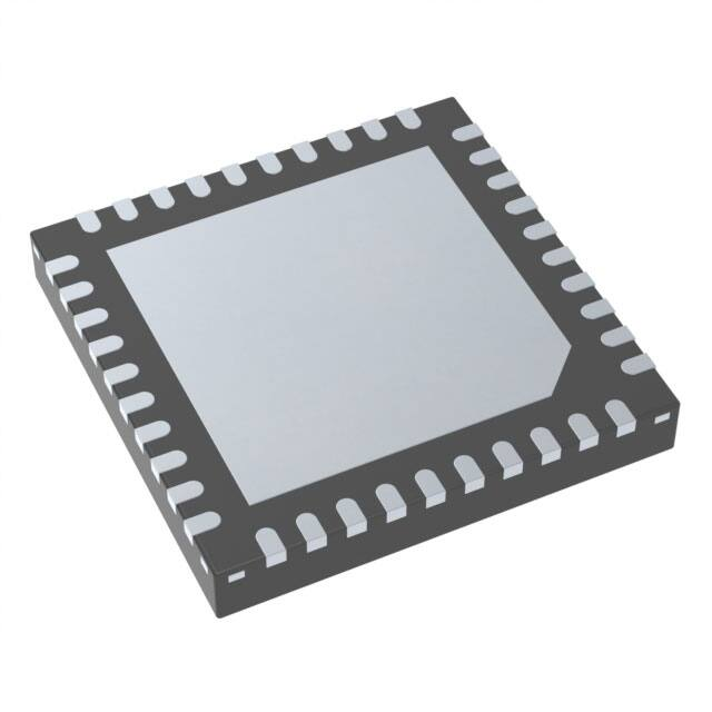


 工商网监
湘ICP备2023018690号
工商网监
湘ICP备2023018690号
