Features
Datasheet
RX64M Group
R01DS0173EJ0120
Rev.1.20
Oct 20, 2022
Renesas MCUs
120-MHz 32-bit RX MCU, on-chip FPU, 240 DMIPS, up to 4-MB flash memory,
512-KB SRAM, various communications interfaces including IEEE 1588-compliant Ethernet MAC,
full-speed USB 2.0 with battery charging, SD host interface (optional), quad SPI, and CAN, 12-bit A/D
converter, RTC, encryption (optional), serial interface for audio, CMOS camera interface
Features
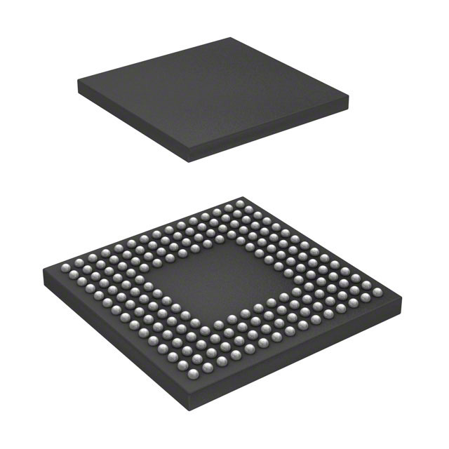
PLQP0176KB-A 24 × 24 mm, 0.5-mm pitch
PLQP0144KA-A 20 × 20 mm, 0.5-mm pitch
PLQP0100KB-A 14 × 14 mm, 0.5-mm pitch
■ 32-bit RXv2 CPU core
Max. operating frequency: 120 MHz
Capable of 240 DMIPS in operation at 120 MHz
Single precision 32-bit IEEE-754 floating point
Two types of multiply-and-accumulation unit (between memories
and between registers)
32-bit multiplier (fastest instruction execution takes one CPU clock
cycle)
Divider (fastest instruction execution takes two CPU clock cycles)
Fast interrupt
CISC Harvard architecture with 5-stage pipeline
Variable-length instructions: Ultra-compact code
Supports the memory protection unit (MPU)
JTAG and FINE (one-line) debugging interfaces
■ Low-power design and architecture
Single voltage supply: 2.7 to 3.6 V
Low power consumption: A product that supports all peripheral
functions draws only 0.3mA/MHz (Typ.).
RTC is capable of operation from a dedicated power supply.
Four low-power modes
■ On-chip code flash memory, no wait states
Up to 4 Mbyte
120-MHz operation, 8.3-ns read cycle (no wait states)
User code is programmable by on-board or off-board programming.
Background programming/erasing (BGO:Background operation)
■ On-chip data flash memory
64 Kbytes, reprogrammable up to 100,000 times
Background programming/erasing (BGO:Background operation)
■ On-chip SRAM
512 Kbytes of SRAM (no wait states)
32 Kbytes of RAM with ECC (one wait state, single-error correction
and double error detection)
8 Kbytes of standby RAM (backup on deep software standby)
■ Data transfer
DMAC: 8 channels
DTC
EXDMAC: 2 channels
DMAC for the Ethernet controller: 3 channels for 176- and 177-pin
products; 2 channels for 100-, 144-, and 145-pin products
■ Reset and supply management
Power-on reset (POR)
Low voltage detection (LVD) with voltage settings
■ Clock functions
External crystal resonator or internal PLL for operation at 8 to 24
MHz
Internal 240-kHz LOCO and HOCO selectable from 16, 18, and 20
MHz
120-kHz clock for the IWDTa
■ Real-time clock
Adjustment functions (30 seconds, leap year, and error)
Real-time clock counting and binary counting modes are selectable
Time capture function
(for capturing times in response to event-signal input)
■ Independent watchdog timer
120-kHz (1/2 LOCO frequency) clock operation
■ Useful functions for IEC60730 compliance
Oscillation-stoppage detection, frequency measurement, CRC,
IWDTa, self-diagnostic function for the A/D converter, etc.
Register write protection function can protect values in important
registers against overwriting.
R01DS0173EJ0120 Rev.1.20
Oct 20, 2022
PTLG0177KA-A 8 × 8 mm, 0.5-mm pitch
PTLG0145KA-A 7 × 7 mm, 0.5-mm pitch
PTLG0100JA-A 7 × 7 mm, 0.65-mm pitch
PLBG0176GA-A 13 × 13mm, 0.8-mm pitch
■ Various communications interfaces
IEEE 1588-compliant Ethernet MAC
(for 176- and 177-pin products: 2 modules)
PHY layer for host/function or OTG controller (1) with full-speed
USB 2.0 with battery charging transfer (only for 176- and 177-pin
products)
PHY layer (1) for host/function or OTG controller (1) with fullspeed USB 2.0 transfer
CAN (compliant with ISO11898-1), incorporating 32 mailboxes (up
to 3 modules)
SCIg and SCIh with multiple functionalities (up to 9)
Choose from among asynchronous mode, clock-synchronous mode,
smart-card interface mode, simplified SPI, simplified I2C, and
extended serial mode.
SCIFA with 16-byte transmission and reception FIFOs (up to 4
interfaces)
I2C bus interface for transfer at up to 1 Mbps (up to 2 interfaces)
Four-wire QSPI (1 interface) in addition to RSPIa (1 interface)
Parallel data capture unit (PDC) for the CMOS camera interface (not
in 100-pin products)
SD host interface (optional: 1 interface) with a 1- or 4-bit SD bus for
use with SD memory or SDIO
■ External address space
Buses for full-speed data transfer (max. operating frequency of 60
MHz)
8 CS areas
8-, 16-, or 32-bit bus space is selectable per area
Independent SDRAM area (128 Mbytes)
■ Up to 29 extended-function timers
16-bit TPUa, MTU3a, and GPTA: input capture, output compare,
PWM waveform output
8-bit TMRa (4 channels), 16-bit CMT (4 channels), 32-bit CMTW (2
channels)
■ 12-bit A/D converter
Two 12-bit units (8 channels for unit 0; 21 channels for unit 1)
Self diagnosis
Detection of analog input disconnection
■ 12-bit D/A converter: 2 channels
On-chip operational amplifier output or direct input selectable
■ Temperature sensor for measuring temperature
within the chip
■ Encryption (optional)
AES (key lengths: 128, 192, and 256 bits)
DES (key lengths: 56 bits (DES); 3 × 56 bits (T-DES))
SHA (SHA-1 (128), SHA-2 (224 or 256), HMAC (160, 224, or 256))
■ Up to 127 pins for general I/O ports
5-V tolerance, open drain, input pull-up, switchable driving ability
■ Operating temp. range
D-version: –40C to +85C
G-version: –40C to +105C
Page 1 of 162
�RX64M Group
1. Overview
1.
Overview
1.1
Outline of Specifications
Table 1.1 lists the specifications in outline, and Table 1.2 gives a comparison of the functions of products in different
packages.
Table 1.1 shows the outline of maximum specifications, and the number of peripheral module channels differs
depending on the pin number on the package and the code flash memory capacity. For details, see Table 1.2,
Comparison of Functions for Different Packages.
Table 1.1
Outline of Specifications (1/9)
Classification
Module/Function
Description
CPU
CPU
Maximum operating frequency: 120 MHz
32-bit RX CPU (RXv2)
Minimum instruction execution time: One instruction per state (cycle of the system
clock)
Address space: 4-Gbyte linear
Register set of the CPU
General purpose: Sixteen 32-bit registers
Control: Ten 32-bit registers
Accumulator: Two 72-bit registers
Basic instructions: 75
Floating-point instructions: 11
DSP instructions: 23
Addressing modes: 11
Data arrangement
Instructions: Little endian
Data: Selectable as little endian or big endian
On-chip 32-bit multiplier: 32 × 32 → 64 bits
On-chip divider: 32 / 32 → 32 bits
Barrel shifter: 32 bits
FPU
Single precision (32-bit) floating point
Data types and floating-point exceptions in conformance with the IEEE754 standard
Code flash memory
Data flash memory
Capacity: 64 Kbytes
Programming/erasing: 100,000 times
RAM
Capacity: 512 Kbytes
120 MHz, no-wait access
SED (single error detection)
Unique ID
12-byte length ID unique to the device
RAM with ECC
Capacity: 32 Kbytes
120 MHz, single wait access
SEC-DED (single error correction/double error detection)
Standby RAM
Capacity: 8 Kbytes
Operation synchronized with PCLKB: Up to 60 MHz, two-cycle access
Memory
Operating modes
R01DS0173EJ0120 Rev.1.20
Oct 20, 2022
Capacity: 2 Mbytes, 2.5 Mbytes, 3 Mbytes, 4 Mbytes
120 MHz, no-wait access
On-board programming: Four types
Off-board programming (parallel programmer mode)
The trusted memory (TM) function protects against the reading of programs from blocks
8 and 9.
Operating modes by the mode-setting pins at the time of release from the reset state
Single-chip mode
Boot mode (for the SCI interface)
Boot mode (for the USB interface)
User boot mode
Selection of operating mode by register setting
Single-chip mode, user boot mode
On-chip ROM disabled extended mode
On-chip ROM enabled extended mode
Endian selectable
Page 2 of 162
�RX64M Group
Table 1.1
1. Overview
Outline of Specifications (2/9)
Classification
Module/Function
Description
Clock
Clock generation circuit
Main clock oscillator, sub clock oscillator, low-speed/high-speed on-chip oscillator, PLL
frequency synthesizer, and IWDT-dedicated on-chip oscillator
The peripheral module clocks can be set to frequencies above that of the system clock.
Main-clock oscillation stoppage detection
Separate frequency-division and multiplication settings for the system clock (ICLK),
peripheral module clocks (PCLKA, PCLKB, PCLKC, PCLKD), flash-IF clock (FCLK) and
external bus clock (BCLK)
The CPU and other bus masters run in synchronization with the system clock (ICLK):
Up to 120 MHz
Peripheral modules of MTU3, GPT, RSPI, SCIFA, USBA, ETHERC, EPTPC, EDMAC,
and AES run in synchronization with PCLKA, which operates at up to 120 MHz.
Other peripheral modules run in synchronization with PCLKB: Up to 60 MHz
ADCLK in the S12AD (unit 0) runs in synchronization with PCLKC: Up to 60 MHz
ADCLK in the S12AD (unit 1) runs in synchronization with PCLKD: Up to 60 MHz
Flash IF run in synchronization with the flash-IF clock (FCLK): Up to 60 MHz
Devices connected to the external bus run in synchronization with the external bus
clock (BCLK): Up to 60 MHz
Multiplication is possible with using the high-speed on-chip oscillator (HOCO) as a
reference clock of the PLL circuit
Reset
Nine types of reset
RES# pin reset: Generated when the RES# pin is driven low.
Power-on reset: Generated when the RES# pin is driven high and VCC = AVCC0 =
AVCC1 rises.
Voltage-monitoring 0 reset: Generated when VCC = AVCC0 = AVCC1 falls.
Voltage-monitoring 1 reset: Generated when VCC = AVCC0 = AVCC1 falls.
Voltage-monitoring 2 reset: Generated when VCC = AVCC0 = AVCC1 falls.
Deep software standby reset: Generated in response to an interrupt to trigger release
from deep software standby.
Independent watchdog timer reset: Generated when the independent watchdog timer
underflows, or a refresh error occurs.
Watchdog timer reset: Generated when the watchdog timer underflows, or a refresh
error occurs.
Software reset: Generated by register setting.
Power-on reset
If the RES# pin is at the high level when power is supplied, an internal reset is generated.
After VCC = AVCC0 = AVCC1 has exceeded the voltage detection level and the specified
period has elapsed, the reset is cancelled.
Voltage detection circuit (LVDA)
Monitors the voltage being input to the VCC = AVCC0 = AVCC1 pins and generates an
internal reset or internal interrupt.
Voltage detection circuit 0
Capable of generating an internal reset
The option-setting memory can be used to select enabling or disabling of the reset.
Voltage detection level: Selectable from three different levels (2.94 V, 2.87 V, and
2.80 V)
Voltage detection circuits 1 and 2
Voltage detection level: Selectable from three different levels (2.99 V, 2.92 V, and
2.85 V)
Digital filtering (1/2, 1/4, 1/8, and 1/16 LOCO frequency)
Capable of generating an internal reset
Two types of timing are selectable for release from reset
An internal interrupt can be requested.
Detection of voltage rising above and falling below thresholds is selectable.
Maskable or non-maskable interrupt is selectable
Voltage detection monitoring
Event linking
Low power
consumption
Low power
consumption facilities
Module stop function
Four low power consumption modes
Sleep mode, all-module clock stop mode, software standby mode, and deep software
standby mode
Battery backup function
When the voltage on the VCC pin drops, battery power from the VBATT pin is supplied
to keep the real-time clock (RTC) operating.
R01DS0173EJ0120 Rev.1.20
Oct 20, 2022
Page 3 of 162
�RX64M Group
Table 1.1
1. Overview
Outline of Specifications (3/9)
Classification
Module/Function
Description
Interrupt
Interrupt controller
(ICUA)
Peripheral function interrupts: 293 sources
External interrupts: 16 (pins IRQ0 to IRQ15)
Software interrupts: 2 sources
Non-maskable interrupts: 7 sources
Sixteen levels specifiable for the order of priority
Method of interrupt source selection:
The interrupt vectors consist of 256 vectors (128 sources are fixed. The remaining 128
vectors are selected from among the other 156 sources.)
External bus extension
The external address space can be divided into eight areas (CS0 to CS7), each with
independent control of access settings.
Capacity of each area: 16 Mbytes (CS0 to CS7)
A chip-select signal (CS0# to CS7#) can be output for each area.
Each area is specifiable as an 8-, 16-, or 32-bit bus space.
The data arrangement in each area is selectable as little or big endian (only for data).
SDRAM interface connectable
Bus format: Separate bus, multiplex bus
Wait control
Write buffer facility
DMA
DMA controller
(DMACAa)
8 channels
Three transfer modes: Normal transfer, repeat transfer, and block transfer
Request sources: Software trigger, external interrupts, and interrupt requests from
peripheral functions
EXDMA controller
(EXDMACa)
2 channels
Four transfer modes: Normal transfer, repeat transfer, block transfer, and cluster
transfer
Single-address transfer enabled with the EDACKn signal
Request sources: Software trigger, external DMA requests (EDREQn), and interrupt
requests from peripheral functions
Data transfer controller
(DTCa)
Three transfer modes: Normal transfer, repeat transfer, and block transfer
Request sources: External interrupts and interrupt requests from peripheral functions
Programmable I/O ports
I/O ports for the 177-pin TFLGA, 176-pin LFBGA, and 176-pin LFQFP
I/O pins: 127
Input pin: 1
Pull-up resistors: 127
Open-drain outputs: 127
5-V tolerance: 19
I/O ports for the 145-pin TFLGA and 144-pin LFQFP
I/O pins: 111
Input pin: 1
Pull-up resistors: 111
Open-drain outputs: 111
5-V tolerance: 18
I/O ports for the 100-pin TFLGA and 100-pin LFQFP
I/O pins: 78
Input pin: 1
Pull-up resistors: 78
Open-drain outputs: 78
5-V tolerance: 17
I/O ports
Event link controller (ELC)
R01DS0173EJ0120 Rev.1.20
Oct 20, 2022
Event signals such as interrupt request signals can be interlinked with the operation of
functions such as timer counting, eliminating the need for intervention by the CPU to
control the functions.
119 internal event signals can be freely combined for interlinked operation with
connected functions.
Event signals from peripheral modules can be used to change the states of output pins
(of ports B and E).
Changes in the states of pins (of ports B and E) being used as inputs can be interlinked
with the operation of peripheral modules.
Page 4 of 162
�RX64M Group
Table 1.1
1. Overview
Outline of Specifications (4/9)
Classification
Module/Function
Description
Timers
16-bit timer pulse unit
(TPUa)
(16 bits × 6 channels) × 1 unit
Maximum of 16 pulse-input/output possible
Select from among seven or eight counter-input clock signals for each channel
Input capture/output compare function
Output of PWM waveforms in up to 15 phases in PWM mode
Support for buffered operation, phase-counting mode (two phase encoder input) and
cascade-connected operation (32 bits × 2 channels) depending on the channel.
PPG output trigger can be generated
Capable of generating conversion start triggers for the A/D converters
Digital filtering of signals from the input capture pins
Event linking by the ELC
Multifunction timer
pulse unit (MTU3a)
9 channels (16 bits × 8 channels, 32 bits × 1 channel)
Maximum of 28 pulse-input/output and 3 pulse-input possible
Select from among 14 counter-input clock signals for each channel (PCLKA/1, PCLKA/
2, PCLKA/4, PCLKA/8, PCLKA/16, PCLKA/32, PCLKA/64, PCLKA/256, PCLKA/1024,
MTCLKA, MTCLKB, MTCLKC, MTCLKD, MTIOC1A)
14 of the signals are available for channel 0, 12 are available for channel 2, 11 are
available for channels 1, 3, 4, 6 to 8, and 10 are available for channel 5.
Input capture function
39 output compare/input capture registers
Counter clear operation (synchronous clearing by compare match/input capture)
Simultaneous writing to multiple timer counters (TCNT)
Simultaneous register input/output by synchronous counter operation
Buffered operation
Support for cascade-connected operation
43 interrupt sources
Automatic transfer of register data
Pulse output mode
Toggle/PWM/complementary PWM/reset-synchronized PWM
Complementary PWM output mode
Outputs non-overlapping waveforms for controlling 3-phase inverters
Automatic specification of dead times
PWM duty cycle: Selectable as any value from 0% to 100%
Delay can be applied to requests for A/D conversion.
Non-generation of interrupt requests at peak or trough values of counters can be
selected.
Double buffer configuration
Reset synchronous PWM mode
Three phases of positive and negative PWM waveforms can be output with desired duty
cycles.
Phase-counting mode: 16-bit mode (channels 1 and 2); 32-bit mode (channels 1 and 2)
Counter functionality for dead-time compensation
Generation of triggers for A/D converter conversion
A/D converter start triggers can be skipped
Digital filter function for signals on the input capture and external counter clock pins
PPG output trigger can be generated
Event linking by the ELC
Port output enable 3
(POE3a)
Control of the high-impedance state of the MTU3/GPT's waveform output pins
5 pins for input from signal sources: POE0, POE4, POE8, POE10, POE11
Initiation on detection of short-circuited outputs (detection of simultaneous PWM output
to the active level)
Initiation by oscillation-stoppage detection or software
The conditions for control can be set for the target pins subject to output control.
R01DS0173EJ0120 Rev.1.20
Oct 20, 2022
Page 5 of 162
�RX64M Group
Table 1.1
1. Overview
Outline of Specifications (5/9)
Classification
Module/Function
Description
Timers
General PWM timer
(GPTA)
16 bits × 4 channels
Counting up or down (saw-wave), counting up and down (triangle-wave) selectable for
all channels
Four clock sources independently selectable for all channels (PCLKA/1, PCLKA/4,
PCLKA/8, PCLKA/16)
2 input/output pins per channel
2 output compare/input capture registers per channel
For the 2 output compare/input capture registers of each channel, 4 registers are
provided as buffer registers and are capable of operating as comparison registers when
buffering is not in use.
In output compare operation, buffer switching can be at peaks or troughs, enabling the
generation of laterally asymmetrically PWM waveforms.
Registers for setting up frame intervals on each channel (with capability for generating
interrupts on overflow or underflow)
Synchronizable operation of the several counters
Modes of synchronized operation (synchronized, or displaced by desired times for
phase shifting)
Generation of dead times in PWM operation
Through combination of three counters, generation of automatic three-phase PWM
waveforms incorporating dead times
Starting, clearing, and stopping counters in response to external or internal triggers
Internal trigger sources: output of the internal comparator detection, software, and
compare-match
Digital filter function for signals on the input capture and external trigger pins
Event linking by the ELC
Programmable pulse
generator (PPG)
(4 bits × 4 groups) × 2 units
Pulse output with the MTU or TPU output as a trigger
Maximum of 32 pulse-output possible
8-bit timers (TMRb)
(8 bits × 2 channels) × 2 units
Select from among seven internal clock signals (PCLKB/1, PCLKB/2, PCLKB/8,
PCLKB/32, PCLKB/64, PCLKB/1024, PCLKB/8192) and one external clock signal
Capable of output of pulse trains with desired duty cycles or of PWM signals
The 2 channels of each unit can be cascaded to create a 16-bit timer
Generation of triggers for A/D converter conversion
Capable of generating the internal operating clock signals for SCI5, SCI6, or SCI12
Event linking by the ELC
Compare match timer
(CMT)
(16 bits × 2 channels) × 2 units
Select from among four internal clock signals (PCLKB/8, PCLKB/32, PCLKB/128,
PCLKB/512)
Event linking by the ELC
Compare match timer
W (CMTW)
(32 bits × 1 channel) × 2 units
Compare-match, input-capture input, and output-comparison output are available.
Select from among four internal clock signals (PCLKB/8, PCLKB/32, PCLKB/128,
PCLKB/512)
Interrupt requests can be output in response to compare-match, input-capture, and
output-comparison events.
Event linking by the ELC
Realtime clock (RTCd)
Clock sources: Main clock, sub clock
Selection of the 32-bit binary count in time count/second unit possible
Clock and calendar functions
Interrupt sources: Alarm interrupt, periodic interrupt, and carry interrupt
Battery backup operation
Time-capture facility for three values
Event linking by the ELC
Watchdog timer (WDTA) 14 bits × 1 channel
Select from among 6 counter-input clock signals (PCLKB/4, PCLKB/64, PCLKB/128,
PCLKB/512, PCLKB/2048, PCLKB/8192)
R01DS0173EJ0120 Rev.1.20
Oct 20, 2022
Page 6 of 162
�RX64M Group
Table 1.1
1. Overview
Outline of Specifications (6/9)
Classification
Module/Function
Description
Timers
Independent watchdog
timer (IWDTa)
14 bits × 1 channel
Counter-input clock: IWDT-dedicated on-chip oscillator
Dedicated clock/1, dedicated clock/16, dedicated clock/32, dedicated clock/64,
dedicated clock/128, dedicated clock/256
Window function: The positions where the window starts and ends are specifiable (the
window defines the timing with which refreshing is enabled and disabled).
Event linking by the ELC
Communication
function
Ethernet controller
(ETHERC)
2 channels
Input and output of Ethernet/IEEE 802.3 frames
Transfer at 10 or 100 Mbps
Full- and half-duplex modes
MII (Media Independent Interface) or RMII (Reduced Media Independent Interface) as
defined in IEEE 802.3u
Detection of Magic PacketsTM*1 or output of a “wake-on-LAN” signal (WOL)
Compliance with flow control as defined in IEEE 802.3x standards
Filtering of multicast frames
Direct transfer of frames between two channels by cut-through
PTP controller for
Ethernet controller
(EPTPC)
A block compatible with the IEEE 1588 standard is connected to the Ethernet controller
(ETHERC).
Matching with a time stamp can start counting by MTU3 and the GPT.
DMA controller for
Ethernet controller
(EDMACa)
3 channels (the round-robin method determines the priority of the channels)
2 channels for ETHERC; 1 channel for EPTPC
Alleviation of CPU load by the descriptor control method
Transmission FIFO: 2 Kbytes; Reception FIFO: 4 Kbytes
USB 2.0 FS host/
function module (USBb)
Includes a UDC (USB Device Controller) and transceiver for USB 2.0 FS
One port
Compliance with the USB 2.0 specification
Transfer rate: Full speed (12 Mbps), low speed (1.5 Mbps) (host only)
Both self-power mode and bus power are supported
OTG (On the Go) operation is possible (low-speed is not supported)
Incorporates 2 Kbytes of RAM as a transfer buffer
External pull-up and pull-down resistors are not required
USB 2.0 FS host/
function module with
battery charging
(USBA)
Includes a UDC (USB Device Controller) and transceiver for USB 2.0 FS
One port (only in 176-pin devices)
Compliance with the USB 2.0 specification
Transfer rate: Full speed (12 Mbps),
low speed (1.5 Mbps) (host only)
Both self-power mode and bus power are supported
OTG (On the Go) operation is possible (low-speed is not supported)
Incorporates 8.5 Kbytes of RAM as a transfer buffer
External pull-up and pull-down resistors are not required
Serial communications
interfaces (SCIg, SCIh)
R01DS0173EJ0120 Rev.1.20
Oct 20, 2022
9 channels (SCIg: 8 channels + SCIh: 1 channel)
SCIg
Serial communications modes: Asynchronous, clock synchronous, and smart-card
interface
Multi-processor function
On-chip baud rate generator allows selection of the desired bit rate
Choice of LSB-first or MSB-first transfer
Average transfer rate clock can be input from TMR timers for SCI5, SCI6, and SCI12
Start-bit detection: Level or edge detection is selectable.
Simple I2C
Simple SPI
9-bit transfer mode
Bit rate modulation
Double-speed mode
Event linking by the ELC (supported by SCI5 only)
SCIh (The following functions are added to SCIg)
Supports the serial communications protocol, which contains the start frame and
information frame
Supports the LIN format
Page 7 of 162
�RX64M Group
Table 1.1
1. Overview
Outline of Specifications (7/9)
Classification
Module/Function
Description
Communication
function
Serial communications
interface with FIFO
(SCIFA)
I2C bus interface
(RIICa)
2 channels (only channel 0 can be used in fast-mode plus)
Communication formats
I2C bus format/SMBus format
Supports the multi-master
Max. transfer rate: 1 Mbps (channel 0)
Event linking by the ELC
CAN module (CAN)
3 channels
Compliance with the ISO11898-1 specification (standard frame and extended frame)
32 mailboxes per channel
Serial peripheral
interface (RSPIa)
1 channel
RSPI transfer facility
Using the MOSI (master out, slave in), MISO (master in, slave out), SSL (slave select),
and RSPCK (RSPI clock) signals enables serial transfer through SPI operation (four
lines) or clock-synchronous operation (three lines)
Capable of handling serial transfer as a master or slave
Data formats
Switching between MSB first and LSB first
The number of bits in each transfer can be changed to any number of bits from 8 to 16,
or to 20, 24, or 32 bits.
128-bit buffers for transmission and reception
Up to four frames can be transmitted or received in a single transfer operation (with
each frame having up to 32 bits)
Buffered structure
Double buffers for both transmission and reception
RSPCK can be stopped with the receive buffer full for master reception.
Event linking by the ELC
Quad serial peripheral
interface (QSPI)
1 channel
Connectable with serial flash memory equipped with multiple input and output lines (i.e.
for single, dual, or quad operation)
Selectable bit length, polarity, and phase of the clock signal
Sequential execution of transfer
LSB or MSB first is selectable.
4 channels
Methods of transfer: Asynchronous and clock synchronous
Desired bit rates can be selected from the internal baud rate generators.
LSB or MSB first is selectable.
Both the transmission and reception sections are equipped with 16-byte FIFO buffers,
allowing continuous transmission and reception.
Bit rate modulation
Double-speed mode
Serial sound interface (SSI)
2 channels
Full-duplex transfer is possible (only on channel 0).
Support for multiple audio formats
Support for master or slave operation
Bit clock frequency is selectable from four different types (16 fs, 32 fs, 48 fs, and 64 fs).
Support for 8-/16-/18-/20-/22-/24 bit data formats
Internal 8-stage FIFO for transmission and reception
Stopping SSIWS when data transfer is stopped is selectable.
Sampling rate converter (SRC)
1 channel
Data formats: 32-bit stereo (16 bits for the left, 16 bits for the right) and 16-bit monaural.
Input sampling rates: 8, 11.025, 12, 16, 22.05, 24, 32, 44.1, 48 kHz
Output sampling rates: 32, 44.1, 48, 8*2 or 16 kHz*2
SD host interface (SDHI)*4
1 channel
Transfer speed: Supports high-speed mode (15 MB/s) and default speed mode (10 MB/s)
One interface for SD memory and I/O cards (supporting 1- and 4-bit SD buses)
SD specifications
Part 1: Physical Layer Specification Ver. 3.01 compliant (DDR not supported)
Part E1: SDIO Specification Ver. 3.00
Error checking: CRC7 for commands and CRC16 for data
Interrupt requests: Card access interrupt, SDIO access interrupt, card detection
interrupt
DMA transfer requests: SD_BUF write and SD_BUF read
Support for card detection and write protection
R01DS0173EJ0120 Rev.1.20
Oct 20, 2022
Page 8 of 162
�RX64M Group
Table 1.1
Classification
1. Overview
Outline of Specifications (8/9)
Module/Function
Description
MMC host interface (MMCIF)
1 channel
Transfer speed: Supports high-speed mode (30 MB/s) and Backward-compatible mode
(25 MB/s)
Compliant with JEDEC STANDARD JESD84-A441 (DDR is not supported)
Interface for Multimedia Cards (MMCs)
Device buses: Support for 1-, 4-, and 8-bit MMC buses
Interrupt requests: Card detection interrupt, error/timeout interrupt, normal operation
interrupt
DMA transfer requests: CE_DATA write and CE_DATA read
Support for card detection, boot operation, high priority interrupt (HPI)
Parallel data capture unit (PDC)
1 channel
Acquisition of synchronization through external 8-bit horizontal and vertical
synchronization signals
Setting of the image size when clipping of the output for a one-frame image is required
12-bit A/D converter (S12ADC)
12 bits × 2 units (unit 0: 8 channels; unit 1: 21 channels)
12-bit resolution (switchable between 8, 10, and 12 bits)
Conversion time
0.48 µs per channel (for 12-bit conversion)
0.45 µs per channel (for 10-bit conversion)
0.42 µs per channel (for 8-bit conversion)
Operating mode
Scan mode (single scan mode, continuous scan mode, or group scan mode)
Group A priority control (only for group scan mode)
Sample-and-hold function
Common sample-and-hold circuit included
In addition, channel-dedicated sample-and-hold function (3ch: in unit 0 only) included
Sampling variable
Sampling time can be set up for each channel.
Digital comparison
Method: Comparison to detect voltages above or below thresholds and window
comparison
Measurement: Comparison of two results of conversion or comparison of a value in the
comparison register and a result of conversion
Self-diagnostic function
The self-diagnostic function internally generates three analog input voltages (unit 0:
VREFL0, VREFH0 × 1/2, VREFH0; unit 1: AVSS1, AVCC1 × 1/2, AVCC1)
Double trigger mode (A/D conversion data duplicated)
Detection of analog input disconnection
Three ways to start A/D conversion
Software trigger, timer (MTU3, GPT, TMR, TPU) trigger, external trigger
Event linking by the ELC
12-bit D/A converter (R12DA)
Temperature sensor
1 channel
Relative precision: ±1°C
The voltage of the temperature is converted into a digital value by the 12-bit A/D
converter (unit 1).
Safety
Memory protection unit
(MPU)
Protection area: Eight areas (max.) can be specified in the range from 0000 0000h to
FFFF FFFFh.
Minimum protection unit: 16 bytes
Reading from, writing to, and enabling the execution access can be specified for each
area.
An address exception occurs when the detected access is not in the permitted area.
Trusted Memory (TM)
Function
Protects against the reading of programs from blocks 8 and 9 of the code flash memory
Instruction fetching by the CPU is the only form of access to these areas when the TM
function is enabled.
Register write
protection function
Protects important registers from being overwritten for in case a program runs out of
control.
R01DS0173EJ0120 Rev.1.20
Oct 20, 2022
2 channels
12-bit resolution
Output voltage: 0.2 V to AVCC1 – 0.2 V (amplifier output), 0 V to AVCC1 (direct output)
Output via an amplifier or direct output can be selected.
Event linking by the ELC
Page 9 of 162
�RX64M Group
Table 1.1
1. Overview
Outline of Specifications (9/9)
Classification
Module/Function
Description
Safety
CRC calculator (CRC)
CRC code generation for arbitrary amounts of data in 8-bit units
Select any of three generating polynomials:
X8 + X2 + X + 1, X16 + X15 + X2 + 1, or X16 + X12 + X5 + 1
Generation of CRC codes for use with LSB-first or MSB-first communications is
selectable
Oscillation stop
detection function for
the main clock
Main clock oscillation stop detection: Available
Clock frequency
accuracy measurement
circuit (CAC)
Monitors the clock output from the main clock oscillator, sub-clock oscillator, low- and
high-speed on-chip oscillators, the PLL frequency synthesizer, IWDT-dedicated on-chip
oscillator, and PCLKB, and generates interrupts when the setting range is exceeded.
Data operation circuit
(DOC)
The function to compare, add, or subtract 16-bit data
AES*3
Key lengths: 128, 192, and 256 bits
Support for CBC, ECB, CFB, OFB, CTR, and CMAC operating modes
Speed of calculations: 128-bit key length in 22 cycles
192-bit key length in 26 cycles
256-bit key length in 30 cycles
Compliant with FIPS PUB 197
DES*3
Key lengths: 56 bits (DES)/3 × 56 bits (T-DES)
Support for DES and triple DES
Support for ECB and CBC operating modes
Speed of calculations: 6 clock cycles in single DES mode
14 clock cycles in triple DES mode
Compliant with FIPS PUB 46-3
Compliant with FIPS PUB 81
SHA*3
Support for SHA-1 (128), SHA-2 (224 or 256), and HMAC (160, 224, or 256)
Speed of calculations: 50 clock cycles in SHA-1 mode
42 clock cycles in SHA-224 mode
42 clock cycles in SHA-256 mode
Compliant with SHA as defined in FIPS PUB 180-1 and -2
Compliant with HMAC as defined in FIPS PUB 198
True random number
generator (RNG)*3
Length of random numbers: 16 bits
Generation of random-number-generated interrupts after a number is generated
Random number generation time: 3.6 ms (typ)
Encryption
function
Operating frequency
Up to 120 MHz
Power supply voltage
VCC = AVCC0 = AVCC1 = VCC_USB = 2.7 to 3.6 V, 2.7 VREFH0 AVCC0,
VCC_USBA = AVCC_USBA = 2.7 to 3.6 V,
VBATT = 2.0 to 3.6 V
Operating temperature
D-version: –40 to +85°C
G-version: –40 to +105°C*5
Package
177-pin TFLGA (PTLG0177KA-A)
176-pin LFBGA (PLBG0176GA-A)
176-pin LFQFP (PLQP0176KB-A)
145-pin TFLGA (PTLG0145KA-A)
144-pin LFQFP (PLQP0144KA-A)
100-pin TFLGA (PTLG0100JA-A)
100-pin LFQFP (PLQP0100KB-A)
On-chip debugging system
E1 emulator (JTAG and FINE interfaces)
E20 emulator (JTAG interface)
Note 1.
Note 2.
Note 3.
Note 4.
Note 5.
Magic PacketTM is a registered trademark of Advanced Micro Devices, Inc.
Setting is only possible when the input sampling rate 44.1 kHz is selected.
The product part number differs according to whether or not it supports encryption.
The product part number differs according to whether or not it includes an SDHI (SD host interface).
Please contact us if you are using a G-version product.
R01DS0173EJ0120 Rev.1.20
Oct 20, 2022
Page 10 of 162
�RX64M Group
Table 1.2
1. Overview
Comparison of Functions for Different Packages (1/2)
Functions
RX64M Group
Package
External bus
177 Pins, 176 Pins
External bus width
32 bits
Available
Not supported
DMA controller
Ch. 0 to 7
Data transfer controller
Available
EXDMA controller
Timers
Ch. 0 and 1
16-bit timer pulse unit
Ch. 0 to 5
Multi-function timer pulse unit 3
Ch. 0 to 8
General-purpose PWM timer
Ch. 0 to 3
Port output enable 3
Available
Programmable pulse generator
Ch. 0 and 1
8-bit timers
Ch. 0 to 3
Compare match timer
Ch. 0 to 3
Compare match timer W
Communication
function
Ch. 0 and 1
Realtime clock
Available
Watchdog timer
Available
Independent watchdog timer
Available
Ethernet controller
Ch. 0 and 1
Ch. 0
PTP controller for ethernet controller
DMAC controller for ethernet
Available
Ch. 0 and 1 (ETHERC)
Ch. 2 (EPTPC)
Ch. 0 (ETHERC) and 2 (EPTPC)
USB 2.0 FS host/function module
USB 2.0 FS host/function module with battery
charging
Serial communications interfaces (SCIg)
Ch. 0
Available
Not supported
Ch. 0 to 7
Ch. 0 to 3, 5 and 6
Serial communications interfaces (SCIh)
Serial communications interfaces with FIFO
Ch. 12
Ch. 8 to 11
I2C bus interfaces
Ch. 8 and 9
Ch. 0 and 2
Serial peripheral interface
CAN module
Ch. 0
Ch. 0 to 2
Ch. 0 and 1
Quad serial peripheral interface
Ch. 0
Serial sound interfaces
Ch. 0 and 1
Sampling rate converter
Available
SD host interface
Ch. 0
MMC host interface
Parallel data capture unit
100 Pins
16 bits
SDRAM area controller
DMA
145 Pins, 144 Pins
Ch. 0
Available
Not supported
12-bit A/D converter
AN000 to 007 (unit 0: 8 channels)
AN100 to 120 (unit 1: 21 channels)
AN000 to 007
(unit 0: 8 channels)
AN100 to 113
(unit 1: 14
channels)
12-bit D/A converter
Ch. 0 and 1
Ch. 1
Temperature sensor
Available
CRC calculator
Available
Data operation circuit
Available
Clock frequency accuracy measurement circuit
Available
AES
Available
R01DS0173EJ0120 Rev.1.20
Oct 20, 2022
Page 11 of 162
�RX64M Group
Table 1.2
1. Overview
Comparison of Functions for Different Packages (2/2)
Functions
Package
RX64M Group
177 Pins, 176 Pins
145 Pins, 144 Pins
DES
Available
SHA
Available
RNG
Available
Event link controller
Available
R01DS0173EJ0120 Rev.1.20
Oct 20, 2022
100 Pins
Page 12 of 162
�RX64M Group
1.2
1. Overview
List of Products
Table 1.3 is a list of products, and Figure 1.1 shows how to read the product part no.
Table 1.3
List of Products (1/4)
Group
Part No.
Package
Code Flash
Memory
Capacity
RX64M
(Dversion)
R5F564MLCDFC
PLQP0176KB-A
4 Mbytes
RAM
Capacity
Data Flash
Memory
Capacity
Operating
Frequency
(Max.)
Encryption
Module
SDHI
512 Kbytes
64 Kbytes
120 MHz
Not supported
Not supported
R5F564MLDDFC
PLQP0176KB-A
4 Mbytes
512 Kbytes
64 Kbytes
120 MHz
Not supported
Available
R5F564MLGDFC
PLQP0176KB-A
4 Mbytes
512 Kbytes
64 Kbytes
120 MHz
Available
Not supported
R5F564MLHDFC
PLQP0176KB-A
4 Mbytes
512 Kbytes
64 Kbytes
120 MHz
Available
Available
R5F564MJCDFC
PLQP0176KB-A
3 Mbytes
512 Kbytes
64 Kbytes
120 MHz
Not supported
Not supported
R5F564MJDDFC
PLQP0176KB-A
3 Mbytes
512 Kbytes
64 Kbytes
120 MHz
Not supported
Available
R5F564MJGDFC
PLQP0176KB-A
3 Mbytes
512 Kbytes
64 Kbytes
120 MHz
Available
Not supported
R5F564MJHDFC
PLQP0176KB-A
3 Mbytes
512 Kbytes
64 Kbytes
120 MHz
Available
Available
R5F564MGCDFC
PLQP0176KB-A
2.5 Mbytes
512 Kbytes
64 Kbytes
120 MHz
Not supported
Not supported
R5F564MGDDFC
PLQP0176KB-A
2.5 Mbytes
512 Kbytes
64 Kbytes
120 MHz
Not supported
Available
R5F564MGGDFC
PLQP0176KB-A
2.5 Mbytes
512 Kbytes
64 Kbytes
120 MHz
Available
Not supported
R5F564MGHDFC
PLQP0176KB-A
2.5 Mbytes
512 Kbytes
64 Kbytes
120 MHz
Available
Available
R5F564MFCDFC
PLQP0176KB-A
2 Mbytes
512 Kbytes
64 Kbytes
120 MHz
Not supported
Not supported
R5F564MFDDFC
PLQP0176KB-A
2 Mbytes
512 Kbytes
64 Kbytes
120 MHz
Not supported
Available
R5F564MFGDFC
PLQP0176KB-A
2 Mbytes
512 Kbytes
64 Kbytes
120 MHz
Available
Not supported
R5F564MFHDFC
PLQP0176KB-A
2 Mbytes
512 Kbytes
64 Kbytes
120 MHz
Available
Available
R5F564MLCDFB
PLQP0144KA-A
4 Mbytes
512 Kbytes
64 Kbytes
120 MHz
Not supported
Not supported
R5F564MLDDFB
PLQP0144KA-A
4 Mbytes
512 Kbytes
64 Kbytes
120 MHz
Not supported
Available
R5F564MLGDFB
PLQP0144KA-A
4 Mbytes
512 Kbytes
64 Kbytes
120 MHz
Available
Not supported
R5F564MLHDFB
PLQP0144KA-A
4 Mbytes
512 Kbytes
64 Kbytes
120 MHz
Available
Available
R5F564MJCDFB
PLQP0144KA-A
3 Mbytes
512 Kbytes
64 Kbytes
120 MHz
Not supported
Not supported
R5F564MJDDFB
PLQP0144KA-A
3 Mbytes
512 Kbytes
64 Kbytes
120 MHz
Not supported
Available
R5F564MJGDFB
PLQP0144KA-A
3 Mbytes
512 Kbytes
64 Kbytes
120 MHz
Available
Not supported
Available
R5F564MJHDFB
PLQP0144KA-A
3 Mbytes
512 Kbytes
64 Kbytes
120 MHz
Available
R5F564MGCDFB
PLQP0144KA-A
2.5 Mbytes
512 Kbytes
64 Kbytes
120 MHz
Not supported
Not supported
R5F564MGDDFB
PLQP0144KA-A
2.5 Mbytes
512 Kbytes
64 Kbytes
120 MHz
Not supported
Available
R5F564MGGDFB
PLQP0144KA-A
2.5 Mbytes
512 Kbytes
64 Kbytes
120 MHz
Available
Not supported
R5F564MGHDFB
PLQP0144KA-A
2.5 Mbytes
512 Kbytes
64 Kbytes
120 MHz
Available
Available
R5F564MFCDFB
PLQP0144KA-A
2 Mbytes
512 Kbytes
64 Kbytes
120 MHz
Not supported
Not supported
R5F564MFDDFB
PLQP0144KA-A
2 Mbytes
512 Kbytes
64 Kbytes
120 MHz
Not supported
Available
R5F564MFGDFB
PLQP0144KA-A
2 Mbytes
512 Kbytes
64 Kbytes
120 MHz
Available
Not supported
R5F564MFHDFB
PLQP0144KA-A
2 Mbytes
512 Kbytes
64 Kbytes
120 MHz
Available
Available
R5F564MLCDFP
PLQP0100KB-A
4 Mbytes
512 Kbytes
64 Kbytes
120 MHz
Not supported
Not supported
R5F564MLDDFP
PLQP0100KB-A
4 Mbytes
512 Kbytes
64 Kbytes
120 MHz
Not supported
Available
R5F564MLGDFP
PLQP0100KB-A
4 Mbytes
512 Kbytes
64 Kbytes
120 MHz
Available
Not supported
R5F564MLHDFP
PLQP0100KB-A
4 Mbytes
512 Kbytes
64 Kbytes
120 MHz
Available
Available
R5F564MJCDFP
PLQP0100KB-A
3 Mbytes
512 Kbytes
64 Kbytes
120 MHz
Not supported
Not supported
R5F564MJDDFP
PLQP0100KB-A
3 Mbytes
512 Kbytes
64 Kbytes
120 MHz
Not supported
Available
R5F564MJGDFP
PLQP0100KB-A
3 Mbytes
512 Kbytes
64 Kbytes
120 MHz
Available
Not supported
R5F564MJHDFP
PLQP0100KB-A
3 Mbytes
512 Kbytes
64 Kbytes
120 MHz
Available
Available
R5F564MGCDFP
PLQP0100KB-A
2.5 Mbytes
512 Kbytes
64 Kbytes
120 MHz
Not supported
Not supported
R5F564MGDDFP
PLQP0100KB-A
2.5 Mbytes
512 Kbytes
64 Kbytes
120 MHz
Not supported
Available
R5F564MGGDFP
PLQP0100KB-A
2.5 Mbytes
512 Kbytes
64 Kbytes
120 MHz
Available
Not supported
R5F564MGHDFP
PLQP0100KB-A
2.5 Mbytes
512 Kbytes
64 Kbytes
120 MHz
Available
Available
R01DS0173EJ0120 Rev.1.20
Oct 20, 2022
Page 13 of 162
�RX64M Group
Table 1.3
1. Overview
List of Products (2/4)
Group
Part No.
Package
Code Flash
Memory
Capacity
RAM
Capacity
Data Flash
Memory
Capacity
Operating
Frequency
(Max.)
Encryption
Module
SDHI
RX64M
(Dversion)
R5F564MFCDFP
PLQP0100KB-A
2 Mbytes
512 Kbytes
64 Kbytes
120 MHz
Not supported
R5F564MFDDFP
PLQP0100KB-A
2 Mbytes
512 Kbytes
64 Kbytes
120 MHz
Not supported
Not supported
Available
R5F564MFGDFP
PLQP0100KB-A
2 Mbytes
512 Kbytes
64 Kbytes
120 MHz
Available
Not supported
R5F564MFHDFP
PLQP0100KB-A
2 Mbytes
512 Kbytes
64 Kbytes
120 MHz
Available
Available
R5F564MLCDBG
PLBG0176GA-A
4 Mbytes
512 Kbytes
64 Kbytes
120 MHz
Not supported
Not supported
Available
R5F564MLDDBG
PLBG0176GA-A
4 Mbytes
512 Kbytes
64 Kbytes
120 MHz
Not supported
R5F564MLGDBG
PLBG0176GA-A
4 Mbytes
512 Kbytes
64 Kbytes
120 MHz
Available
Not supported
R5F564MLHDBG
PLBG0176GA-A
4 Mbytes
512 Kbytes
64 Kbytes
120 MHz
Available
Available
R5F564MJCDBG
PLBG0176GA-A
3 Mbytes
512 Kbytes
64 Kbytes
120 MHz
Not supported
Not supported
R5F564MJDDBG
PLBG0176GA-A
3 Mbytes
512 Kbytes
64 Kbytes
120 MHz
Not supported
Available
R5F564MJGDBG
PLBG0176GA-A
3 Mbytes
512 Kbytes
64 Kbytes
120 MHz
Available
Not supported
R5F564MJHDBG
PLBG0176GA-A
3 Mbytes
512 Kbytes
64 Kbytes
120 MHz
Available
Available
R5F564MGCDBG
PLBG0176GA-A
2.5 Mbytes
512 Kbytes
64 Kbytes
120 MHz
Not supported
Not supported
R5F564MGDDBG
PLBG0176GA-A
2.5 Mbytes
512 Kbytes
64 Kbytes
120 MHz
Not supported
Available
R5F564MGGDBG
PLBG0176GA-A
2.5 Mbytes
512 Kbytes
64 Kbytes
120 MHz
Available
Not supported
R5F564MGHDBG
PLBG0176GA-A
2.5 Mbytes
512 Kbytes
64 Kbytes
120 MHz
Available
Available
R5F564MFCDBG
PLBG0176GA-A
2 Mbytes
512 Kbytes
64 Kbytes
120 MHz
Not supported
Not supported
R5F564MFDDBG
PLBG0176GA-A
2 Mbytes
512 Kbytes
64 Kbytes
120 MHz
Not supported
Available
R5F564MFGDBG
PLBG0176GA-A
2 Mbytes
512 Kbytes
64 Kbytes
120 MHz
Available
Not supported
R5F564MFHDBG
PLBG0176GA-A
2 Mbytes
512 Kbytes
64 Kbytes
120 MHz
Available
Available
R5F564MLCDLC
PTLG0177KA-A
4 Mbytes
512 Kbytes
64 Kbytes
120 MHz
Not supported
Not supported
R5F564MLDDLC
PTLG0177KA-A
4 Mbytes
512 Kbytes
64 Kbytes
120 MHz
Not supported
Available
R5F564MLGDLC
PTLG0177KA-A
4 Mbytes
512 Kbytes
64 Kbytes
120 MHz
Available
Not supported
R5F564MLHDLC
PTLG0177KA-A
4 Mbytes
512 Kbytes
64 Kbytes
120 MHz
Available
Available
R5F564MJCDLC
PTLG0177KA-A
3 Mbytes
512 Kbytes
64 Kbytes
120 MHz
Not supported
Not supported
R5F564MJDDLC
PTLG0177KA-A
3 Mbytes
512 Kbytes
64 Kbytes
120 MHz
Not supported
Available
R5F564MJGDLC
PTLG0177KA-A
3 Mbytes
512 Kbytes
64 Kbytes
120 MHz
Available
Not supported
R5F564MJHDLC
PTLG0177KA-A
3 Mbytes
512 Kbytes
64 Kbytes
120 MHz
Available
Available
R5F564MGCDLC
PTLG0177KA-A
2.5 Mbytes
512 Kbytes
64 Kbytes
120 MHz
Not supported
Not supported
R5F564MGDDLC
PTLG0177KA-A
2.5 Mbytes
512 Kbytes
64 Kbytes
120 MHz
Not supported
Available
R5F564MGGDLC
PTLG0177KA-A
2.5 Mbytes
512 Kbytes
64 Kbytes
120 MHz
Available
Not supported
R5F564MGHDLC
PTLG0177KA-A
2.5 Mbytes
512 Kbytes
64 Kbytes
120 MHz
Available
Available
R5F564MFCDLC
PTLG0177KA-A
2 Mbytes
512 Kbytes
64 Kbytes
120 MHz
Not supported
Not supported
R5F564MFDDLC
PTLG0177KA-A
2 Mbytes
512 Kbytes
64 Kbytes
120 MHz
Not supported
Available
R5F564MFGDLC
PTLG0177KA-A
2 Mbytes
512 Kbytes
64 Kbytes
120 MHz
Available
Not supported
R5F564MFHDLC
PTLG0177KA-A
2 Mbytes
512 Kbytes
64 Kbytes
120 MHz
Available
Available
R5F564MLCDLK
PTLG0145KA-A
4 Mbytes
512 Kbytes
64 Kbytes
120 MHz
Not supported
Not supported
R5F564MLDDLK
PTLG0145KA-A
4 Mbytes
512 Kbytes
64 Kbytes
120 MHz
Not supported
Available
R5F564MLGDLK
PTLG0145KA-A
4 Mbytes
512 Kbytes
64 Kbytes
120 MHz
Available
Not supported
R5F564MLHDLK
PTLG0145KA-A
4 Mbytes
512 Kbytes
64 Kbytes
120 MHz
Available
Available
R5F564MJCDLK
PTLG0145KA-A
3 Mbytes
512 Kbytes
64 Kbytes
120 MHz
Not supported
Not supported
R5F564MJDDLK
PTLG0145KA-A
3 Mbytes
512 Kbytes
64 Kbytes
120 MHz
Not supported
Available
R5F564MJGDLK
PTLG0145KA-A
3 Mbytes
512 Kbytes
64 Kbytes
120 MHz
Available
Not supported
R5F564MJHDLK
PTLG0145KA-A
3 Mbytes
512 Kbytes
64 Kbytes
120 MHz
Available
Available
R5F564MGCDLK
PTLG0145KA-A
2.5 Mbytes
512 Kbytes
64 Kbytes
120 MHz
Not supported
Not supported
Available
R5F564MGDDLK
PTLG0145KA-A
2.5 Mbytes
512 Kbytes
64 Kbytes
120 MHz
Not supported
R5F564MGGDLK
PTLG0145KA-A
2.5 Mbytes
512 Kbytes
64 Kbytes
120 MHz
Available
Not supported
R5F564MGHDLK
PTLG0145KA-A
2.5 Mbytes
512 Kbytes
64 Kbytes
120 MHz
Available
Available
R01DS0173EJ0120 Rev.1.20
Oct 20, 2022
Page 14 of 162
�RX64M Group
Table 1.3
1. Overview
List of Products (3/4)
Group
Part No.
Package
Code Flash
Memory
Capacity
RAM
Capacity
Data Flash
Memory
Capacity
Operating
Frequency
(Max.)
Encryption
Module
SDHI
RX64M
(Dversion)
R5F564MFCDLK
PTLG0145KA-A
2 Mbytes
512 Kbytes
64 Kbytes
120 MHz
Not supported
R5F564MFDDLK
PTLG0145KA-A
2 Mbytes
512 Kbytes
64 Kbytes
120 MHz
Not supported
Not supported
Available
R5F564MFGDLK
PTLG0145KA-A
2 Mbytes
512 Kbytes
64 Kbytes
120 MHz
Available
Not supported
R5F564MFHDLK
PTLG0145KA-A
2 Mbytes
512 Kbytes
64 Kbytes
120 MHz
Available
Available
R5F564MLCDLJ
PTLG0100JA-A
4 Mbytes
512 Kbytes
64 Kbytes
120 MHz
Not supported
Not supported
Available
R5F564MLDDLJ
PTLG0100JA-A
4 Mbytes
512 Kbytes
64 Kbytes
120 MHz
Not supported
R5F564MLGDLJ
PTLG0100JA-A
4 Mbytes
512 Kbytes
64 Kbytes
120 MHz
Available
Not supported
R5F564MLHDLJ
PTLG0100JA-A
4 Mbytes
512 Kbytes
64 Kbytes
120 MHz
Available
Available
R5F564MJCDLJ
PTLG0100JA-A
3 Mbytes
512 Kbytes
64 Kbytes
120 MHz
Not supported
Not supported
R5F564MJDDLJ
PTLG0100JA-A
3 Mbytes
512 Kbytes
64 Kbytes
120 MHz
Not supported
Available
R5F564MJGDLJ
PTLG0100JA-A
3 Mbytes
512 Kbytes
64 Kbytes
120 MHz
Available
Not supported
R5F564MJHDLJ
PTLG0100JA-A
3 Mbytes
512 Kbytes
64 Kbytes
120 MHz
Available
Available
R5F564MGCDLJ
PTLG0100JA-A
2.5 Mbytes
512 Kbytes
64 Kbytes
120 MHz
Not supported
Not supported
R5F564MGDDLJ
PTLG0100JA-A
2.5 Mbytes
512 Kbytes
64 Kbytes
120 MHz
Not supported
Available
R5F564MGGDLJ
PTLG0100JA-A
2.5 Mbytes
512 Kbytes
64 Kbytes
120 MHz
Available
Not supported
R5F564MGHDLJ
PTLG0100JA-A
2.5 Mbytes
512 Kbytes
64 Kbytes
120 MHz
Available
Available
R5F564MFCDLJ
PTLG0100JA-A
2 Mbytes
512 Kbytes
64 Kbytes
120 MHz
Not supported
Not supported
R5F564MFDDLJ
PTLG0100JA-A
2 Mbytes
512 Kbytes
64 Kbytes
120 MHz
Not supported
Available
R5F564MFGDLJ
PTLG0100JA-A
2 Mbytes
512 Kbytes
64 Kbytes
120 MHz
Available
Not supported
R5F564MFHDLJ
PTLG0100JA-A
2 Mbytes
512 Kbytes
64 Kbytes
120 MHz
Available
Available
R01DS0173EJ0120 Rev.1.20
Oct 20, 2022
Page 15 of 162
�RX64M Group
Table 1.3
1. Overview
List of Products (4/4)
Package
Code Flash
Memory
Capacity
RAM
Capacity
Data Flash
Memory
Capacity
Operating
Frequency
(Max.)
Encryption
Module
Group
Part No.
SDHI
RX64M
(Gversion)
R5F564MLCGFC
PLQP0176KB-A
4 Mbytes
512 Kbytes
64 Kbytes
120 MHz
Not supported
Not supported
R5F564MLDGFC
PLQP0176KB-A
4 Mbytes
512 Kbytes
64 Kbytes
120 MHz
Not supported
Available
R5F564MLGGFC
PLQP0176KB-A
4 Mbytes
512 Kbytes
64 Kbytes
120 MHz
Available
Not supported
R5F564MLHGFC
PLQP0176KB-A
4 Mbytes
512 Kbytes
64 Kbytes
120 MHz
Available
Available
R5F564MJCGFC
PLQP0176KB-A
3 Mbytes
512 Kbytes
64 Kbytes
120 MHz
Not supported
Not supported
Available
R5F564MJDGFC
PLQP0176KB-A
3 Mbytes
512 Kbytes
64 Kbytes
120 MHz
Not supported
R5F564MJGGFC
PLQP0176KB-A
3 Mbytes
512 Kbytes
64 Kbytes
120 MHz
Available
Not supported
R5F564MJHGFC
PLQP0176KB-A
3 Mbytes
512 Kbytes
64 Kbytes
120 MHz
Available
Available
R5F564MGCGFC
PLQP0176KB-A
2.5 Mbytes
512 Kbytes
64 Kbytes
120 MHz
Not supported
Not supported
R5F564MGDGFC
PLQP0176KB-A
2.5 Mbytes
512 Kbytes
64 Kbytes
120 MHz
Not supported
Available
R5F564MGGGFC
PLQP0176KB-A
2.5 Mbytes
512 Kbytes
64 Kbytes
120 MHz
Available
Not supported
R5F564MGHGFC
PLQP0176KB-A
2.5 Mbytes
512 Kbytes
64 Kbytes
120 MHz
Available
Available
R5F564MFCGFC
PLQP0176KB-A
2 Mbytes
512 Kbytes
64 Kbytes
120 MHz
Not supported
Not supported
R5F564MFDGFC
PLQP0176KB-A
2 Mbytes
512 Kbytes
64 Kbytes
120 MHz
Not supported
Available
R5F564MFGGFC
PLQP0176KB-A
2 Mbytes
512 Kbytes
64 Kbytes
120 MHz
Available
Not supported
R5F564MFHGFC
PLQP0176KB-A
2 Mbytes
512 Kbytes
64 Kbytes
120 MHz
Available
Available
R5F564MLCGFB
PLQP0144KA-A
4 Mbytes
512 Kbytes
64 Kbytes
120 MHz
Not supported
Not supported
R5F564MLDGFB
PLQP0144KA-A
4 Mbytes
512 Kbytes
64 Kbytes
120 MHz
Not supported
Available
R5F564MLGGFB
PLQP0144KA-A
4 Mbytes
512 Kbytes
64 Kbytes
120 MHz
Available
Not supported
R5F564MLHGFB
PLQP0144KA-A
4 Mbytes
512 Kbytes
64 Kbytes
120 MHz
Available
Available
R5F564MJCGFB
PLQP0144KA-A
3 Mbytes
512 Kbytes
64 Kbytes
120 MHz
Not supported
Not supported
R5F564MJDGFB
PLQP0144KA-A
3 Mbytes
512 Kbytes
64 Kbytes
120 MHz
Not supported
Available
R5F564MJGGFB
PLQP0144KA-A
3 Mbytes
512 Kbytes
64 Kbytes
120 MHz
Available
Not supported
R5F564MJHGFB
PLQP0144KA-A
3 Mbytes
512 Kbytes
64 Kbytes
120 MHz
Available
Available
R5F564MGCGFB
PLQP0144KA-A
2.5 Mbytes
512 Kbytes
64 Kbytes
120 MHz
Not supported
Not supported
Available
R5F564MGDGFB
PLQP0144KA-A
2.5 Mbytes
512 Kbytes
64 Kbytes
120 MHz
Not supported
R5F564MGGGFB
PLQP0144KA-A
2.5 Mbytes
512 Kbytes
64 Kbytes
120 MHz
Available
Not supported
R5F564MGHGFB
PLQP0144KA-A
2.5 Mbytes
512 Kbytes
64 Kbytes
120 MHz
Available
Available
R5F564MFCGFB
PLQP0144KA-A
2 Mbytes
512 Kbytes
64 Kbytes
120 MHz
Not supported
Not supported
R5F564MFDGFB
PLQP0144KA-A
2 Mbytes
512 Kbytes
64 Kbytes
120 MHz
Not supported
Available
R5F564MFGGFB
PLQP0144KA-A
2 Mbytes
512 Kbytes
64 Kbytes
120 MHz
Available
Not supported
R5F564MFHGFB
PLQP0144KA-A
2 Mbytes
512 Kbytes
64 Kbytes
120 MHz
Available
Available
R5F564MLCGFP
PLQP0100KB-A
4 Mbytes
512 Kbytes
64 Kbytes
120 MHz
Not supported
Not supported
R5F564MLDGFP
PLQP0100KB-A
4 Mbytes
512 Kbytes
64 Kbytes
120 MHz
Not supported
Available
R5F564MLGGFP
PLQP0100KB-A
4 Mbytes
512 Kbytes
64 Kbytes
120 MHz
Available
Not supported
R5F564MLHGFP
PLQP0100KB-A
4 Mbytes
512 Kbytes
64 Kbytes
120 MHz
Available
Available
R5F564MJCGFP
PLQP0100KB-A
3 Mbytes
512 Kbytes
64 Kbytes
120 MHz
Not supported
Not supported
R5F564MJDGFP
PLQP0100KB-A
3 Mbytes
512 Kbytes
64 Kbytes
120 MHz
Not supported
Available
R5F564MJGGFP
PLQP0100KB-A
3 Mbytes
512 Kbytes
64 Kbytes
120 MHz
Available
Not supported
R5F564MJHGFP
PLQP0100KB-A
3 Mbytes
512 Kbytes
64 Kbytes
120 MHz
Available
Available
R5F564MGCGFP
PLQP0100KB-A
2.5 Mbytes
512 Kbytes
64 Kbytes
120 MHz
Not supported
Not supported
R5F564MGDGFP
PLQP0100KB-A
2.5 Mbytes
512 Kbytes
64 Kbytes
120 MHz
Not supported
Available
R5F564MGGGFP
PLQP0100KB-A
2.5 Mbytes
512 Kbytes
64 Kbytes
120 MHz
Available
Not supported
R5F564MGHGFP
PLQP0100KB-A
2.5 Mbytes
512 Kbytes
64 Kbytes
120 MHz
Available
Available
R5F564MFCGFP
PLQP0100KB-A
2 Mbytes
512 Kbytes
64 Kbytes
120 MHz
Not supported
Not supported
Available
R5F564MFDGFP
PLQP0100KB-A
2 Mbytes
512 Kbytes
64 Kbytes
120 MHz
Not supported
R5F564MFGGFP
PLQP0100KB-A
2 Mbytes
512 Kbytes
64 Kbytes
120 MHz
Available
Not supported
R5F564MFHGFP
PLQP0100KB-A
2 Mbytes
512 Kbytes
64 Kbytes
120 MHz
Available
Available
R01DS0173EJ0120 Rev.1.20
Oct 20, 2022
Page 16 of 162
�RX64M Group
R
5
F
1. Overview
5 6
4 M L
C D
F C
#3
1
Product identification code
Packing
Package type, number of pins, and pin pitch
FC: LFQFP/176/0.50
BG: LFBGA/176/0.80
LC: TFLGA/177/0.50
FB: LFQFP/144/0.50
LK: TFLGA/145/0.50
FP: LFQFP/100/0.50
LJ: TFLGA/100/0.65
D: Operating peripheral temperature: –40 to +85°C
G: Operating peripheral temperature: –40 to +105°C
D: Encryption module not included, SDHI module
included
H: Encryption module included, SDHI module
included
C: Encryption module not included, SDHI module not
included
G: Encryption module included, SDHI module not
included
Code flash memory, RAM, and data flash memory
capacity
L: 4 Mbytes/512 Kbytes/64 Kbytes
J: 3 Mbyte/512 Kbytes/64 Kbytes
G: 2.5 Mbytes/512 Kbytes/64 Kbytes
F: 2 Mbytes/512 Kbytes/64 Kbytes
Group name
4M: RX64M Group
Series name
RX600 Series
Type of memory
F: Flash memory version
Renesas MCU
Renesas semiconductor product
Note:
Please check the Renesas Electronics website for Orderable Part Number.
Figure 1.1
How to Read the Product Part Number
R01DS0173EJ0120 Rev.1.20
Oct 20, 2022
Page 17 of 162
�RX64M Group
1.3
1. Overview
Block Diagram
Figure 1.2 shows a block diagram.
SHA*1
DES*1
Standby RAM
Data flash memory
RNG*1
QSPI
SSI × 2ch
SRC
SDHI*1
MMCIF
PDC
WDTA
IWDTa
CAC
AES*1
SCIFA × 4 channels
USBA
RSPIa
MTU3a × 8 channels
GPTA × 4 channels
EPTPC
ETHERC × 2 channels
Internal peripheral buses 1 to 6
DOC
CRC
SCIg × 8 channels
SCIh × 1 channel
Port 0
USBb × 1 port
CAN × 3 channels
POE3a
Port 2
TPUa × 6 channels (unit 0)
Port 3
PPG (unit 0)
Port 4
PPG (unit 1)
EDMACa ×
3 channels
RX CPU
MPU
Clock
generation
circuit
Internal main bus 2
Port 5
TMRb × 2 channels (unit 0)
TMRb × 2 channels (unit 1)
ICUA
Internal main bus 1
Code flash
memory
Instruction bus
RAM
Operand bus
RAM with
ECC
Port 1
CMT × 2 channels (unit 0)
Port 7
CMT × 2 channels (unit 1)
Port 8
CMTW × 1 channel (unit 0)
CMTW × 1 channel (unit 1)
DTCa
Port 6
RTCd
Port 9
Port A
RIICa × 2 channels
Port B
12-bit ADC × 8 channels (unit 0)
Port C
12-bit ADC × 21 channels (unit 1)
Port D
DMACAa ×
8 channels
12-bit DAC × 2 channels
Port E
Temperature sensor
Port F
EXDMACa
ETHERC: Ethernet controller
EPTPC:
PTP controller for ethernet controller
EDMAC: DMA controller for ethernet controller
ICUA:
Interrupt controller
DTCa:
Data transfer controller
DMACAa: DMA controller
EXDMACa: EXDMA controller
BSC:
Bus controller
WDTA:
Watchdog timer
IWDTa:
Independent watchdog timer
CRC:
CRC (cyclic redundancy check) calculator
SCI:
Serial communications interface
SCIFA:
Serial communications interface with FIFO
USBb:
USB2.0 FS host/function module
USBA:
USB2.0 FS host/function module with battery
charging
RSPIa:
Serial peripheral interface
MPU:
Memory protection unit
QSPI:
Quad serial peripheral interface
SDHI:
SD host interface*1
MMCIF:
MMC host interface
Port G
BSC
PDC:
CAN:
MTU3a:
POE3a:
GPTA:
TPUa:
PPG:
TMRb:
CMT:
CMTW:
RTCd:
RIICa:
DOC:
CAC:
AES:
DES:
SHA:
RNG:
SSI:
SRC:
External bus
Port J
Parallel data capture unit
CAN module
Multi-function timer pulse unit 3
Port output enable 3
General-purpose PWM timer
16-bit timer pulse unit
Programmable pulse generator
8-bit timer
Compare match timer
Compare match timer W
Realtime clock
I2C bus interface
Data operation circuit
Clock frequency accuracy measurement circuit
AES*1
DES*1
SHA-256*1
True random number generator*1
Serial sound interface
Sampling rate converter
Note 1. Optional
Figure 1.2
Block Diagram
R01DS0173EJ0120 Rev.1.20
Oct 20, 2022
Page 18 of 162
�RX64M Group
1.4
1. Overview
Pin Functions
Table 1.4 lists the pin functions.
Table 1.4
Pin Functions (1/8)
Classifications
Pin Name
I/O
Description
Digital power supply
VCC
Input
Power supply pin. Connect this pin to the system power supply.
Connect the pin to VSS via a 0.1-µF multilayer ceramic
capacitor. The capacitor should be placed close to the pin.
VCL
Input
Connect this pin to VSS via a 0.1-µF multilayer ceramic
capacitor. The capacitor should be placed close to the pin.
VSS
Input
Ground pin. Connect it to the system power supply (0 V).
VBATT
Input
Backup power pin
XTAL
Output
Pins for a crystal resonator. An external clock signal can be
input through the EXTAL pin.
Clock
EXTAL
Input
BCLK
Output
Outputs the external bus clock for external devices.
SDCLK
Output
Outputs the SDRAM-dedicated clock.
Input/output pins for the sub clock oscillator. Connect a crystal
resonator between XCOUT and XCIN.
XCOUT
Output
XCIN
Input
Clock frequency accuracy
measurement
CACREF
Input
Reference clock input pin for the clock frequency accuracy
measurement circuit
Operating mode control
MD
Input
Pins for setting the operating mode. The signal levels on these
pins must not be changed during operation.
UB
Input
USB boot mode or user boot mode enable pin
UPSEL
Input
Selects the power supply method in USB boot mode.
The low level selects self-power mode and the high level selects
bus power mode.
RES#
Input
Reset signal input pin. This LSI enters the reset state when this
signal goes low.
EMLE
Input
Input pin for the on-chip emulator enable signal. When the onchip emulator is used, this pin should be driven high. When not
used, it should be driven low.
BSCANP
Input
Boundary scan enable pin. Boundary scan is enabled when this
pin goes high. When not used, it should be driven low.
FINED
I/O
Fine interface pin
TRST#
Input
On-chip emulator or boundary scan pins. When the EMLE pin is
driven high, these pins are dedicated for the on-chip emulator.
System control
On-chip emulator
TMS
Input
TDI
Input
TCK
Input
TDO
Output
TRCLK
Output
This pin outputs the clock for synchronization with the trace
data.
TRSYNC
Output
This pin indicates that output from the TRDATA0 to TRDATA3
pins is valid.
TRDATA0 to TRDATA3
Output
These pins output the trace information.
Address bus
A0 to A23
Output
Output pins for the address
Data bus
D0 to D31
I/O
Input and output pins for the bidirectional data bus
Multiplexed bus
A0/D0 to A15/D15
I/O
Address/data multiplexed bus
R01DS0173EJ0120 Rev.1.20
Oct 20, 2022
Page 19 of 162
�RX64M Group
Table 1.4
1. Overview
Pin Functions (2/8)
Classifications
Pin Name
I/O
Description
Bus control
RD#
Output
Strobe signal which indicates that reading from the external bus
interface space is in progress
WR#
Output
Strobe signal which indicates that writing to the external bus
interface space is in progress, in 1-write strobe mode
WR0# to WR3#
Output
Strobe signals which indicate that either group of data bus pins
(D7 to D0, D15 to D8, D23 to D16 and D31 to D24) is valid in
writing to the external bus interface space, in byte strobe mode
BC0# to BC3#
Output
Strobe signals which indicate that either group of data bus pins
(D7 to D0, D15 to D8, D23 to D16 and D31 to D24) is valid in
access to the external bus interface space, in 1-write strobe
mode
ALE
Output
Address latch signal when address/data multiplexed bus is
selected
WAIT#
Input
Input pin for wait request signals in access to the external space
CS0# to CS7#
Output
Select signals for CS areas
EXDMA controller
Interrupt
Multi-function timer pulse
unit 3
Port output enable 3
CKE
Output
SDRAM clock enable signal
SDCS#
Output
SDRAM chip select signal
RAS#
Output
SDRAM row address strobe signal
CAS#
Output
SDRAM column address strove signal
WE#
Output
SDRAM write enable pin
DQM0 to DQM3
Output
SDRAM I/O data mask enable signals
EDREQ0, EDREQ1
Input
External DMA transfer request pins
EDACK0, EDACK1
Output
Single address transfer acknowledge signals
NMI
Input
Non-maskable interrupt request pin
IRQ0 to IRQ15
Input
Maskable interrupt request pins
MTIOC0A, MTIOC0B,
MTIOC0C, MTIOC0D
I/O
The TGRA0 to TGRD0 input capture input/output compare
output/PWM output pins
MTIOC1A, MTIOC1B
I/O
The TGRA1 and TGRB1 input capture input/output compare
output/PWM output pins
MTIOC2A, MTIOC2B
I/O
The TGRA2 and TGRB2 input capture input/output compare
output/PWM output pins
MTIOC3A, MTIOC3B,
MTIOC3C, MTIOC3D
I/O
The TGRA3 to TGRD3 input capture input/output compare
output/PWM output pins
MTIOC4A, MTIOC4B,
MTIOC4C, MTIOC4D
I/O
The TGRA4 to TGRD4 input capture input/output compare
output/PWM output pins
MTIC5U, MTIC5V, MTIC5W
Input
The TGRU5, TGRV5, and TGRW5 input capture input/dead
time compensation input pins
MTIOC6A, MTIOC6B,
MTIOC6C, MTIOC6D
I/O
The TGRA6 to TGRD6 input capture input/output compare
output/PWM output pins
MTIOC7A, MTIOC7B,
MTIOC7C, MTIOC7D
I/O
The TGRA7 to TGRD7 input capture input/output compare
output/PWM output pins
MTIOC8A, MTIOC8B,
MTIOC8C, MTIOC8D
I/O
The TGRA8 to TGRD8 input capture input/output compare
output/PWM output pins
MTCLKA, MTCLKB,
MTCLKC, MTCLKD
Input
Input pins for external clock signals or for phase counting mode
clock signals
POE0#, POE4#, POE8#,
POE10#, POE11#
Input
Input pins for request signals to place the MTU or GPT in the
high impedance state
R01DS0173EJ0120 Rev.1.20
Oct 20, 2022
Page 20 of 162
�RX64M Group
Table 1.4
1. Overview
Pin Functions (3/8)
Classifications
Pin Name
I/O
Description
General-purpose PWM
timer
GTIOC0A-A/GTIOC0A-B/
GTIOC0A-C/GTIOC0A-D/
GTIOC0A-E,
GTIOC0B-A/GTIOC0B-B/
GTIOC0B-C/GTIOC0B-D/
GTIOC0B-E
I/O
GPT0.GTGRA and GPT0.GTGRB input capture input/output
compare output/PWM output pins
GTIOC1A-A/GTIOC1A-B/
GTIOC1A-C/GTIOC1A-D/
GTIOC1A-E,
GTIOC1B-A/GTIOC1B-B/
GTIOC1B-C/GTIOC1B-D/
GTIOC1B-E
I/O
GPT1.GTGRA and GPT1.GTGRB input capture input/output
compare output/PWM output pins
GTIOC2A-A/GTIOC2A-B/
GTIOC2A-C/GTIOC2A-D/
GTIOC2A-E,
GTIOC2B-A/GTIOC2B-B/
GTIOC2B-C/GTIOC2B-D/
GTIOC2B-E
I/O
GPT2.GTGRA and GPT2.GTGRB input capture input/output
compare output/PWM output pins
GTIOC3A-D/GTIOC3A-E,
GTIOC3B-D/GTIOC3B-E
I/O
GPT3.GTGRA and GPT3.GTGRB input capture input/output
compare output/PWM output pins
GTETRG-B/GTETRG-C/
GTETRG-D
Input
External trigger input pin for GPT0 to GPT3
TIOCA0, TIOCB0, TIOCC0,
TIOCD0
I/O
The TGRA0 to TGRD0 input capture input/output compare
output/PWM output pins
TIOCA1, TIOCB1
I/O
The TGRA1 and TGRB1 input capture input/output compare
output/PWM output pins
TIOCA2, TIOCB2
I/O
The TGRA2 and TGRB2 input capture input/output compare
output/PWM output pins
TIOCA3, TIOCB3, TIOCC3,
TIOCD3
I/O
The TGRA3 to TGRD3 input capture input/output compare
output/PWM output pins
TIOCA4, TIOCB4
I/O
The TGRA4 and TGRB4 input capture input/output compare
output/PWM output pins
TIOCA5, TIOCB5
I/O
The TGRA5 and TGRB5 input capture input/output compare
output/PWM output pins
TCLKA, TCLKB, TCLKC,
TCLKD
Input
Input pins for external clock signals or for phase counting mode
clock signals
Programmable pulse
generator
PO0 to PO31
Output
Output pins for the pulse signals
8-bit timer
TMO0 to TMO3
Output
Compare match output pins
16-bit timer pulse unit
Compare match timer W
TMCI0 to TMCI3
Input
Input pins for external clocks to be input to the counter
TMRI0 to TMRI3
Input
Input pins for the counter reset
TIC0 to TIC3
Input
Input pins for CMTW
TOC0 to TOC3
Output
Output pins for CMTW
R01DS0173EJ0120 Rev.1.20
Oct 20, 2022
Page 21 of 162
�RX64M Group
Table 1.4
1. Overview
Pin Functions (4/8)
Classifications
Pin Name
I/O
Description
Serial communications
interface (SCIg)
Asynchronous mode/clock synchronous mode
SCK0 to SCK7
I/O
Input/output pins for the clock
RXD0 to RXD7
Input
Input pins for received data
TXD0 to TXD7
Output
Output pins for transmitted data
CTS0# to CTS7#
Input
Input pins for controlling the start of transmission and reception
RTS0# to RTS7#
Output
Output pins for controlling the start of transmission and
reception
SSCL0 to SSCL7
I/O
Input/output pins for the I2C clock
SSDA0 to SSDA7
I/O
Input/output pins for the I2C data
SCK0 to SCK7
I/O
Input/output pins for the clock
SMISO0 to SMISO7
I/O
Input/output pins for slave transmission of data
SMOSI0 to SMOSI7
I/O
Input/output pins for master transmission of data
SS0# to SS7#
Input
Chip-select input pins
Simple I2C mode
Simple SPI mode
Serial communications
interface (SCIh)
Asynchronous mode/clock synchronous mode
SCK12
I/O
Input/output pin for the clock
RXD12
Input
Input pin for received data
TXD12
Output
Output pin for transmitted data
CTS12#
Input
Input pin for controlling the start of transmission and reception
Output
Output pin for controlling the start of transmission and reception
SSCL12
I/O
Input/output pin for the I2C clock
SSDA12
I/O
Input/output pin for the I2C data
I/O
Input/output pin for the clock
RTS12#
Simple
I 2C
mode
Simple SPI mode
SCK12
SMISO12
I/O
Input/output pin for slave transmission of data
SMOSI12
I/O
Input/output pin for master transmission of data
SS12#
Input
Chip-select input pin
RXDX12
Input
Input pin for received data
TXDX12
Output
Output pin for transmitted data
SIOX12
I/O
Input/output pin for received or transmitted data
SCK8 to SCK11
I/O
Input/output pins for the clock
RXD8 to RXD11
Input
Input pins for received data
Extended serial mode
Serial communications
interface with FIFO
(SCIFA)
I2C bus interface
TXD8 to TXD11
Output
Output pins for transmitted data
CTS8# to CTS11#
Input
Input pins for controlling the start of transmission and reception
RTS8# to RTS11#
Output
Output pins for controlling the start of transmission and
reception
SCL0[FM+], SCL2
I/O
Input/output pins for clocks. Bus can be directly driven by the Nchannel open drain
SDA0[FM+], SDA2
I/O
Input/output pins for data. Bus can be directly driven by the Nchannel open drain
R01DS0173EJ0120 Rev.1.20
Oct 20, 2022
Page 22 of 162
�RX64M Group
Table 1.4
1. Overview
Pin Functions (5/8)
Classifications
Pin Name
I/O
Description
Ethernet controller
REF50CK0, REF50CK1
Input
50-MHz reference clocks. These pins input reference signals for
transmission/reception timings in RMII mode.
RMII0_CRS_DV,
RMII1_CRS_DV
Input
Indicate that there are carrier detection signals and valid
receive data on RMII_RXD1 and RMII_RXD0 in RMII mode.
RMII0_TXD0, RMII0_TXD1,
RMII1_TXD0, RMII1_TXD1
Output
2-bit transmit data in RMII mode
RMII0_RXD0, RMII0_RXD1,
RMII1_RXD0, RMII1_RXD1
Input
2-bit receive data in RMII mode
RMII0_TXD_EN,
RMII1_TXD_EN
Output
Output pins for data transmit enable signals in RMII mode
RMII0_RX_ER,
RMII1_RX_ER
Input
Indicate an error has occurred during reception of data in RMII
mode.
ET0_CRS, ET1_CRS
Input
Carrier detection/data reception enable pins
ET0_RX_DV, ET1_RX_DV
Input
Indicate that there are valid receive data on ET_ERXD3 to
ET_ERXD0.
ET0_EXOUT, ET1_EXOUT
Output
General-purpose external output pins
ET0_LINKSTA, ET1_LINKSTA
Input
Input link status from the PHY-LSI.
ET0_ETXD0 to ET0_ETXD3,
ET1_ETXD0 to ET1_ETXD3
Output
4 bits of MII transmit data
ET0_ERXD0 to ET0_ERXD3,
ET1_ERXD0 to ET1_ERXD3
Input
4 bits of MII receive data
ET0_TX_EN, ET1_TX_EN
Output
Transmit enable pins. Function as signals indicating that
transmit data is ready on ET_ETXD3 to ET_ETXD0.
ET0_TX_ER, ET1_TX_ER
Output
Transmit error pins. Function as signals notifying the PHY-LSI of
an error during transmission.
ET0_RX_ER, ET1_RX_ER
Input
Receive error pins. Function as signals to recognize an error
during reception.
ET0_TX_CLK, ET1_TX_CLK
Input
Transmit clock pins. These pins input reference signals for
output timings from ET_TX_EN, ET_ETXD3 to ET_ETXD0, and
ET_TX_ER.
ET0_RX_CLK, ET1_RX_CLK
Input
Receive clock pins. These pins input reference signals for input
timings to ET_RX_DV, ET_ERXD3 to ET_ERXD0, and
ET_RX_ER.
ET0_COL, ET1_COL
Input
Input collision detection signals.
ET0_WOL, ET1_WOL
Output
Receive Magic packets.
ET0_MDC, ET1_MDC
Output
Output reference clock signals for information transfer via
ET_MDIO.
ET0_MDIO, ET1_MDIO
I/O
Input or output bidirectional signals for exchange of
management information between this MCU and the PHY-LSI.
R01DS0173EJ0120 Rev.1.20
Oct 20, 2022
Page 23 of 162
�RX64M Group
Table 1.4
1. Overview
Pin Functions (6/8)
Classifications
Pin Name
I/O
Description
USB 2.0 host/function
module
VCC_USB, VCC_USBA
Input
Power supply pins
VSS_USB, VSS1_USBA,
VSS2_USBA
Input
Ground pins
CAN module
Serial peripheral interface
Quad serial peripheral
interface
Serial sound interface
MMC host interface
AVCC_USBA
Input
USBA analog power supply pin
AVSS_USBA
Input
USBA analog ground pin. Short this pin with the PVSS_USBA
pin.
PVSS_USBA
Input
USBA PLL circuit ground pin. Short this pin with the
AVSS_USBA pin.
USBA_RREF
I/O
USBA reference current supply pin. Connect 2.2 kΩ (±1%) to
the AVSS_USBA pin.
USB0_DP, USBA_DP
I/O
Input or output USB transceiver D+ data.
USB0_DM, USBA_DM
I/O
Input or output USB transceiver D- data.
USB0_EXICEN,
USBA_EXICEN
Output
Connect to the OTG power IC.
USB0_ID, USBA_ID
Input
Connect to the OTG power IC.
USB0_VBUSEN,
USBA_VBUSEN
Output
USB VBUS power enable pins
USB0_OVRCURA/
USB0_OVRCURB,
USBA_OVRCURA/
USBA_OVRCURB
Input
USB overcurrent pins
USB0_VBUS, USBA_VBUS
Input
USB cable connection/disconnection detection input pins
CRX0, CRX1-DS, CRX2
Input
Input pins
CTX0 to CTX2
Output
Output pins
RSPCKA-A/RSPCKA-B
I/O
Clock input/output pin
MOSIA-A/MOSIA-B
I/O
Inputs or outputs data output from the master
MISOA-A/MISOA-B
I/O
Inputs or outputs data output from the slave
SSLA0-A/SSLA0-B
I/O
Input or output pin for slave selection
SSLA1-A/SSLA1-B to
SSLA3-A/SSLA3-B
Output
Output pin for slave selection
QSPCLK-A/-B
Output
QSPI clock output pin
QSSL-A/-B
Output
QSPI slave output pin
QMO-A/-B, QIO0-A/-B
I/O
Master transmit data/data 0
QMI-A/-B, QIO1-A/-B
I/O
Master input data/data 1
QIO2-A/-B, QIO3-A/-B
I/O
Data 2, data 3
SSISCK0, SSISCK1
I/O
SSI serial bit clock pins
SSIWS0, SSIWS1
I/O
Word select pins
SSITXD0
Output
Serial data output pins
SSIRXD0
Input
Serial data input pins
SSIDATA1
I/O
Serial data input/output pins
AUDIO_MCLK
Input
Master clock pin for audio
MMC_CLK-A/
MMC_CLK-B
Output
MMC clock pin
MMC_CMD-A/
MMC_CMD-B
I/O
Command/response pin
MMC_D7-A/MMC_D7-B to
MMC_D0-A/MMC_D0-B
I/O
Transmit data/receive data
MMC_CD-A/MMC_CD-B
Input
Card detection pin
MMC_RES#-A/MMC_RES#-B
Output
MMC reset output pin
R01DS0173EJ0120 Rev.1.20
Oct 20, 2022
Page 24 of 162
�RX64M Group
Table 1.4
1. Overview
Pin Functions (7/8)
Classifications
Pin Name
I/O
Description
SD host interface
SDHI_CLK-A/SDHI_CLK-B
Output
SD clock output pin
Parallel data capture unit
SDHI_CMD-A/SDHI_CMD-B
I/O
SD command output, response input signal pin
SDHI_D3-A/SDHI_D3-B to
SDHI_D0-A/SDHI_D0-B
I/O
SD data bus pins
SDHI_CD-A/SDHI_CD-B
Input
SD card detection pin
SDHI_WP-A/SDHI_WP-B
Input
SD write-protect signal
PIXCLK
Input
Image transfer clock pin
VSYNC
Input
Vertical synchronization signal pin
HSYNC
Input
Horizontal synchronization signal pin
PIXD0 to PIXD7
Input
8-bit image data pins
PCKO
Output
Output pin for dot clock
Realtime clock
RTCOUT
Output
Output pin for 1-Hz/64-Hz clock
RTCIC0 to RTCIC2
Input
Time capture event input pins
12-bit A/D converter
AN000 to AN007,
AN100 to AN120
Input
Input pins for the analog signals to be processed by the A/D
converter
ADTRG0#, ADTRG1#
Input
Input pins for the external trigger signals that start the A/D
conversion
ANEX0
Output
Extended analog output pin
ANEX1
Input
Extended analog input pin
12-bit D/A converter
DA0, DA1
Output
Output pins for the analog signals to be processed by the D/A
converter
Analog power supply
AVCC0
Input
Analog voltage supply pin for the 12-bit A/D converter (unit 0).
Connect this pin to a branch from the VCC power supply.
AVSS0
Input
Analog ground pin for the 12-bit A/D converter (unit 0). Connect
this pin to a branch from the VSS ground power supply.
VREFH0
Input
Analog reference voltage supply pin for the 12-bit A/D converter
(unit 0). Connect this pin to VCC if the 12-bit A/D converter is
not to be used.
VREFL0
Input
Analog reference ground pin for the 12-bit A/D converter (unit
0). Connect this pin to VSS if the 12-bit A/D converter is not to
be used.
AVCC1
Input
Analog voltage supply and reference voltage supply pin for the
12-bit A/D converter (unit 1) and D/A converter. This pin also
supplies the analog voltage to the temperature sensor. Connect
this pin to a branch from the VCC power supply.
AVSS1
Input
Analog voltage supply and reference voltage supply pin for the
12-bit A/D converter (unit 1) and D/A converter. This pin also
supplies the analog ground voltage to the temperature sensor.
Connect this pin to a branch from the VSS ground power
supply.
R01DS0173EJ0120 Rev.1.20
Oct 20, 2022
Page 25 of 162
�RX64M Group
Table 1.4
1. Overview
Pin Functions (8/8)
Classifications
Pin Name
I/O
Description
I/O ports
P00 to P03, P05, P07
I/O
6-bit input/output pins
P10 to P17
I/O
8-bit input/output pins
P20 to P27
I/O
8-bit input/output pins
P30 to P37
I/O
8-bit input/output pins (P35: input pin)
P40 to P47
I/O
8-bit input/output pins
P50 to P56
I/O
7-bit input/output pins (176-pin devices have only P50 to P53)
P60 to P67
I/O
8-bit input/output pins
Note:
P70 to P77
I/O
8-bit input/output pins
P80 to P83, P86, P87
I/O
6-bit input/output pins
P90 to P97
I/O
8-bit input/output pins
PA0 to PA7
I/O
8-bit input/output pins
PB0 to PB7
I/O
8-bit input/output pins
PC0 to PC7
I/O
8-bit input/output pins
PD0 to PD7
I/O
8-bit input/output pins
PE0 to PE7
I/O
8-bit input/output pins
PF0 to PF5
I/O
6-bit input/output pins
PG0 to PG7
I/O
8-bit input/output pins
PJ3, PJ5
I/O
2-bit input/output pins
Note the following regarding pin names. For details, see section 1.5, Pin Assignments.
We recommend that pins suffixed with the same letter such as -A and -B, indicating grouping of the pins, should be used as a
set. The AC characteristics of the RSPI, QSPI, SDHI, and MMC are measured using the pins from the same group.
When the pin functions have “-DS” appended to their names, they can also be used as triggers for release from deep software
standby.
RIIC pin functions that have [FM+] appended to their names support fast-mode plus.
R01DS0173EJ0120 Rev.1.20
Oct 20, 2022
Page 26 of 162
�RX64M Group
1.5
1. Overview
Pin Assignments
1.5.1
177-Pin TFLGA
A
B
C
D
E
F
G
H
J
K
L
M
N
P
R
15
PE2
PE3
P70
P65
P67
VSS
VCC
PG7
PA6
PB0
P72
PB4
VSS
VCC
PC1
15
14
PE1
PE0
VSS
PE7
PG3
PA0
PA1
PA2
PA7
VCC
PB1
PB5
P73
P75
P74
14
13
P63
P64
PE4
VCC
PG2
PG4
PG6
PA3
VSS
P71
PB3
PB7
PC0
PC2
P76
13
12
P60
VSS
P62
PE5
PE6
P66
PG5
PA4
PA5
PB2
PB6
P77
PC3
PC4
P80
12
11
PD6
PG1
VCC
P61
P81
P82
PC6
VCC
11
10
P97
PD4
PG0
PD7
PC5
PC7
P83
VSS
10
9
VCC
P96
PD3
PD5
P50
P51
P52
P53
9
8
P94
PD1
PD2
VSS
VCC_
USBA
VSS1_
USBA
P10
P11
8
7
VSS
P92
PD0
P95
USBA_
RREF
VSS2_
USBA
USBA_
DM
USBA_
DP
7
6
VCC
P91
P90
P93
AVCC_
USBA
VSS_
USB
AVSS_
USBA
PVSS_
USBA
6
5
P46
P47
P45
P44
NC
VCC_
USB
P12
USB0_
DP
USB0_
DM
5
4
P42
P41
P43
P00
VSS
BSCANP
PF4
P35
PF3
PF1
P25
P86
P15
P14
P13
4
3 VREFL0
P40
VREFH0
P03
PF5
PJ3
MD/
FINED
RES#
P34
PF2
PF0
P24
P22
P87
P16
3
2 AVCC0
P07
AVCC1
P02
EMLE
VCL
XCOUT
VSS
VCC
P32
P30
P26
P23
P17
P20
2
1
AVSS0
P05
AVSS1
P01
PJ5
VBATT
XCIN
XTAL
EXTAL
P33
P31
P27
VCC
VSS
P21
1
A
B
C
D
E
F
G
H
J
K
L
M
N
P
R
Note:
Figure 1.3
RX64M Group
PTLG0177KA-A
(177-Pin TFLGA)
(Upper Perspective View)
This figure indicates the power supply pins and I/O port pins. For the pin configuration, see Table 1.5, List of
Pins and Pin Functions (177-Pin TFLGA, 176-Pin LFBGA).
Pin Assignment (177-Pin TFLGA)
R01DS0173EJ0120 Rev.1.20
Oct 20, 2022
Page 27 of 162
�RX64M Group
1.5.2
1. Overview
176-Pin LFBGA
A
B
C
D
E
F
G
H
J
K
L
M
N
P
R
15
PE2
PE3
P70
P65
P67
VSS
VCC
PG7
PA6
PB0
P72
PB4
VSS
VCC
PC1
15
14
PE1
PE0
VSS
PE7
PG3
PA0
PA1
PA2
PA7
VCC
PB1
PB5
P73
P75
P74
14
13
P63
P64
PE4
VCC
PG2
PG4
PG6
PA3
VSS
P71
PB3
PB7
PC0
PC2
P76
13
12
P60
VSS
P62
PE5
PE6
P66
PG5
PA4
PA5
PB2
PB6
P77
PC3
PC4
P80
12
11
PD6
PG1
VCC
P61
P81
P82
PC6
VCC
11
10
P97
PD4
PG0
PD7
PC5
PC7
P83
VSS
10
9
VCC
P96
PD3
PD5
P50
P51
P52
P53
9
8
P94
PD1
PD2
VSS
VCC_
USBA
VSS1_
USBA
P10
P11
8
7
VSS
P92
PD0
P95
USBA_
RREF
VSS2_
USBA
USBA_
DM
USBA_
DP
7
6
VCC
P91
P90
P93
AVCC_
USBA
VSS_
USB
AVSS_
USBA
PVSS_
USBA
6
5
P46
P47
P45
P44
VCC_
USB
P12
USB0_
DP
USB0_
DM
5
4
P42
P41
P43
P00
VSS
BSCANP
PF4
P35
PF3
PF1
P25
P86
P15
P14
P13
4
3 VREFL0
P40
VREFH0
P03
PF5
PJ3
MD/
FINED
RES#
P34
PF2
PF0
P24
P22
P87
P16
3
2 AVCC0
P07
AVCC1
P02
EMLE
VCL
XCOUT
VSS
VCC
P32
P30
P26
P23
P17
P20
2
1
AVSS0
P05
AVSS1
P01
PJ5
VBATT
XCIN
XTAL
EXTAL
P33
P31
P27
VCC
VSS
P21
1
A
B
C
D
E
F
G
H
J
K
L
M
N
P
R
Note:
Figure 1.4
RX64M Group
PLBG0176GA-A
(176-Pin LFBGA)
(Upper Perspective View)
This figure indicates the power supply pins and I/O port pins. For the pin configuration, see Table 1.5, List of
Pins and Pin Functions (177-Pin TFLGA, 176-Pin LFBGA).
Pin Assignment (176-Pin LFBGA)
R01DS0173EJ0120 Rev.1.20
Oct 20, 2022
Page 28 of 162
�RX64M Group
176-pin LFQFP
89
90
91
92
93
94
95
96
97
98
99
100
101
102
103
104
105
106
107
108
109
110
111
112
113
114
115
116
117
118
119
120
121
122
123
124
125
126
127
128
129
130
131
133
88
134
87
135
86
136
85
137
84
138
83
139
82
140
81
141
80
142
79
143
78
144
77
145
76
146
75
147
74
148
73
149
72
150
71
RX64M Group
PLQP0176KB-A
(176-pin LFQFP)
(Top view)
151
152
153
154
155
156
157
158
70
69
68
67
66
65
64
63
44
43
42
41
40
39
38
37
36
35
34
33
32
31
30
29
28
27
26
25
24
23
22
21
P74
P75
PC2
P76
P77
PC3
PC4
P80
P81
P82
PC5
PC6
PC7
VCC
P83
VSS
P50
P51
P52
P53
P10
P11
VCC_USBA
VSS1_USBA
USBA_DP
USBA_DM
VSS2_USBA
PVSS_USBA
AVSS_USBA
USBA_RREF
AVCC_USBA
VSS_USB
USB0_DP
USB0_DM
VCC_USB
P12
P13
P14
P15
P86
P16
P87
P17
P20
AVSS0
P05
AVCC1
P03
AVSS1
P02
P01
P00
PF5
EMLE
PJ5
VSS
PJ3
VCL
VBATT
NC
PF4
MD/FINED
XCIN
XCOUT
RES#
P37/XTAL
VSS
P36/EXTAL
VCC
P35
P34
P33
P32
PF3
PF2
P31
P30
PF1
PF0
P27
P26
P25
VCC
P24
VSS
P23
P22
P21
20
45
19
46
176
18
47
175
17
48
174
16
49
173
15
50
172
14
51
171
13
52
170
12
53
169
11
54
168
10
55
167
9
56
166
8
57
165
7
58
164
6
59
163
5
60
162
4
61
161
3
62
160
2
159
1
PE2
PE1
PE0
P64
P63
P62
P61
VSS
P60
VCC
PD7
PG1
PD6
PG0
PD5
PD4
P97
PD3
VSS
P96
VCC
PD2
P95
PD1
P94
PD0
P93
P92
P91
VSS
P90
VCC
P47
P46
P45
P44
P43
P42
P41
VREFL0
P40
VREFH0
AVCC0
P07
132
PE3
PE4
PE5
VSS
P70
VCC
PE6
PE7
P65
PG2
P66
PG3
P67
PG4
PA0
VSS
PG5
VCC
PA1
PG6
PA2
PG7
PA3
PA4
PA5
PA6
PA7
VSS
PB0
VCC
P71
P72
PB1
PB2
PB3
PB4
PB5
PB6
PB7
P73
VSS
PC0
VCC
PC1
1.5.3
1. Overview
Note:
Figure 1.5
This figure indicates the power supply pins and I/O port pins. For the pin configuration, see Table 1.6, List of Pins and
Pin Functions (176-Pin LFQFP).
Pin Assignment (176-Pin LFQFP)
R01DS0173EJ0120 Rev.1.20
Oct 20, 2022
Page 29 of 162
�RX64M Group
1.5.4
1. Overview
145-Pin TFLGA
A
B
C
D
E
F
G
H
J
K
L
M
N
13
PE3
PE4
VSS
PE6
P67
PA2
PA4
PA7
PB1
PB5
VSS
VCC
P74
13
12
PE1
PE2
P70
PE5
P65
PA1
VCC
PB0
PB2
PB6
P73
PC1
P75
12
11
P62
P61
PE0
VCC
P66
VSS
PA6
P71
PB4
PB7
PC2
PC0
PC3
11
10
VSS
VCC
P63
PE7
PA0
PA3
PA5
P72
PB3
P76
PC4
P77
P82
10
9
PD6
PD4
PD7
P64
P80
PC5
P81
PC7
9
8
PD2
PD0
PD3
P60
VCC
P83
PC6
VSS
8
7
P92
P91
PD1
PD5
P51
P52
P50
P55
7
6
P90
P47
VSS
P93
P53
P56
VSS_
USB
USB0_
DP
6
5
P45
P43
P46
VCC
P44
P54
P13
VCC_
USB
USB0_
DM
5
4
P42
VREFL0
P41
P01
EMLE
VBATT
BSCANP
P35
P30
P15
P24
P12
P14
4
3
P40
P05
VREFH0
P03
PJ5
PJ3
MD/
FINED
VSS
P32
P31
P16
P86
P87
3
2
P07
AVCC0
P02
PF5
VCL
XCOUT
RES#
VCC
P33
P26
P23
P17
P20
2
1
AVSS0
AVCC1
AVSS1
P00
VSS
XCIN
XTAL
EXTAL
P34
P27
P25
P22
P21
1
A
B
C
D
E
F
G
H
J
K
L
M
N
Note:
Figure 1.6
RX64M Group
PTLG0145KA-A
(145-Pin TFLGA)
(Upper Perspective
View)
This figure indicates the power supply pins and I/O port pins. For the pin configuration, see Table 1.7, List of Pins
and Pin Functions (145-Pin TFLGA).
Pin Assignment (145-Pin TFLGA)
R01DS0173EJ0120 Rev.1.20
Oct 20, 2022
Page 30 of 162
�RX64M Group
PA3
VSS
PA4
VCC
PA5
PA6
PA7
PB0
P71
P72
PB1
PB2
PB3
PB4
PB5
PB6
PB7
P73
VSS
PC0
VCC
PC1
94
92
91
90
89
88
87
85
84
83
81
79
77
76
75
74
73
PA1
PA2
96
78
PA0
97
80
P66
P67
99
82
P65
100
86
PE7
101
93
PE6
102
95
P70
VCC
104
98
PE5
VSS
103
PE4
106
105
PE3
107
144-pin LFQFP
108
1.5.5
1. Overview
PE2
109
72
P74
PE1
110
71
P75
PE0
111
70
PC2
P64
112
69
P76
P63
113
68
P62
114
67
P77
PC3
P61
VSS
115
66
PC4
116
65
P80
P60
117
64
P81
VCC
118
63
P82
PD7
119
62
PC5
PD6
120
61
PC6
PD5
121
60
PC7
PD4
122
59
PD3
123
58
VCC
P83
PD2
124
PD1
PD0
125
P93
127
P92
128
P91
129
VSS
RX64M Group
PLQP0144KA-A
(144-pin LFQFP)
(Top view)
57
VSS
P50
55
P51
54
P52
53
P53
52
P54
130
51
P55
P90
VCC
131
50
P56
132
49
VSS_USB
P47
133
48
P46
134
47
USB0_DP
USB0_DM
P45
135
46
VCC_USB
P44
136
45
P12
P43
137
44
P13
P42
138
43
P14
P41
VREFL0
139
42
P15
140
41
P86
P40
VREFH0
AVCC0
141
40
142
39
143
38
P16
P87
P17
P07
144
37
P20
Note:
Figure 1.7
11
12
13
15
16
17
18
19
20
21
22
23
24
25
26
27
28
29
30
31
32
33
34
35
36
PJ5
VSS
PJ3
VCL
VBATT
MD/FINED
XCIN
XCOUT
RES#
P37/XTAL
VSS
P36/EXTAL
VCC
P35
P34
P33
P32
P31
P30
P27
P26
P25
P24
P23
P22
P21
10
9
PF5
EMLE
5
AVSS1
P02
8
4
P03
7
3
AVCC1
P01
P00
2
P05
6
1
AVSS0
126
14
56
This figure indicates the power supply pins and I/O port pins. For the pin configuration, see Table 1.8, List of Pins and
Pin Functions (144-Pin LFQFP).
Pin Assignment (144-Pin LFQFP)
R01DS0173EJ0120 Rev.1.20
Oct 20, 2022
Page 31 of 162
�RX64M Group
1.5.6
1. Overview
100-Pin TFLGA
RX64M Group
PTLG0100JA-A (100-Pin TFLGA)
(Upper Perspective View)
A
B
C
D
E
F
G
H
J
K
10
PE2
PE3
PE4
PA0
PA3
VSS
VCC
PB7
PC1
PC2
10
9
PE1
PD7
PE5
PA1
PA5
PA7
PB1
PB6
PC0
PC3
9
8
PE0
PD6
PD5
PE7
PA4
PB0
PB4
PC6
PC4
PC5
8
7
PD4
PD3
PD2
PE6
PA6
PB2
PB5
PC7
P50
P51
7
6
PD0
PD1
P47
P46
PA2
PB3
P52
P54
VCC_
USB
USB0_
DP
6
5
P43
P44
P42
P45
P41
P12
P53
P55
VSS_
USB
USB0_
DM
5
4
VREFL0
P40
VREFH0
VBATT
P34
P32
P27
P15
P13
P14
4
3
P07
AVCC0
PJ3
MD/
FINED
RES#
P35
P30
P16
P17
P20
3
2
AVCC1
AVSS0
AVSS1
XCOUT
VSS
VCC
P31
P25
P21
P22
2
1
P05
EMLE
VCL
XCIN
XTAL
EXTAL
P33
P26
P24
P23
1
A
B
C
D
E
F
G
H
J
K
Note:
Figure 1.8
This figure indicates the power supply pins and I/O port pins. For the pin configuration, see Table 1.9, List of
Pins and Pin Functions (100-Pin TFLGA).
Pin Assignment (100-Pin TFLGA)
R01DS0173EJ0120 Rev.1.20
Oct 20, 2022
Page 32 of 162
�RX64M Group
PE3
PE4
PE5
PE6
PE7
PA0
PA1
PA2
PA3
PA4
PA5
PA6
PA7
VSS
PB0
VCC
PB1
PB2
PB3
PB4
PB5
PB6
PB7
PC0
PC1
74
73
72
71
70
69
68
67
66
65
64
63
62
61
60
59
58
57
56
55
54
53
52
51
PE2
76
50
PE1
77
49
PC2
PC3
PE0
78
48
PC4
PD7
79
47
PC5
PD6
80
46
PC6
PD5
81
45
PC7
PD4
82
44
P50
PD3
83
43
P51
PD2
84
42
P52
PD1
85
41
P53
PD0
86
40
P54
P47
87
39
P55
P46
88
38
VSS_USB
P45
89
37
USB0_DP
P44
90
36
USB0_DM
P43
91
35
VCC_USB
P42
92
34
P12
P41
93
33
P13
VREFL0
94
32
P14
P40
95
31
P15
VREFH0
96
30
P16
AVCC0
97
29
P17
P07
98
28
P20
AVSS0
99
27
P21
P05
100
26
P22
Note:
Figure 1.9
75
100-pin LFQFP
14
15
16
17
18
19
20
21
22
23
24
25
VCC
P35
P34
P33
P32
P31
P30
P27
P26
P25
P24
P23
9
XCOUT
13
8
XCIN
P36/EXTAL
7
MD/FINED
12
6
VBATT
VSS
5
VCL
11
4
PJ3
P37/XTAL
3
AVSS1
10
2
RES#
1
EMLE
RX64M Group
PLQP0100KB-A
(100-pin LFQFP)
(Top view)
AVCC1
1.5.7
1. Overview
This figure indicates the power supply pins and I/O port pins. For the pin configuration,
see Table 1.10, List of Pins and Pin Functions (100-Pin LFQFP).
Pin Assignment (100-Pin LFQFP)
R01DS0173EJ0120 Rev.1.20
Oct 20, 2022
Page 33 of 162
�RX64M Group
1.6
1. Overview
List of Pins and Pin Functions
1.6.1
177-Pin TFLGA and 176-Pin LFBGA
Table 1.5
List of Pins and Pin Functions (177-Pin TFLGA, 176-Pin LFBGA) (1/7)
Pin
Number
177-Pin
TFLGA
176-Pin
LFBGA
Power Supply
Clock System
Control
A1
AVSS0
A2
AVCC0
A3
VREFL0
I/O Port
Bus
EXDMAC
SDRAMC
Timer
Communication
Memory Interface
Camera Interface
(MTU, GPT, TPU,
TMR, PPG, RTC,
CMTW, POE, CAC)
(ETHERC, SCIg,
SCIh, RSPI, RIIC,
CAN, USB, SSI)
(QSPI, SDHI,
MMCIF, PDC)
Interrupt
S12ADC,
R12DA
A4
P42
IRQ10DS
AN002
A5
P46
IRQ14DS
AN006
IRQ6
AN106
A6
VCC
A7
VSS
A8
P94
A20/D20
ET1_ERXD0/
RMII1_RXD0
A10
P97
A23/D23
ET1_ERXD3
A11
PD6
D6[A6/D6]
A12
P60
CS0#
A13
P63
CS3#/CAS#
A14
PE1
D9[A9/D9]
MTIOC4C/MTIOC3B/
GTIOC1B-A/PO18
TXD12/SMOSI12/
SSDA12/TXDX12/
SIOX12
MMC_D5-B
A15
PE2
D10[A10/D10]
MTIOC4A/
GTIOC0B-A/PO23/
TIC3
RXD12/SMISO12/
SSCL12/RXDX12
MMC_D6-B
B1
B2
A9
VCC
MTIC5V/MTIOC8A/
POE4#
MMC_D0-B/
SDHI_D0-B/
QIO0-B/
QMO-B
ET1_TX_EN/
RMII1_TXD_EN
ANEX1
IRQ7-DS
AN100
P05
IRQ13
DA1
P07
IRQ15
ADTRG0#
B3
P40
IRQ8-DS
AN000
B4
P41
IRQ9-DS
AN001
B5
P47
IRQ15DS
AN007
B6
P91
A17/D17
ET1_COL/SCK7
AN115
B7
P92
A18/D18
POE4#
ET1_CRS/
RMII1_CRS_DV/
RXD7/SMISO7/SSCL7
AN116
B8
PD1
D1[A1/D1]
MTIOC4B/
GTIOC1A-E/POE0#
CTX0
B9
P96
A22/D22
B10
PD4
D4[A4/D4]
B11
PG1
D25
B13
P64
CS4#/WE#
B14
PE0
D8[A8/D8]
B12
IRQ1
AN109
IRQ4
AN112
ET1_ERXD2
MTIOC8B/POE11#
MMC_CMD-B/
SDHI_CMD-B/
QSSL-B
ET1_RX_ER/
RMII1_RX_ER
VSS
R01DS0173EJ0120 Rev.1.20
Oct 20, 2022
MTIOC3D/
GTIOC2B-A
SCK12
MMC_D4-B
ANEX0
Page 34 of 162
�RX64M Group
Table 1.5
1. Overview
List of Pins and Pin Functions (177-Pin TFLGA, 176-Pin LFBGA) (2/7)
Pin
Number
177-Pin
TFLGA
176-Pin
LFBGA
Power Supply
Clock System
Control
B15
C1
Timer
Communication
Memory Interface
Camera Interface
I/O Port
Bus
EXDMAC
SDRAMC
(MTU, GPT, TPU,
TMR, PPG, RTC,
CMTW, POE, CAC)
(ETHERC, SCIg,
SCIh, RSPI, RIIC,
CAN, USB, SSI)
(QSPI, SDHI,
MMCIF, PDC)
PE3
D11[A11/D11]
MTIOC4B/
GTIOC2A-A/PO26/
POE8#/TOC3
CTS12#/RTS12#/
SS12#/
ET0_ERXD3
Interrupt
MMC_D7-B
S12ADC,
R12DA
AN101
AVSS1
C2
AVCC1
C3
VREFH0
C4
P43
IRQ11-DS
AN003
C5
P45
IRQ13DS
AN005
C6
P90
A16/D16
ET1_RX_DV/
TXD7/SMOSI7/SSDA7
C7
PD0
D0[A0/D0]
GTIOC1B-E/POE4#
C8
PD2
D2[A2/D2]
MTIOC4D/
GTIOC0B-E/TIC2
C9
PD3
D3[A3/D3]
MTIOC8D/
GTIOC0A-E/POE8#/
TOC2
C10
PG0
D24
C11
CRX0
AN114
IRQ0
AN108
MMC_D2-B/
SDHI_D2-B/
QIO2-B
IRQ2
AN110
MMC_D3-B/
SDHI_D3-B/
QIO3-B
IRQ3
AN111
ET1_RX_CLK/
REF50CK1
VCC
C12
P62
CS2#/RAS#
C13
PE4
D12[A12/D12]
C15
P70
SDCLK
D1
MTIOC4D/MTIOC1A/
GTIOC1A-A/PO28
ET0_ERXD2
P01
TMCI0
RXD6/SMISO6/
SSCL6
IRQ9
D2
P02
TMCI1
SCK6
IRQ10
AN120
D3
P03
IRQ11
DA0
D4
P00
IRQ8
AN118
D5
P44
IRQ12DS
AN004
D6
P93
A19/D19
D7
P95
A21/D21
D9
PD5
D5[A5/D5]
MTIC5W/MTIOC8C/
POE10#
MMC_CLK-B/
SDHI_CLK-B/
QSPCLK-B
IRQ5
AN113
D10
PD7
D7[A7/D7]
MTIC5U/POE0#
MMC_D1-B/
SDHI_D1-B/
QIO1-B/QMI-B
IRQ7
AN107
D11
P61
CS1#/SDCS#
D12
PE5
D13[A13/D13]
MTIOC4C/MTIOC2B/
GTIOC0A-A
IRQ5
AN103
PE7
D15[A15/D15]
MTIOC6A/
GTIOC3A-E/TOC1
IRQ7
AN105
D15
P65
CS5#/CKE
E1
PJ5
C14
D8
D13
VSS
TMRI0
POE0#
TXD6/SMOSI6/
SSDA6
ET1_LINKSTA/CTS7#/
RTS7#/SS7#
AN119
AN117
ET1_ERXD1/
RMII1_RXD1
VSS
ET0_RX_CLK/
REF50CK0
VCC
D14
E2
AN102
POE8#
MMC_RES#-B/
SDHI_WP-B
CTS2#/RTS2#/SS2#
EMLE
R01DS0173EJ0120 Rev.1.20
Oct 20, 2022
Page 35 of 162
�RX64M Group
Table 1.5
1. Overview
List of Pins and Pin Functions (177-Pin TFLGA, 176-Pin LFBGA) (3/7)
Pin
Number
177-Pin
TFLGA
176-Pin
LFBGA
Power Supply
Clock System
Control
E3
E4
I/O Port
Bus
EXDMAC
SDRAMC
Timer
Communication
Memory Interface
Camera Interface
(MTU, GPT, TPU,
TMR, PPG, RTC,
CMTW, POE, CAC)
(ETHERC, SCIg,
SCIh, RSPI, RIIC,
CAN, USB, SSI)
(QSPI, SDHI,
MMCIF, PDC)
PF5
Interrupt
S12ADC,
R12DA
IRQ4
VSS
E5*1
E12
PE6
D14[A14/D14]
MTIOC6C/
GTIOC3B-E/TIC1
MMC_CD-B/
SDHI_CD-B
E13
TRDATA0
PG2
D26
ET1_TX_CLK
E14
TRDATA1
PG3
D27
ET1_ETXD0/
RMII1_TXD0
P67
CS7#/DQM1
MTIOC7C/
GTIOC1B-C
CRX2
PJ3
EDACK1
MTIOC3C
ET0_EXOUT/
CTS6#/RTS6#/
CTS0#/RTS0#/
SS6#/SS0#
P66
CS6#/DQM0
MTIOC7D/
GTIOC2B-C
CTX2
PG4
D28
PA0
A0/BC0#/
DQM2
E15
F1
VBATT
F2
VCL
F3
F4
AN104
IRQ15
BSCANP
F12
F13
IRQ6
TRSYNC
F14
F15
VSS
G1
XCIN
G2
XCOUT
G3
MD/FINED
G4
TRST#
ET1_ETXD1/
RMII1_TXD1
MTIOC4A/MTIOC6D/
GTIOC0B-C/TIOCA0/
CACREF/PO16
SSLA1-B/
ET0_TX_EN/
RMII0_TXD_EN
PF4
G12
TRCLK
PG5
D29
ET1_ETXD2
G13
TRDATA2
PG6
D30
ET1_ETXD3
PA1
A1/DQM3
G14
G15
VCC
H1
XTAL
H2
VSS
H3
RES#
H4
UPSEL
MTIOC0B/MTCLKC/
MTIOC7B/
GTIOC2A-C/TIOCB0/
PO17
SCK5/SSLA2-B/
ET0_WOL
IRQ11
P37
P35
NMI
H12
PA4
A4
MTIC5U/MTCLKA/
TIOCA1/TMRI0/PO20
TXD5/SMOSI5/
SSDA5/SSLA0-B/
ET0_MDC
IRQ5-DS
H13
PA3
A3
MTIOC0D/MTCLKD/
TIOCD0/TCLKB/PO19
RXD5/SMISO5/
SSCL5/
ET0_MDIO
IRQ6-DS
H14
PA2
A2
MTIOC7A/
GTIOC1A-C/PO18
RXD5/SMISO5/
SSCL5/SSLA3-B
D31
H15
TRDATA3
PG7
J1
EXTAL
P36
J2
VCC
J3
P34
R01DS0173EJ0120 Rev.1.20
Oct 20, 2022
ET1_TX_ER
MTIOC0A/TMCI3/
PO12/POE10#
SCK6/SCK0/
ET0_LINKSTA
IRQ4
Page 36 of 162
�RX64M Group
Table 1.5
1. Overview
List of Pins and Pin Functions (177-Pin TFLGA, 176-Pin LFBGA) (4/7)
Pin
Number
Timer
Communication
Memory Interface
Camera Interface
Bus
EXDMAC
SDRAMC
(MTU, GPT, TPU,
TMR, PPG, RTC,
CMTW, POE, CAC)
(ETHERC, SCIg,
SCIh, RSPI, RIIC,
CAN, USB, SSI)
(QSPI, SDHI,
MMCIF, PDC)
Interrupt
PA5
A5
MTIOC6B/
GTIOC0A-C/TIOCB1/
PO21
RSPCKA-B/
ET0_LINKSTA
J14
PA7
A7
TIOCB2/PO23
MISOA-B/
ET0_WOL
J15
PA6
A6
MTIC5V/MTCLKB/
GTETRG-C/TIOCA2/
TMCI3/PO22/POE10#
CTS5#/RTS5#/SS5#/
MOSIA-B/
ET0_EXOUT
K1
P33
EDREQ1
MTIOC0D/TIOCD0/
TMRI3/PO11/POE4#/
POE11#
RXD6/RXD0/
SMISO6/
SMISO0/SSCL6/
SSCL0/CRX0
PCKO
IRQ3-DS
K2
P32
MTIOC0C/TIOCC0/
TMO3/PO10/
RTCOUT/RTCIC2/
POE0#/POE10#
TXD6/TXD0/
SMOSI6/SMOSI0/
SSDA6/SSDA0/
CTX0/
USB0_VBUSEN
VSYNC
IRQ2-DS
177-Pin
TFLGA
176-Pin
LFBGA
Power Supply
Clock System
Control
J4
TMS
J12
J13
I/O Port
PF3
VSS
K3
TDI
PF2
RXD1/SMISO1/
SSCL1
K4
TCK
PF1
SCK1
K12
PB2
A10
P71
A18/CS1#
K15
PB0
A8
L1
L2
K13
K14
L3
S12ADC,
R12DA
TIOCC3/TCLKC/
PO26
CTS4#/RTS4#/CTS6#/
RTS6#/SS4#/SS6#/
ET0_RX_CLK/
REF50CK0
ET0_MDIO
VCC
TDO
MTIC5W/TIOCA3/
PO24
RXD4/RXD6/SMISO4/
SMISO6/SSCL4/
SSCL6/ET0_ERXD1/
RMII0_RXD1
IRQ12
P31
MTIOC4D/TMCI2/
PO9/RTCIC1
CTS1#/RTS1#/
SS1#/ET1_MDC
IRQ1-DS
P30
MTIOC4B/TMRI3/
PO8/RTCIC0/POE8#
RXD1/SMISO1/
SSCL1/ET1_MDIO
IRQ0-DS
PF0
TXD1/SMOSI1/
SSDA1
L4
P25
CS5#/
EDACK1
MTIOC4C/MTCLKB/
TIOCA4/PO5
RXD3/SMISO3/
SSCL3/
SSIDATA1
L12
PB6
A14
MTIOC3D/TIOCA5/
PO30
RXD9/ET0_ETXD1/
RMII0_TXD1
L13
PB3
A11
MTIOC0A/MTIOC4A/
TIOCD3/TCLKD/
TMO0/PO27/POE11#
SCK4/SCK6/
ET0_RX_ER/
RMII0_RX_ER
L14
PB1
A9
MTIOC0C/MTIOC4C/
TIOCB3/TMCI0/PO25
TXD4/TXD6/SMOSI4/
SMOSI6/SSDA4/
SSDA6/ET0_ERXD0/
RMII0_RXD0
L15
P72
A19/CS2#
M1
P27
CS7#
MTIOC2B/TMCI3/PO7
SCK1/ET1_WOL
M2
P26
CS6#
MTIOC2A/TMO1/PO6
TXD1/CTS3#/
RTS3#/SMOSI1/
SS3#/SSDA1/
ET1_EXOUT
M3
P24
CS4#/
EDREQ1
MTIOC4A/MTCLKA/
TIOCB4/TMRI1/PO4
SCK3/
USB0_VBUSEN/
SSISCK1
R01DS0173EJ0120 Rev.1.20
Oct 20, 2022
HSYNC
ADTRG0#
IRQ4-DS
ET0_MDC
PIXCLK
Page 37 of 162
�RX64M Group
Table 1.5
1. Overview
List of Pins and Pin Functions (177-Pin TFLGA, 176-Pin LFBGA) (5/7)
Pin
Number
177-Pin
TFLGA
176-Pin
LFBGA
Power Supply
Clock System
Control
M4
I/O Port
Bus
EXDMAC
SDRAMC
P86
M5
VCC_USB
M6
AVCC_USBA
M7
USBA_RREF
M8
VCC_USBA
Timer
Communication
Memory Interface
Camera Interface
(MTU, GPT, TPU,
TMR, PPG, RTC,
CMTW, POE, CAC)
(ETHERC, SCIg,
SCIh, RSPI, RIIC,
CAN, USB, SSI)
(QSPI, SDHI,
MMCIF, PDC)
MTIOC4D/
GTIOC2B-B/TIOCA0
RXD10
PIXD1
M9
P50
WR0#/WR#
M10
PC5
A21/CS2#/
WAIT#
MTIOC3B/MTCLKD/
GTIOC1A-D/TMRI2/
PO29
SCK8/RSPCKA-A/
RTS8#/ET0_ETXD2
MMC_D5-A
M11
P81
EDACK0
MTIOC3D/
GTIOC0B-D/PO27
RXD10/ET0_ETXD0/
RMII0_TXD0
MMC_D3-A/
SDHI_CD-A/
QIO3-A
M12
P77
CS7#
PO23
TXD11/ET0_RX_ER/
RMII0_RX_ER
MMC_CLK-A/
SDHI_CLK-A/
QSPCLK-A
M13
PB7
A15
MTIOC3B/TIOCB5/
PO31
TXD9/ET0_CRS/
RMII0_CRS_DV
M14
PB5
A13
MTIOC2A/MTIOC1B/
TIOCB4/TMRI1/PO29/
POE4#
SCK9/RTS9#/
ET0_ETXD0/
RMII0_TXD0
M15
PB4
A12
TIOCA4/PO28
CTS9#/ET0_TX_EN/
RMII0_TXD_EN
N2
P23
EDACK0
MTIOC3D/MTCLKD/
GTIOC0A-B/TIOCD3/
PO3
TXD3/CTS0#/RTS0#/
SMOSI3/SS0#/
SSDA3/SSISCK0
PIXD7
N3
P22
EDREQ0
MTIOC3B/MTCLKC/
GTIOC1A-B/TIOCC3/
TMO0/PO2
SCK0/
USB0_OVRCURB/
USBA_OVRCURB/
AUDIO_MCLK
PIXD6
N4
P15
MTIOC0B/MTCLKB/
GTETRG-B/TIOCB2/
TCLKB/TMCI2/PO13
RXD1/SCK3/SMISO1/
SSCL1/CRX1-DS/
USBA_VBUSEN/
SSIWS1
PIXD0
N5
P12
WR3#/BC3#
MTIC5U/TMCI1
RXD2/SMISO2/
SSCL2/
SCL0[FM+]
P51
WR1#/BC1#/
WAIT#
PC7
A23/CS0#
MTIOC3A/MTCLKB/
GTIOC3A-D/TMO2/
TOC0/PO31/CACREF
TXD8/MISOA-A/
ET0_COL
MMC_D7-A
N11
P82
EDREQ1
MTIOC4A/
GTIOC2A-D/PO28
TXD10/ET0_ETXD1/
RMII0_TXD1
MMC_D4-A
N12
PC3
A19
MTIOC4D/
GTIOC1B-D/TCLKB/
PO24
TXD5/SMOSI5/
SSDA5/ET0_TX_ER
MMC_D0-A/
SDHI_D0-A/
QIO0-A/
QMO-A
N13
PC0
A16
MTIOC3C/TCLKC/
PO17
CTS5#/RTS5#/SS5#/
SSLA1-A/ET0_ERXD3
P73
CS3#
PO16
ET0_WOL
N1
S12ADC,
R12DA
TXD2/SMOSI2/SSDA2
VCC
N6
VSS_USB
N7
VSS2_USBA
N8
VSS1_USBA
N9
N10
Interrupt
UB
N14
N15
VSS
P1
VSS
R01DS0173EJ0120 Rev.1.20
Oct 20, 2022
IRQ5
IRQ2
SCK2
IRQ14
IRQ14
Page 38 of 162
�RX64M Group
Table 1.5
1. Overview
List of Pins and Pin Functions (177-Pin TFLGA, 176-Pin LFBGA) (6/7)
Pin
Number
177-Pin
TFLGA
176-Pin
LFBGA
Power Supply
Clock System
Control
I/O Port
Bus
EXDMAC
SDRAMC
Timer
Communication
Memory Interface
Camera Interface
(MTU, GPT, TPU,
TMR, PPG, RTC,
CMTW, POE, CAC)
(ETHERC, SCIg,
SCIh, RSPI, RIIC,
CAN, USB, SSI)
(QSPI, SDHI,
MMCIF, PDC)
Interrupt
S12ADC,
R12DA
IRQ7
ADTRG1#
P2
P17
MTIOC3A/MTIOC3B/
MTIOC4B/
GTIOC0B-B/TIOCB0/
TCLKD/TMO1/PO15/
POE8#
SCK1/TXD3/
SMOSI3/SSDA3/
SDA2-DS/
SSITXD0
PIXD3
P3
P87
MTIOC4C/
GTIOC1B-B/TIOCA2
TXD10
PIXD2
P4
P14
MTIOC3A/MTCLKA/
TIOCB5/TCLKA/
TMRI2/PO15
CTS1#/RTS1#/
SS1#/CTX1/
USB0_OVRCURA
P5
P6
IRQ4
USB0_DP
AVSS_USBA
P7
USBA_DM
P8
P10
P9
P52
RD#
P10
P83
EDACK1
MTIOC4C/
GTIOC0A-D
CTS10#/ET0_CRS/
RMII0_CRS_DV/
SCK10
P11
PC6
A22/CS1#
MTIOC3C/MTCLKA/
GTIOC3B-D/TMCI2/
TIC0/PO30
RXD8/MOSIA-A/
ET0_ETXD3
MMC_D6-A
P12
PC4
A20/CS3#
MTIOC3D/MTCLKC/
GTETRG-D/TMCI1/
PO25/POE0#
SCK5/CTS8#/
SSLA0-A/
ET0_TX_CLK
MMC_D1-A/
SDHI_D1-A/
QIO1-A/QMI-A
P13
PC2
A18
MTIOC4B/
GTIOC2B-D/TCLKA/
PO21
RXD5/SMISO5/
SSCL5/SSLA3-A/
ET0_RX_DV
MMC_CD-A/
SDHI_D3-A
P14
P75
CS5#
PO20
SCK11/RTS11#/
ET0_ERXD0/
RMII0_RXD0
MMC_RES#-A/
SDHI_D2-A
P15
ALE
MTIC5W/TMRI3
USBA_OVRCURA
IRQ0
RXD2/SMISO2/SSCL2
IRQ13
VCC
R1
P21
MTIOC1B/MTIOC4A/
GTIOC2A-B/TIOCA3/
TMCI0/PO1
RXD0/SMISO0/
SSCL0/
USB0_EXICEN/
USBA_EXICEN/
SSIWS0
PIXD5
IRQ9
R2
P20
MTIOC1A/TIOCB3/
TMRI0/PO0
TXD0/SMOSI0/
SSDA0/USB0_ID/
USBA_ID/
SSIRXD0
PIXD4
IRQ8
R3
P16
MTIOC3C/MTIOC3D/
TIOCB1/TCLKC/
TMO2/PO14/
RTCOUT
TXD1/RXD3/
SMOSI1/SMISO3/
SSDA1/SSCL3/SCL2DS/USB0_VBUS/
USB0_VBUSEN/
USB0_OVRCURB
IRQ6
ADTRG0#
R4
P13
MTIOC0B/TIOCA5/
TMO3/PO13
TXD2/SMOSI2/
SSDA2/
SDA0[FM+]
IRQ3
ADTRG1#
WR2#/BC2#
R5
R6
USB0_DM
PVSS_USBA
R7
USBA_DP
R8
P11
R9
P53*2
R10
VSS
R11
VCC
R01DS0173EJ0120 Rev.1.20
Oct 20, 2022
MTIC5V/TMCI3
SCK2/
USBA_VBUS/
USBA_VBUSEN
IRQ1
BCLK
Page 39 of 162
�RX64M Group
Table 1.5
1. Overview
List of Pins and Pin Functions (177-Pin TFLGA, 176-Pin LFBGA) (7/7)
Pin
Number
Timer
Communication
Memory Interface
Camera Interface
I/O Port
Bus
EXDMAC
SDRAMC
(MTU, GPT, TPU,
TMR, PPG, RTC,
CMTW, POE, CAC)
(ETHERC, SCIg,
SCIh, RSPI, RIIC,
CAN, USB, SSI)
(QSPI, SDHI,
MMCIF, PDC)
R12
P80
EDREQ0
MTIOC3B/PO26
SCK10/RTS10#/
ET0_TX_EN/
RMII0_TXD_EN
MMC_D2-A/
SDHI_WP-A/
QIO2-A
R13
P76
CS6#
PO22
RXD11/ET0_RX_CLK/
REF50CK0
MMC_CMD-A/
SDHI_CMD-A/
QSSL-A
R14
P74
A20/CS4#
PO19
CTS11#/ET0_ERXD1/
RMII0_RXD1
R15
PC1
A17
MTIOC3A/TCLKD/
PO18
SCK5/SSLA2-A/
ET0_ERXD2
177-Pin
TFLGA
176-Pin
LFBGA
Power Supply
Clock System
Control
Interrupt
S12ADC,
R12DA
IRQ12
Note 1. The 176-pin LFBGA does not include the E5 pin.
Note 2. The BCLK function is multiplexed with the I/O port function for pin P53, so the port function is not available if the external bus is
enabled.
R01DS0173EJ0120 Rev.1.20
Oct 20, 2022
Page 40 of 162
�RX64M Group
1.6.2
1. Overview
176-Pin LFQFP
Table 1.6
List of Pins and Pin Functions (176-Pin LFQFP) (1/7)
Pin
Number
176-Pin
LFQFP
Power Supply
Clock System
Control
1
AVSS0
2
3
Communication
Memory Interface
Camera Interface
(MTU, GPT, TPU,
TMR, PPG, RTC,
CMTW, POE, CAC)
(ETHERC, SCIg,
SCIh, RSPI, RIIC,
CAN, USB, SSI)
(QSPI, SDHI,
MMCIF, PDC)
Interrupt
S12ADC,
R12DA
P05
IRQ13
DA1
P03
IRQ11
DA0
I/O Port
AVCC1
4
5
Bus
EXDMAC
SDRAMC
Timer
AVSS1
6
P02
TMCI1
SCK6
IRQ10
AN120
7
P01
TMCI0
RXD6/SMISO6/
SSCL6
IRQ9
AN119
8
P00
TMRI0
TXD6/SMOSI6/
SSDA6
IRQ8
AN118
9
10
PF5
11
12
PJ5
POE8#
CTS2#/RTS2#/SS2#
MTIOC3C
ET0_EXOUT/
CTS6#/RTS6#/
CTS0#/RTS0#/
SS6#/SS0#
VSS
13
14
IRQ4
EMLE
PJ3
EDACK1
VCL
15
VBATT
16
NC
17
TRST#
18
MD/FINED
19
XCIN
20
XCOUT
21
RES#
22
XTAL
23
VSS
24
EXTAL
25
VCC
26
UPSEL
PF4
P37
P36
P35
27
P34
28
P33
29
P32
30
TMS
PF3
31
TDI
PF2
NMI
EDREQ1
MTIOC0A/TMCI3/
PO12/POE10#
SCK6/SCK0/
ET0_LINKSTA
IRQ4
MTIOC0D/TIOCD0/
TMRI3/PO11/POE4#/
POE11#
RXD6/RXD0/
SMISO6/
SMISO0/SSCL6/
SSCL0/CRX0
PCKO
IRQ3-DS
MTIOC0C/TIOCC0/
TMO3/PO10/
RTCOUT/RTCIC2/
POE0#/POE10#
TXD6/TXD0/
SMOSI6/SMOSI0/
SSDA6/SSDA0/
CTX0/
USB0_VBUSEN
VSYNC
IRQ2-DS
RXD1/SMISO1/
SSCL1
32
P31
MTIOC4D/TMCI2/
PO9/RTCIC1
CTS1#/RTS1#/
SS1#/ET1_MDC
IRQ1-DS
33
P30
MTIOC4B/TMRI3/
PO8/RTCIC0/POE8#
RXD1/SMISO1/
SSCL1/ET1_MDIO
IRQ0-DS
34
TCK
PF1
R01DS0173EJ0120 Rev.1.20
Oct 20, 2022
SCK1
Page 41 of 162
�RX64M Group
Table 1.6
1. Overview
List of Pins and Pin Functions (176-Pin LFQFP) (2/7)
Pin
Number
176-Pin
LFQFP
Power Supply
Clock System
Control
I/O Port
35
TDO
PF0
Timer
Communication
Memory Interface
Camera Interface
Bus
EXDMAC
SDRAMC
(MTU, GPT, TPU,
TMR, PPG, RTC,
CMTW, POE, CAC)
(ETHERC, SCIg,
SCIh, RSPI, RIIC,
CAN, USB, SSI)
(QSPI, SDHI,
MMCIF, PDC)
Interrupt
S12ADC,
R12DA
TXD1/SMOSI1/SSDA1
36
P27
CS7#
MTIOC2B/TMCI3/PO7
SCK1/ET1_WOL
37
P26
CS6#
MTIOC2A/TMO1/PO6
TXD1/CTS3#/
RTS3#/SMOSI1/
SS3#/SSDA1/
ET1_EXOUT
38
P25
CS5#/
EDACK1
MTIOC4C/MTCLKB/
TIOCA4/PO5
RXD3/SMISO3/
SSCL3/
SSIDATA1
HSYNC
P24
CS4#/
EDREQ1
MTIOC4A/MTCLKA/
TIOCB4/TMRI1/PO4
SCK3/
USB0_VBUSEN/
SSISCK1
PIXCLK
42
P23
EDACK0
MTIOC3D/MTCLKD/
GTIOC0A-B/TIOCD3/
PO3
TXD3/CTS0#/
RTS0#/SMOSI3/
SS0#/SSDA3/
SSISCK0
PIXD7
43
P22
EDREQ0
MTIOC3B/MTCLKC/
GTIOC1A-B/TIOCC3/
TMO0/PO2
SCK0/
USB0_OVRCURB/
USBA_OVRCURB/
AUDIO_MCLK
PIXD6
44
P21
MTIOC1B/MTIOC4A/
GTIOC2A-B/TIOCA3/
TMCI0/PO1
RXD0/SMISO0/
SSCL0/
USB0_EXICEN/
USBA_EXICEN/
SSIWS0
PIXD5
IRQ9
45
P20
MTIOC1A/TIOCB3/
TMRI0/PO0
TXD0/SMOSI0/
SSDA0/USB0_ID/
USBA_ID/
SSIRXD0
PIXD4
IRQ8
46
P17
MTIOC3A/MTIOC3B/
MTIOC4B/
GTIOC0B-B/TIOCB0/
TCLKD/TMO1/PO15/
POE8#
SCK1/TXD3/
SMOSI3/SSDA3/
SDA2-DS/
SSITXD0
PIXD3
IRQ7
ADTRG1#
47
P87
MTIOC4C/
GTIOC1B-B/TIOCA2
TXD10
PIXD2
48
P16
MTIOC3C/MTIOC3D/
TIOCB1/TCLKC/
TMO2/PO14/
RTCOUT
TXD1/RXD3/
SMOSI1/SMISO3/
SSDA1/SSCL3/
SCL2-DS/
USB0_VBUS/
USB0_VBUSEN/
USB0_OVRCURB
IRQ6
ADTRG0#
49
P86
MTIOC4D/
GTIOC2B-B/TIOCA0
RXD10
PIXD1
50
P15
MTIOC0B/MTCLKB/
GTETRG-B/TIOCB2/
TCLKB/TMCI2/PO13
RXD1/SCK3/
SMISO1/SSCL1/
CRX1-DS/
USBA_VBUSEN/
SSIWS1
PIXD0
51
P14
MTIOC3A/MTCLKA/
TIOCB5/TCLKA/
TMRI2/PO15
CTS1#/RTS1#/
SS1#/CTX1/
USB0_OVRCURA
IRQ4
52
P13
WR2#/BC2#
MTIOC0B/TIOCA5/
TMO3/PO13
TXD2/SMOSI2/
SSDA2/
SDA0[FM+]
IRQ3
53
P12
WR3#/BC3#
MTIC5U/TMCI1
RXD2/SMISO2/
SSCL2/
SCL0[FM+]
IRQ2
39
VCC
40
41
54
ADTRG0#
VSS
IRQ5
ADTRG1#
VCC_USB
55
R01DS0173EJ0120 Rev.1.20
Oct 20, 2022
USB0_DM
Page 42 of 162
�RX64M Group
Table 1.6
1. Overview
List of Pins and Pin Functions (176-Pin LFQFP) (3/7)
Pin
Number
176-Pin
LFQFP
Power Supply
Clock System
Control
I/O Port
Bus
EXDMAC
SDRAMC
Timer
Communication
Memory Interface
Camera Interface
(MTU, GPT, TPU,
TMR, PPG, RTC,
CMTW, POE, CAC)
(ETHERC, SCIg,
SCIh, RSPI, RIIC,
CAN, USB, SSI)
(QSPI, SDHI,
MMCIF, PDC)
56
Interrupt
USB0_DP
57
VSS_USB
58
AVCC_
USBA
59
USBA_
RREF
60
AVSS_
USBA
61
PVSS_
USBA
62
VSS2_
USBA
63
USBA_DM
64
USBA_DP
65
VSS1_
USBA
66
VCC_
USBA
67
P11
68
P10
ALE
69
P53*1
BCLK
70
P52
RD#
RXD2/SMISO2/SSCL2
71
P51
WR1#/BC1#/
WAIT#
SCK2
72
P50
WR0#/WR#
TXD2/SMOSI2/SSDA2
P83
EDACK1
MTIOC4C/
GTIOC0A-D
CTS10#/ET0_CRS/
RMII0_CRS_DV/
SCK10
PC7
A23/CS0#
MTIOC3A/MTCLKB/
GTIOC3A-D/TMO2/
TOC0/PO31/CACREF
TXD8/MISOA-A/
ET0_COL
MMC_D7-A
IRQ14
77
PC6
A22/CS1#
MTIOC3C/MTCLKA/
GTIOC3B-D/TMCI2/
TIC0/PO30
RXD8/MOSIA-A/
ET0_ETXD3
MMC_D6-A
IRQ13
78
PC5
A21/CS2#/
WAIT#
MTIOC3B/MTCLKD/
GTIOC1A-D/TMRI2/
PO29
SCK8/RSPCKA-A/
RTS8#/ET0_ETXD2
MMC_D5-A
79
P82
EDREQ1
MTIOC4A/
GTIOC2A-D/PO28
TXD10/ET0_ETXD1/
RMII0_TXD1
MMC_D4-A
80
P81
EDACK0
MTIOC3D/
GTIOC0B-D/PO27
RXD10/ET0_ETXD0/
RMII0_TXD0
MMC_D3-A/
SDHI_CD-A/
QIO3-A
81
P80
EDREQ0
MTIOC3B/PO26
SCK10/RTS10#/
ET0_TX_EN/
RMII0_TXD_EN
MMC_D2-A/
SDHI_WP-A/
QIO2-A
82
PC4
A20/CS3#
MTIOC3D/MTCLKC/
GTETRG-D/TMCI1/
PO25/POE0#
SCK5/CTS8#/SSLA0A/ET0_TX_CLK
MMC_D1-A/
SDHI_D1-A/
QIO1-A/QMI-A
83
PC3
A19
MTIOC4D/
GTIOC1B-D/TCLKB/
PO24
TXD5/SMOSI5/
SSDA5/
ET0_TX_ER
MMC_D0-A/
SDHI_D0-A/
QIO0-A/
QMO-A
84
P77
CS7#
PO23
TXD11/ET0_RX_ER/
RMII0_RX_ER
MMC_CLK-A/
SDHI_CLK-A/
QSPCLK-A
73
S12ADC,
R12DA
MTIC5V/TMCI3
SCK2/USBA_VBUS/
USBA_VBUSEN
IRQ1
MTIC5W/TMRI3
USBA_OVRCURA
IRQ0
VSS
74
75
VCC
76
UB
R01DS0173EJ0120 Rev.1.20
Oct 20, 2022
Page 43 of 162
�RX64M Group
Table 1.6
1. Overview
List of Pins and Pin Functions (176-Pin LFQFP) (4/7)
Pin
Number
Timer
Communication
Memory Interface
Camera Interface
I/O Port
Bus
EXDMAC
SDRAMC
(MTU, GPT, TPU,
TMR, PPG, RTC,
CMTW, POE, CAC)
(ETHERC, SCIg,
SCIh, RSPI, RIIC,
CAN, USB, SSI)
(QSPI, SDHI,
MMCIF, PDC)
85
P76
CS6#
PO22
RXD11/ET0_RX_CLK/
REF50CK0
MMC_CMD-A/
SDHI_CMD-A/
QSSL-A
86
PC2
A18
MTIOC4B/
GTIOC2B-D/TCLKA/
PO21
RXD5/SMISO5/
SSCL5/SSLA3-A/
ET0_RX_DV
MMC_CD-A/
SDHI_D3-A
87
P75
CS5#
PO20
SCK11/RTS11#/
ET0_ERXD0/
RMII0_RXD0
MMC_RES#-A/
SDHI_D2-A
88
P74
A20/CS4#
PO19
CTS11#/ET0_ERXD1/
RMII0_RXD1
89
PC1
A17
MTIOC3A/TCLKD/
PO18
SCK5/SSLA2-A/
ET0_ERXD2
IRQ12
PC0
A16
MTIOC3C/TCLKC/
PO17
CTS5#/RTS5#/SS5#/
SSLA1-A/ET0_ERXD3
IRQ14
93
P73
CS3#
PO16
ET0_WOL
94
PB7
A15
MTIOC3B/TIOCB5/
PO31
TXD9/ET0_CRS/
RMII0_CRS_DV
95
PB6
A14
MTIOC3D/TIOCA5/
PO30
RXD9/ET0_ETXD1/
RMII0_TXD1
96
PB5
A13
MTIOC2A/MTIOC1B/
TIOCB4/TMRI1/PO29/
POE4#
SCK9/RTS9#/
ET0_ETXD0/
RMII0_TXD0
97
PB4
A12
TIOCA4/PO28
CTS9#/ET0_TX_EN/
RMII0_TXD_EN
98
PB3
A11
MTIOC0A/MTIOC4A/
TIOCD3/TCLKD/
TMO0/PO27/POE11#
SCK4/SCK6/
ET0_RX_ER/
RMII0_RX_ER
99
PB2
A10
TIOCC3/TCLKC/
PO26
CTS4#/RTS4#/CTS6#/
RTS6#/SS4#/SS6#/
ET0_RX_CLK/
REF50CK0
100
PB1
A9
MTIOC0C/MTIOC4C/
TIOCB3/TMCI0/PO25
TXD4/TXD6/SMOSI4/
SMOSI6/SSDA4/
SSDA6/ET0_ERXD0/
RMII0_RXD0
101
P72
A19/CS2#
ET0_MDC
P71
A18/CS1#
ET0_MDIO
PB0
A8
MTIC5W/TIOCA3/
PO24
RXD4/RXD6/SMISO4/
SMISO6/SSCL4/
SSCL6/ET0_ERXD1/
RMII0_RXD1
106
PA7
A7
TIOCB2/PO23
MISOA-B/
ET0_WOL
107
PA6
A6
MTIC5V/MTCLKB/
GTETRG-C/TIOCA2/
TMCI3/PO22/POE10#
CTS5#/RTS5#/SS5#/
MOSIA-B/
ET0_EXOUT
108
PA5
A5
MTIOC6B/
GTIOC0A-C/TIOCB1/
PO21
RSPCKA-B/
ET0_LINKSTA
109
PA4
A4
MTIC5U/MTCLKA/
TIOCA1/TMRI0/PO20
TXD5/SMOSI5/
SSDA5/SSLA0-B/
ET0_MDC
IRQ5-DS
110
PA3
A3
MTIOC0D/MTCLKD/
TIOCD0/TCLKB/PO19
RXD5/SMISO5/
SSCL5/
ET0_MDIO
IRQ6-DS
176-Pin
LFQFP
90
Power Supply
Clock System
Control
VSS
102
103
IRQ4-DS
VCC
104
105
S12ADC,
R12DA
VCC
91
92
Interrupt
IRQ12
VSS
R01DS0173EJ0120 Rev.1.20
Oct 20, 2022
Page 44 of 162
�RX64M Group
Table 1.6
1. Overview
List of Pins and Pin Functions (176-Pin LFQFP) (5/7)
Pin
Number
176-Pin
LFQFP
Power Supply
Clock System
Control
111
TRDATA3
112
113
TRDATA2
114
115
VCC
116
TRCLK
117
VSS
118
119
TRSYNC
120
121
TRDATA1
122
123
PG7
D31
PA2
A2
PG6
D30
PA1
A1/DQM3
PG5
D29
PA0
A0/BC0#/
DQM2
PG4
D28
P67
CS7#/DQM1
PG3
D27
P66
CS6#/DQM0
Communication
Memory Interface
Camera Interface
(MTU, GPT, TPU,
TMR, PPG, RTC,
CMTW, POE, CAC)
(ETHERC, SCIg,
SCIh, RSPI, RIIC,
CAN, USB, SSI)
(QSPI, SDHI,
MMCIF, PDC)
MTIOC7A/
GTIOC1A-C/PO18
RXD5/SMISO5/
SSCL5/SSLA3-B
Interrupt
S12ADC,
R12DA
ET1_TX_ER
ET1_ETXD3
MTIOC0B/MTCLKC/
MTIOC7B/
GTIOC2A-C/TIOCB0/
PO17
SCK5/SSLA2-B/
ET0_WOL
IRQ11
ET1_ETXD2
MTIOC4A/MTIOC6D/
GTIOC0B-C/TIOCA0/
CACREF/PO16
SSLA1-B/
ET0_TX_EN/
RMII0_TXD_EN
ET1_ETXD1/
RMII1_TXD1
MTIOC7C/
GTIOC1B-C
CRX2
IRQ15
ET1_ETXD0/
RMII1_TXD0
MTIOC7D/
GTIOC2B-C
CTX2
PG2
D26
124
P65
CS5#/CKE
125
PE7
D15[A15/D15]
MTIOC6A/
GTIOC3A-E/TOC1
MMC_RES#-B/
SDHI_WP-B
IRQ7
AN105
126
PE6
D14[A14/D14]
MTIOC6C/
GTIOC3B-E/TIC1
MMC_CD-B/
SDHI_CD-B
IRQ6
AN104
P70
SDCLK
130
PE5
D13[A13/D13]
MTIOC4C/MTIOC2B/
GTIOC0A-A
ET0_RX_CLK/
REF50CK0
IRQ5
AN103
131
PE4
D12[A12/D12]
MTIOC4D/MTIOC1A/
GTIOC1A-A/PO28
ET0_ERXD2
132
PE3
D11[A11/D11]
MTIOC4B/
GTIOC2A-A/PO26/
POE8#/TOC3
CTS12#/RTS12#/
SS12#/
ET0_ERXD3
MMC_D7-B
133
PE2
D10[A10/D10]
MTIOC4A/
GTIOC0B-A/PO23/
TIC3
RXD12/SMISO12/
SSCL12/RXDX12
MMC_D6-B
134
PE1
D9[A9/D9]
MTIOC4C/MTIOC3B/
GTIOC1B-A/PO18
TXD12/SMOSI12/
SSDA12/TXDX12/
SIOX12
MMC_D5-B
ANEX1
135
PE0
D8[A8/D8]
MTIOC3D/
GTIOC2B-A
SCK12
MMC_D4-B
ANEX0
136
P64
CS4#/WE#
137
P63
CS3#/CAS#
127
TRDATA0
I/O Port
Bus
EXDMAC
SDRAMC
Timer
VCC
128
129
VSS
138
P62
CS2#/RAS#
139
P61
CS1#/SDCS#
P60
CS0#
140
AN102
AN101
IRQ7-DS
AN100
VSS
141
142
ET1_TX_CLK
ET1_TX_EN/
RMII1_TXD_EN
VCC
R01DS0173EJ0120 Rev.1.20
Oct 20, 2022
Page 45 of 162
�RX64M Group
Table 1.6
1. Overview
List of Pins and Pin Functions (176-Pin LFQFP) (6/7)
Pin
Number
Timer
Communication
Memory Interface
Camera Interface
I/O Port
Bus
EXDMAC
SDRAMC
(MTU, GPT, TPU,
TMR, PPG, RTC,
CMTW, POE, CAC)
(ETHERC, SCIg,
SCIh, RSPI, RIIC,
CAN, USB, SSI)
(QSPI, SDHI,
MMCIF, PDC)
143
PD7
D7[A7/D7]
MTIC5U/POE0#
144
PG1
D25
145
PD6
D6[A6/D6]
146
PG0
D24
147
PD5
D5[A5/D5]
148
PD4
D4[A4/D4]
149
P97
A23/D23
150
PD3
D3[A3/D3]
P96
A22/D22
154
PD2
D2[A2/D2]
155
P95
A21/D21
156
PD1
D1[A1/D1]
157
P94
A20/D20
158
PD0
D0[A0/D0]
GTIOC1B-E/POE4#
159
P93
A19/D19
POE0#
ET1_LINKSTA/CTS7#/
RTS7#/SS7#
AN117
160
P92
A18/D18
POE4#
ET1_CRS/
RMII1_CRS_DV/
RXD7/SMISO7/SSCL7
AN116
161
P91
A17/D17
ET1_COL/SCK7
AN115
P90
A16/D16
ET1_RX_DV/
TXD7/SMOSI7/SSDA7
AN114
176-Pin
LFQFP
151
Power Supply
Clock System
Control
162
MMC_D1-B/
SDHI_D1-B/
QIO1-B/QMI-B
IRQ7
AN107
MMC_D0-B/
SDHI_D0-B/
QIO0-B/
QMO-B
IRQ6
AN106
MTIC5W/MTIOC8C/
POE10#
MMC_CLK-B/
SDHI_CLK-B/
QSPCLK-B
IRQ5
AN113
MTIOC8B/POE11#
MMC_CMD-B/
SDHI_CMD-B/
QSSL-B
IRQ4
AN112
MMC_D3-B/
SDHI_D3-B/
QIO3-B
IRQ3
AN111
MMC_D2-B/
SDHI_D2-B/
QIO2-B
IRQ2
AN110
IRQ1
AN109
IRQ0
AN108
ET1_RX_ER/
RMII1_RX_ER
MTIC5V/MTIOC8A/
POE4#
ET1_RX_CLK/
REF50CK1
ET1_ERXD3
MTIOC8D/
GTIOC0A-E/POE8#/
TOC2
ET1_ERXD2
VCC
MTIOC4D/
GTIOC0B-E/TIC2
CRX0
ET1_ERXD1/
RMII1_RXD1
MTIOC4B/
GTIOC1A-E/POE0#
CTX0
ET1_ERXD0/
RMII1_RXD0
VSS
163
164
S12ADC,
R12DA
VSS
152
153
Interrupt
VCC
165
P47
IRQ15DS
AN007
166
P46
IRQ14DS
AN006
167
P45
IRQ13DS
AN005
168
P44
IRQ12DS
AN004
169
P43
IRQ11-DS
AN003
170
P42
IRQ10DS
AN002
171
P41
IRQ9-DS
AN001
172
VREFL0
R01DS0173EJ0120 Rev.1.20
Oct 20, 2022
Page 46 of 162
�RX64M Group
Table 1.6
1. Overview
List of Pins and Pin Functions (176-Pin LFQFP) (7/7)
Pin
Number
176-Pin
LFQFP
Power Supply
Clock System
Control
173
174
VREFH0
175
AVCC0
176
Bus
EXDMAC
SDRAMC
Timer
Communication
Memory Interface
Camera Interface
(MTU, GPT, TPU,
TMR, PPG, RTC,
CMTW, POE, CAC)
(ETHERC, SCIg,
SCIh, RSPI, RIIC,
CAN, USB, SSI)
(QSPI, SDHI,
MMCIF, PDC)
Interrupt
S12ADC,
R12DA
P40
IRQ8-DS
AN000
P07
IRQ15
ADTRG0#
I/O Port
Note 1. The BCLK function is multiplexed with the I/O port function for pin P53, so the port function is not available if the external bus is
enabled.
R01DS0173EJ0120 Rev.1.20
Oct 20, 2022
Page 47 of 162
�RX64M Group
1.6.3
1. Overview
145-Pin TFLGA
Table 1.7
List of Pins and Pin Functions (145-Pin TFLGA) (1/5)
Pin
Number
145-Pin
TFLGA
Power Supply
Clock System
Control
A1
AVSS0
I/O Port
Bus
EXDMAC
SDRAMC
Timer
Communication
Memory Interface
Camera Interface
(MTU, GPT, TPU,
TMR, PPG, RTC,
CMTW, POE, CAC)
(ETHERC, SCIg,
SCIh, RSPI, RIIC,
CAN, USB, SSI)
(QSPI, SDHI,
MMCIF, PDC)
Interrupt
S12ADC,
R12DA
A2
P07
IRQ15
ADTRG0#
A3
P40
IRQ8-DS
AN000
A4
P42
IRQ10DS
AN002
A5
P45
IRQ13DS
AN005
A6
P90
A16
TXD7/SMOSI7/SSDA7
AN114
A7
P92
A18
POE4#
RXD7/SMISO7/SSCL7
A8
PD2
D2[A2/D2]
MTIOC4D/
GTIOC0B-E/TIC2
CRX0
A9
PD6
D6[A6/D6]
MTIC5V/MTIOC8A/
POE4#
A11
P62
CS2#/RAS#
A12
PE1
D9[A9/D9]
MTIOC4C/MTIOC3B/
GTIOC1B-A/PO18
TXD12/SMOSI12/
SSDA12/TXDX12/
SIOX12
MMC_D5-B
ANEX1
A13
PE3
D11[A11/D11]
MTIOC4B/
GTIOC2A-A/PO26/
POE8#/TOC3
CTS12#/RTS12#/
SS12#/ET0_ERXD3
MMC_D7-B
AN101
A10
AN116
MMC_D2-B/
SDHI_D2-B/
QIO2-B
IRQ2
AN110
MMC_D0-B/
SDHI_D0-B/
QIO0-B/
QMO-B
IRQ6
AN106
VSS
B1
AVCC1
B2
AVCC0
B3
P05
IRQ13
DA1
B5
P43
IRQ11-DS
AN003
B6
P47
IRQ15DS
AN007
B7
P91
A17
B8
PD0
D0[A0/D0]
GTIOC1B-E/POE4#
IRQ0
AN108
B9
PD4
D4[A4/D4]
MTIOC8B/POE11#
MMC_CMD-B/
SDHI_CMD-B/
QSSL-B
IRQ4
AN112
MMC_D6-B
IRQ7-DS
AN100
B4
B10
VREFL0
SCK7
VCC
B11
P61
CS1#/SDCS#
B12
PE2
D10[A10/D10]
MTIOC4A/
GTIOC0B-A/PO23/
TIC3
RXD12/SMISO12/
SSCL12/RXDX12
B13
PE4
D12[A12/D12]
MTIOC4D/MTIOC1A/
GTIOC1A-A/PO28
ET0_ERXD2
TMCI1
SCK6
C1
AN102
AVSS1
C2
C3
AN115
P02
IRQ10
AN120
VREFH0
C4
P41
IRQ9-DS
AN001
C5
P46
IRQ14DS
AN006
C6
VSS
R01DS0173EJ0120 Rev.1.20
Oct 20, 2022
Page 48 of 162
�RX64M Group
Table 1.7
1. Overview
List of Pins and Pin Functions (145-Pin TFLGA) (2/5)
Pin
Number
Timer
Communication
Memory Interface
Camera Interface
I/O Port
Bus
EXDMAC
SDRAMC
(MTU, GPT, TPU,
TMR, PPG, RTC,
CMTW, POE, CAC)
(ETHERC, SCIg,
SCIh, RSPI, RIIC,
CAN, USB, SSI)
(QSPI, SDHI,
MMCIF, PDC)
C7
PD1
D1[A1/D1]
MTIOC4B/
GTIOC1A-E/POE0#
CTX0
C8
PD3
D3[A3/D3]
MTIOC8D/
GTIOC0A-E/POE8#/
TOC2
C9
PD7
D7[A7/D7]
MTIC5U/POE0#
C10
P63
CS3#/CAS#
C11
PE0
D8[A8/D8]
P70
SDCLK
145-Pin
TFLGA
Power Supply
Clock System
Control
C12
C13
SCK12
TMRI0
TXD6/SMOSI6/SSDA6
S12ADC,
R12DA
IRQ1
AN109
MMC_D3-B/
SDHI_D3-B/
QIO3-B
IRQ3
AN111
MMC_D1-B/
SDHI_D1-B/
QIO1-B/QMI-B
IRQ7
AN107
MMC_D4-B
ANEX0
VSS
D1
P00
D2
PF5
D3
P03
D4
P01
D5
MTIOC3D/
GTIOC2B-A
Interrupt
IRQ8
AN118
IRQ4
TMCI0
RXD6/SMISO6/SSCL6
CTS7#/RTS7#/SS7#
IRQ11
DA0
IRQ9
AN119
VCC
D6
P93
A19
POE0#
D7
PD5
D5[A5/D5]
MTIC5W/MTIOC8C/
POE10#
MMC_CLK-B/
SDHI_CLK-B/
QSPCLK-B
IRQ5
AN113
D8
P60
CS0#
D9
P64
CS4#/WE#
D10
PE7
D15[A15/D15]
MTIOC6A/
GTIOC3A-E/TOC1
MMC_RES#-B/
SDHI_WP-B
IRQ7
AN105
D12
PE5
D13[A13/D13]
MTIOC4C/MTIOC2B/
GTIOC0A-A
IRQ5
AN103
D13
PE6
D14[A14/D14]
MTIOC6C/GTIOC3BE/TIC1
IRQ6
AN104
IRQ12DS
AN004
D11
VCC
E1
VSS
E2
VCL
E3
E4
PJ5
POE8#
ET0_RX_CLK/
REF50CK0
MMC_CD-B/
SDHI_CD-B
CTS2#/RTS2#/SS2#
EMLE
E5
P44
E10
PA0
A0/BC0#
MTIOC4A/MTIOC6D/
GTIOC0B-C/TIOCA0/
CACREF/PO16
SSLA1-B/
ET0_TX_EN/
RMII0_TXD_EN
E11
P66
CS6#/DQM0
MTIOC7D/
GTIOC2B-C
CTX2
E12
P65
CS5#/CKE
E13
P67
CS7#/DQM1
MTIOC7C/
GTIOC1B-C
CRX2
PJ3
EDACK1
MTIOC3C
ET0_EXOUT/CTS6#/
RTS6#/CTS0#/RTS0#/
SS6#/SS0#
PA3
A3
MTIOC0D/MTCLKD/
TIOCD0/TCLKB/PO19
RXD5/SMISO5/
SSCL5/ET0_MDIO
F1
XCIN
F2
XCOUT
F3
F4
IRQ15
VBATT
F10
F11
AN117
IRQ6-DS
VSS
R01DS0173EJ0120 Rev.1.20
Oct 20, 2022
Page 49 of 162
�RX64M Group
Table 1.7
1. Overview
List of Pins and Pin Functions (145-Pin TFLGA) (3/5)
Pin
Number
Timer
Communication
Memory Interface
Camera Interface
I/O Port
Bus
EXDMAC
SDRAMC
(MTU, GPT, TPU,
TMR, PPG, RTC,
CMTW, POE, CAC)
(ETHERC, SCIg,
SCIh, RSPI, RIIC,
CAN, USB, SSI)
(QSPI, SDHI,
MMCIF, PDC)
F12
PA1
A1
MTIOC0B/MTCLKC/
MTIOC7B/
GTIOC2A-C/TIOCB0/
PO17
SCK5/SSLA2-B/
ET0_WOL
F13
PA2
A2
MTIOC7A/
GTIOC1A-C/PO18
RXD5/SMISO5/
SSCL5/SSLA3-B
145-Pin
TFLGA
Power Supply
Clock System
Control
G1
XTAL
G2
RES
G3
MD/FINED
G4
BSCANP
PA5
A5
MTIOC6B/TIOCB1/
GTIOC0A-C/PO21
RSPCKA-B/
ET0_LINKSTA
G11
PA6
A6
MTIC5V/MTCLKB/
GTETRG-C/TIOCA2/
TMCI3/PO22/POE10#
CTS5#/RTS5#/SS5#/
MOSIA-B/
ET0_EXOUT
IRQ11
PA4
A4
MTIC5U/MTCLKA/
TIOCA1/TMRI0/PO20
TXD5/SMOSI5/
SSDA5/SSLA0-B/
ET0_MDC
VCC
G13
H1
EXTAL
H2
VCC
H3
VSS
H4
UPSEL
IRQ5-DS
P36
P35
NMI
H10
P72
A19/CS2#
H11
P71
A18/CS1#
H12
PB0
A8
MTIC5W/TIOCA3/
PO24
RXD4/RXD6/SMISO4/
SMISO6/SSCL4/
SSCL6/ET0_ERXD1/
RMII0_RXD1
PA7
A7
TIOCB2/PO23
MISOA-B/ET0_WOL
MTIOC0A/TMCI3/
PO12/POE10#
SCK6/SCK0/
ET0_LINKSTA
MTIOC0D/TIOCD0/
TMRI3/PO11/POE4#/
POE11#
RXD6/RXD0/SMISO6/
SMISO0/SSCL6/
SSCL0/CRX0
PCKO
IRQ3-DS
VSYNC
IRQ2-DS
H13
J1
TRST#
P34
ET0_MDIO
P33
J3
P32
MTIOC0C/TIOCC0/
TMO3/PO10/
RTCOUT/RTCIC2/
POE0#/POE10#
TXD6/TXD0/SMOSI6/
SMOSI0/SSDA6/
SSDA0/CTX0/
USB0_VBUSEN
P30
MTIOC4B/TMRI3/
PO8/RTCIC0/POE8#
RXD1/SMISO1/SSCL1
TDI
EDREQ1
ET0_MDC
J2
J4
S12ADC,
R12DA
P37
G10
G12
Interrupt
J10
PB3
A11
MTIOC0A/MTIOC4A/
TIOCD3/TCLKD/
TMO0/PO27/POE11#
SCK4/SCK6/
ET0_RX_ER/
RMII0_RX_ER
J11
PB4
A12
TIOCA4/PO28
CTS9#/ET0_TX_EN/
RMII0_TXD_EN
J12
PB2
A10
TIOCC3/TCLKC/
PO26
CTS4#/RTS4#/CTS6#/
RTS6#/SS4#/SS6#/
ET0_RX_CLK/
REF50CK0
J13
PB1
A9
MTIOC0C/MTIOC4C/
TIOCB3/TMCI0/PO25
TXD4/TXD6/SMOSI4/
SMOSI6/SSDA4/
SSDA6/ET0_ERXD0/
RMII0_RXD0
K1
TCK
P27
CS7#
MTIOC2B/TMCI3/PO7
SCK1
K2
TDO
P26
CS6#
MTIOC2A/TMO1/PO6
TXD1/CTS3#/RTS3#/
SMOSI1/SS3#/SSDA1
R01DS0173EJ0120 Rev.1.20
Oct 20, 2022
IRQ12
IRQ4
IRQ0-DS
IRQ4-DS
Page 50 of 162
�RX64M Group
Table 1.7
1. Overview
List of Pins and Pin Functions (145-Pin TFLGA) (4/5)
Pin
Number
Communication
Memory Interface
Camera Interface
(MTU, GPT, TPU,
TMR, PPG, RTC,
CMTW, POE, CAC)
(ETHERC, SCIg,
SCIh, RSPI, RIIC,
CAN, USB, SSI)
(QSPI, SDHI,
MMCIF, PDC)
145-Pin
TFLGA
Power Supply
Clock System
Control
I/O Port
K3
TMS
P31
MTIOC4D/TMCI2/
PO9/RTCIC1
CTS1#/RTS1#/SS1#
P15
MTIOC0B/MTCLKB/
GTETRG-B/TIOCB2/
TCLKB/TMCI2/PO13
RXD1/SCK3/SMISO1/
SSCL1/CRX1-DS/
SSIWS1
MTIOC4B/TMCI1
CTS2#/RTS2#/SS2#/
CTX1/ET0_LINKSTA
K4
K5
TRDATA2
Bus
EXDMAC
SDRAMC
Timer
PIXD0
ALE/EDACK0
K6
P53*1
BCLK
K7
P51
WR1#/BC1#/
WAIT#
P80
EDREQ0
MTIOC3B/PO26
SCK10/RTS10#/
ET0_TX_EN/
RMII0_TXD_EN
MMC_D2-A/
SDHI_WP-A/
QIO2-A
K10
P76
CS6#
PO22
RXD11/ET0_RX_CLK/
REF50CK0
MMC_CMD-A/
SDHI_CMD-A/
QSSL-A
K11
PB7
A15
MTIOC3B/TIOCB5/
PO31
TXD9/ET0_CRS/
RMII0_CRS_DV
K12
PB6
A14
MTIOC3D/TIOCA5/
PO30
RXD9/ET0_ETXD1/
RMII0_TXD1
K13
PB5
A13
MTIOC2A/MTIOC1B/
TIOCB4/TMRI1/PO29/
POE4#
SCK9/RTS9#/
ET0_ETXD0/
RMII0_TXD0
L1
P25
CS5#/
EDACK1
MTIOC4C/MTCLKB/
TIOCA4/PO5
RXD3/SMISO3/
SSCL3/SSIDATA1
HSYNC
L2
P23
EDACK0
MTIOC3D/MTCLKD/
GTIOC0A-B/TIOCD3/
PO3
TXD3/CTS0#/RTS0#/
SMOSI3/SS0#/
SSDA3/SSISCK0
PIXD7
L3
P16
MTIOC3C/MTIOC3D/
TIOCB1/TCLKC/
TMO2/PO14/
RTCOUT
TXD1/RXD3/SMOSI1/
SMISO3/SSDA1/
SSCL3/SCL2-DS/
USB0_VBUS/
USB0_VBUSEN/
USB0_OVRCURB
L4
P24
MTIOC4A/MTCLKA/
TIOCB4/TMRI1/PO4
SCK3/
USB0_VBUSEN/
SSISCK1
L5
P13
MTIOC0B/TIOCA5/
TMO3/PO13
TXD2/SMOSI2/
SSDA2/SDA0[FM+]
L6
P56
EDACK1
P52
RD#
P83
EDACK1
MTIOC4C/
GTIOC0A-D
CTS10#/ET0_CRS/
RMII0_CRS_DV/
SCK10
L9
PC5
A21/CS2#/
WAIT#
MTIOC3B/MTCLKD/
GTIOC1A-D/TMRI2/
PO29
SCK8/RSPCKA-A/
RTS8#/ET0_ETXD2
MMC_D5-A
L10
PC4
A20/CS3#
MTIOC3D/MTCLKC/
GTETRG-D/TMCI1/
PO25/POE0#
SCK5/CTS8#/
SSLA0-A/
ET0_TX_CLK
MMC_D1-A/
SDHI_D1-A/
QIO1-A/QMI-A
L11
PC2
A18
MTIOC4B/
GTIOC2B-D/TCLKA/
PO21
RXD5/SMISO5/
SSCL5/SSLA3-A/
ET0_RX_DV
MMC_CD-A/
SDHI_D3-A
P73
CS3#
PO16
ET0_WOL
P22
EDREQ0
MTIOC3B/MTCLKC/
GTIOC1A-B/TIOCC3/
TMO0/PO2
SCK0/
USB0_OVRCURB/
AUDIO_MCLK
VCC
K9
TRDATA0
L7
L8
TRCLK
L12
L13
M1
CS4#/
EDREQ1
S12ADC,
R12DA
IRQ1-DS
P54
K8
Interrupt
IRQ5
SCK2
ADTRG0#
IRQ6
ADTRG0#
IRQ3
ADTRG1#
PIXCLK
MTIOC3C/TIOCA1
RXD2/SMISO2/SSCL2
VSS
R01DS0173EJ0120 Rev.1.20
Oct 20, 2022
PIXD6
Page 51 of 162
�RX64M Group
Table 1.7
1. Overview
List of Pins and Pin Functions (145-Pin TFLGA) (5/5)
Pin
Number
145-Pin
TFLGA
Power Supply
Clock System
Control
I/O Port
Bus
EXDMAC
SDRAMC
Timer
Communication
Memory Interface
Camera Interface
(MTU, GPT, TPU,
TMR, PPG, RTC,
CMTW, POE, CAC)
(ETHERC, SCIg,
SCIh, RSPI, RIIC,
CAN, USB, SSI)
(QSPI, SDHI,
MMCIF, PDC)
Interrupt
S12ADC,
R12DA
IRQ7
ADTRG1#
M2
P17
MTIOC3A/MTIOC3B/
MTIOC4B/
GTIOC0B-B/TIOCB0/
TCLKD/TMO1/PO15/
POE8#
SCK1/TXD3/SMOSI3/
SSDA3/SDA2-DS/
SSITXD0
PIXD3
M3
P86
MTIOC4D/
GTIOC2B-B/TIOCA0
RXD10
PIXD1
M4
P12
TMCI1
RXD2/SMISO2/
SSCL2/SCL0[FM+]
M5
VCC_USB
M6
VSS_USB
IRQ2
M7
P50
WR0#/WR#
M8
PC6
A22/CS1#
MTIOC3C/MTCLKA/
GTIOC3B-D/TMCI2/
TIC0/PO30
RXD8/MOSIA-A/
ET0_ETXD3
MMC_D6-A
P81
EDACK0
MTIOC3D/
GTIOC0B-D/PO27
RXD10/ET0_ETXD0/
RMII0_TXD0
MMC_D3-A/
SDHI_CD-A/
QIO3-A
M10
P77
CS7#
PO23
TXD11/ET0_RX_ER/
RMII0_RX_ER
MMC_CLK-A/
SDHI_CLK-A/
QSPCLK-A
M11
PC0
A16
MTIOC3C/TCLKC/
PO17
CTS5#/RTS5#/SS5#/
SSLA1-A/ET0_ERXD3
IRQ14
M12
PC1
A17
MTIOC3A/TCLKD/
PO18
SCK5/SSLA2-A/
ET0_ERXD2
IRQ12
M9
M13
TRDATA1
TXD2/SMOSI2/SSDA2
IRQ13
VCC
N1
P21
MTIOC1B/MTIOC4A/
GTIOC2A-B/TIOCA3/
TMCI0/PO1
RXD0/SMISO0/SSCL0/
USB0_EXICEN/
SSIWS0
PIXD5
IRQ9
N2
P20
MTIOC1A/TIOCB3/
TMRI0/PO0
TXD0/SMOSI0/
SSDA0/USB0_ID/
SSIRXD0
PIXD4
IRQ8
N3
P87
MTIOC4C/
GTIOC1B-B/TIOCA2
TXD10
PIXD2
N4
P14
MTIOC3A/MTCLKA/
TIOCB5/TCLKA/
TMRI2/PO15
CTS1#/RTS1#/SS1#/
CTX1/
USB0_OVRCURA
N5
IRQ4
USB0_DM
N6
USB0_DP
N7
TRDATA3
P55
WAIT#/
EDREQ0
MTIOC4D/TMO3
CRX1/ET0_EXOUT
N8
VSS
N9
N10
IRQ10
UB
PC7
A23/CS0#
MTIOC3A/MTCLKB/
GTIOC3A-D/TMO2/
TOC0/PO31/CACREF
TXD8/MISOA-A/
ET0_COL
MMC_D7-A
TRSYNC
P82
EDREQ1
MTIOC4A/
GTIOC2A-D/PO28
TXD10/ET0_ETXD1/
RMII0_TXD1
MMC_D4-A
N11
PC3
A19
MTIOC4D/
GTIOC1B-D/TCLKB/
PO24
TXD5/SMOSI5/
SSDA5/ET0_TX_ER
MMC_D0-A/
SDHI_D0-A/
QIO0-A/
QMO-A
N12
P75
CS5#
PO20
SCK11/RTS11#/
ET0_ERXD0/
RMII0_RXD0
MMC_RES#-A/
SDHI_D2-A
N13
P74
A20/CS4#
PO19
CTS11#/ET0_ERXD1/
RMII0_RXD1
IRQ14
Note 1. The BCLK function is multiplexed with the I/O port function for pin P53, so the port function is not available if the external bus is
enabled.
R01DS0173EJ0120 Rev.1.20
Oct 20, 2022
Page 52 of 162
�RX64M Group
1.6.4
1. Overview
144-Pin LFQFP
Table 1.8
List of Pins and Pin Functions (144-Pin LFQFP) (1/5)
Pin
Number
144-Pin
LFQFP
Power Supply
Clock System
Control
1
AVSS0
2
3
Communication
Memory Interface
Camera Interface
(MTU, GPT, TPU,
TMR, PPG, RTC,
CMTW, POE, CAC)
(ETHERC, SCIg,
SCIh, RSPI, RIIC,
CAN, USB, SSI)
(QSPI, SDHI,
MMCIF, PDC)
Interrupt
S12ADC,
R12DA
P05
IRQ13
DA1
P03
IRQ11
DA0
I/O Port
AVCC1
4
5
Bus
EXDMAC
SDRAMC
Timer
AVSS1
6
P02
TMCI1
SCK6
IRQ10
AN120
7
P01
TMCI0
RXD6/SMISO6/SSCL6
IRQ9
AN119
8
P00
TMRI0
TXD6/SMOSI6/SSDA6
IRQ8
AN118
9
10
PF5
11
12
PJ5
POE8#
CTS2#/RTS2#/SS2#
MTIOC3C
ET0_EXOUT/CTS6#/
RTS6#/CTS0#/RTS0#/
SS6#/SS0#
MTIOC0A/TMCI3/
PO12/POE10#
SCK6/SCK0/
ET0_LINKSTA
MTIOC0D/TIOCD0/
TMRI3/PO11/POE4#/
POE11#
RXD6/RXD0/SMISO6/
SMISO0/SSCL6/
SSCL0/CRX0
PCKO
IRQ3-DS
VSYNC
IRQ2-DS
VSS
13
14
IRQ4
EMLE
PJ3
EDACK1
VCL
15
VBATT
16
MD/FINED
17
XCIN
18
XCOUT
19
RES
20
XTAL
21
VSS
22
EXTAL
23
VCC
P37
P36
24
UPSEL
P35
25
TRST#
P34
NMI
26
P33
EDREQ1
27
P32
MTIOC0C/TIOCC0/
TMO3/PO10/
RTCOUT/RTCIC2/
POE0#/POE10#
TXD6/TXD0/SMOSI6/
SMOSI0/SSDA6/
SSDA0/CTX0/
USB0_VBUSEN
IRQ4
28
TMS
P31
MTIOC4D/TMCI2/
PO9/RTCIC1
CTS1#/RTS1#/SS1#
IRQ1-DS
29
TDI
P30
MTIOC4B/TMRI3/
PO8/RTCIC0/POE8#
RXD1/SMISO1/SSCL1
IRQ0-DS
30
TCK
P27
CS7#
MTIOC2B/TMCI3/PO7
SCK1
31
TDO
P26
CS6#
MTIOC2A/TMO1/PO6
TXD1/CTS3#/RTS3#/
SMOSI1/SS3#/SSDA1
32
P25
CS5#/
EDACK1
MTIOC4C/MTCLKB/
TIOCA4/PO5
RXD3/SMISO3/
SSCL3/SSIDATA1
HSYNC
33
P24
CS4#/
EDREQ1
MTIOC4A/MTCLKA/
TIOCB4/TMRI1/PO4
SCK3/
USB0_VBUSEN/
SSISCK1
PIXCLK
34
P23
EDACK0
MTIOC3D/MTCLKD/
GTIOC0A-B/TIOCD3/
PO3
TXD3/CTS0#/RTS0#/
SMOSI3/SS0#/
SSDA3/SSISCK0
PIXD7
R01DS0173EJ0120 Rev.1.20
Oct 20, 2022
ADTRG0#
Page 53 of 162
�RX64M Group
Table 1.8
1. Overview
List of Pins and Pin Functions (144-Pin LFQFP) (2/5)
Pin
Number
Timer
Communication
Memory Interface
Camera Interface
I/O Port
Bus
EXDMAC
SDRAMC
(MTU, GPT, TPU,
TMR, PPG, RTC,
CMTW, POE, CAC)
(ETHERC, SCIg,
SCIh, RSPI, RIIC,
CAN, USB, SSI)
(QSPI, SDHI,
MMCIF, PDC)
35
P22
EDREQ0
MTIOC3B/MTCLKC/
GTIOC1A-B/TIOCC3/
TMO0/PO2
SCK0/
USB0_OVRCURB/
AUDIO_MCLK
PIXD6
36
P21
MTIOC1B/MTIOC4A/
GTIOC2A-B/TIOCA3/
TMCI0/PO1
RXD0/SMISO0/
SSCL0/
USB0_EXICEN/
SSIWS0
PIXD5
IRQ9
37
P20
MTIOC1A/TIOCB3/
TMRI0/PO0
TXD0/SMOSI0/
SSDA0/USB0_ID/
SSIRXD0
PIXD4
IRQ8
38
P17
MTIOC3A/MTIOC3B/
MTIOC4B/
GTIOC0B-B/TIOCB0/
TCLKD/TMO1/PO15/
POE8#
SCK1/TXD3/SMOSI3/
SSDA3/SDA2-DS/
SSITXD0
PIXD3
IRQ7
ADTRG1#
39
P87
MTIOC4C/
GTIOC1B-B/TIOCA2
TXD10
PIXD2
40
P16
MTIOC3C/MTIOC3D/
TIOCB1/TCLKC/
TMO2/PO14/
RTCOUT
TXD1/RXD3/SMOSI1/
SMISO3/SSDA1/
SSCL3/SCL2-DS/
USB0_VBUS/
USB0_VBUSEN/
USB0_OVRCURB
IRQ6
ADTRG0#
41
P86
MTIOC4D/
GTIOC2B-B/TIOCA0
RXD10
PIXD1
42
P15
MTIOC0B/MTCLKB/
GTETRG-B/TIOCB2/
TCLKB/TMCI2/PO13
RXD1/SCK3/SMISO1/
SSCL1/CRX1-DS/
SSIWS1
PIXD0
43
P14
MTIOC3A/MTCLKA/
TIOCB5/TCLKA/
TMRI2/PO15
CTS1#/RTS1#/SS1#/
CTX1/
USB0_OVRCURA
IRQ4
44
P13
MTIOC0B/TIOCA5/
TMO3/PO13
TXD2/SMOSI2/
SSDA2/SDA0[FM+]
IRQ3
45
P12
TMCI1
RXD2/SMISO2/
SSCL2/SCL0[FM+]
IRQ2
144-Pin
LFQFP
46
Power Supply
Clock System
Control
USB0_DM
48
USB0_DP
IRQ5
ADTRG1#
VSS_USB
50
P56
EDACK1
MTIOC3C/TIOCA1
51
TRDATA3
P55
WAIT#/
EDREQ0
MTIOC4D/TMO3
CRX1/ET0_EXOUT
52
TRDATA2
P54
ALE/EDACK0
MTIOC4B/TMCI1
CTS2#/RTS2#/SS2#/
CTX1/ET0_LINKSTA
53
P53*1
BCLK
54
P52
RD#
RXD2/SMISO2/SSCL2
55
P51
WR1#/BC1#/
WAIT#
SCK2
56
P50
WR0#/WR#
TXD2/SMOSI2/SSDA2
P83
EDACK1
MTIOC4C/
GTIOC0A-D
CTS10#/ET0_CRS/
RMII0_CRS_DV/
SCK10
PC7
A23/CS0#
MTIOC3A/MTCLKB/
GTIOC3A-D/TMO2/
TOC0/PO31/CACREF
TXD8/MISOA-A/
ET0_COL
MMC_D7-A
IRQ14
PC6
A22/CS1#
MTIOC3C/MTCLKA/
GTIOC3B-D/TMCI2/
TIC0/PO30
RXD8/MOSIA-A/
ET0_ETXD3
MMC_D6-A
IRQ13
57
VSS
58
TRCLK
59
VCC
60
UB
61
S12ADC,
R12DA
VCC_USB
47
49
Interrupt
R01DS0173EJ0120 Rev.1.20
Oct 20, 2022
IRQ10
Page 54 of 162
�RX64M Group
Table 1.8
1. Overview
List of Pins and Pin Functions (144-Pin LFQFP) (3/5)
Pin
Number
144-Pin
LFQFP
Power Supply
Clock System
Control
62
Timer
Communication
Memory Interface
Camera Interface
Bus
EXDMAC
SDRAMC
(MTU, GPT, TPU,
TMR, PPG, RTC,
CMTW, POE, CAC)
(ETHERC, SCIg,
SCIh, RSPI, RIIC,
CAN, USB, SSI)
(QSPI, SDHI,
MMCIF, PDC)
PC5
A21/CS2#/
WAIT#
MTIOC3B/MTCLKD/
GTIOC1A-D/TMRI2/
PO29
SCK8/RSPCKA-A/
RTS8#/ET0_ETXD2
MMC_D5-A
I/O Port
Interrupt
63
TRSYNC
P82
EDREQ1
MTIOC4A/
GTIOC2A-D/PO28
TXD10/ET0_ETXD1/
RMII0_TXD1
MMC_D4-A
64
TRDATA1
P81
EDACK0
MTIOC3D/
GTIOC0B-D/PO27
RXD10/ET0_ETXD0/
RMII0_TXD0
MMC_D3-A/
SDHI_CD-A/
QIO3-A
65
TRDATA0
P80
EDREQ0
MTIOC3B/PO26
SCK10/RTS10#/
ET0_TX_EN/
RMII0_TXD_EN
MMC_D2-A/
SDHI_WP-A/
QIO2-A
66
PC4
A20/CS3#
MTIOC3D/MTCLKC/
GTETRG-D/TMCI1/
PO25/POE0#
SCK5/CTS8#/
SSLA0-A/
ET0_TX_CLK
MMC_D1-A/
SDHI_D1-A/
QIO1-A/QMI-A
67
PC3
A19
MTIOC4D/
GTIOC1B-D/TCLKB/
PO24
TXD5/SMOSI5/
SSDA5/ET0_TX_ER
MMC_D0-A/
SDHI_D0-A/
QIO0-A/
QMO-A
68
P77
CS7#
PO23
TXD11/ET0_RX_ER/
RMII0_RX_ER
MMC_CLK-A/
SDHI_CLK-A/
QSPCLK-A
69
P76
CS6#
PO22
RXD11/ET0_RX_CLK/
REF50CK0
MMC_CMD-A/
SDHI_CMD-A/
QSSL-A
70
PC2
A18
MTIOC4B/
GTIOC2B-D/TCLKA/
PO21
RXD5/SMISO5/
SSCL5/SSLA3-A/
ET0_RX_DV
MMC_CD-A/
SDHI_D3-A
71
P75
CS5#
PO20
SCK11/RTS11#/
ET0_ERXD0/
RMII0_RXD0
MMC_RES#-A/
SDHI_D2-A
72
P74
A20/CS4#
PO19
CTS11#/ET0_ERXD1/
RMII0_RXD1
73
PC1
A17
MTIOC3A/TCLKD/
PO18
SCK5/SSLA2-A/
ET0_ERXD2
IRQ12
PC0
A16
MTIOC3C/TCLKC/
PO17
CTS5#/RTS5#/SS5#/
SSLA1-A/ET0_ERXD3
IRQ14
77
P73
CS3#
PO16
ET0_WOL
78
PB7
A15
MTIOC3B/TIOCB5/
PO31
TXD9/ET0_CRS/
RMII0_CRS_DV
79
PB6
A14
MTIOC3D/TIOCA5/
PO30
RXD9/ET0_ETXD1/
RMII0_TXD1
80
PB5
A13
MTIOC2A/MTIOC1B/
TIOCB4/TMRI1/PO29/
POE4#
SCK9/RTS9#/
ET0_ETXD0/
RMII0_TXD0
81
PB4
A12
TIOCA4/PO28
CTS9#/ET0_TX_EN/
RMII0_TXD_EN
82
PB3
A11
MTIOC0A/MTIOC4A/
TIOCD3/TCLKD/
TMO0/PO27/POE11#
SCK4/SCK6/
ET0_RX_ER/
RMII0_RX_ER
83
PB2
A10
TIOCC3/TCLKC/
PO26
CTS4#/RTS4#/CTS6#/
RTS6#/SS4#/SS6#/
ET0_RX_CLK/
REF50CK0
84
PB1
A9
MTIOC0C/MTIOC4C/
TIOCB3/TMCI0/PO25
TXD4/TXD6/SMOSI4/
SMOSI6/SSDA4/
SSDA6/ET0_ERXD0/
RMII0_RXD0
85
P72
A19/CS2#
ET0_MDC
86
P71
A18/CS1#
ET0_MDIO
74
VCC
75
76
S12ADC,
R12DA
VSS
R01DS0173EJ0120 Rev.1.20
Oct 20, 2022
IRQ4-DS
Page 55 of 162
�RX64M Group
Table 1.8
1. Overview
List of Pins and Pin Functions (144-Pin LFQFP) (4/5)
Pin
Number
Timer
Communication
Memory Interface
Camera Interface
I/O Port
Bus
EXDMAC
SDRAMC
(MTU, GPT, TPU,
TMR, PPG, RTC,
CMTW, POE, CAC)
(ETHERC, SCIg,
SCIh, RSPI, RIIC,
CAN, USB, SSI)
(QSPI, SDHI,
MMCIF, PDC)
87
PB0
A8
MTIC5W/TIOCA3/
PO24
RXD4/RXD6/SMISO4/
SMISO6/SSCL4/
SSCL6/ET0_ERXD1/
RMII0_RXD1
88
PA7
A7
TIOCB2/PO23
MISOA-B/ET0_WOL
89
PA6
A6
MTIC5V/MTCLKB/
GTETRG-C/TIOCA2/
TMCI3/PO22/POE10#
CTS5#/RTS5#/SS5#/
MOSIA-B/
ET0_EXOUT
90
PA5
A5
MTIOC6B/TIOCB1/
GTIOC0A-C/PO21
RSPCKA-B/
ET0_LINKSTA
PA4
A4
MTIC5U/MTCLKA/
TIOCA1/TMRI0/PO20
TXD5/SMOSI5/
SSDA5/SSLA0-B/
ET0_MDC
IRQ5-DS
94
PA3
A3
MTIOC0D/MTCLKD/
TIOCD0/TCLKB/PO19
RXD5/SMISO5/
SSCL5/ET0_MDIO
IRQ6-DS
95
PA2
A2
MTIOC7A/
GTIOC1A-C/PO18
RXD5/SMISO5/
SSCL5/SSLA3-B
96
PA1
A1
MTIOC0B/MTCLKC/
MTIOC7B/
GTIOC2A-C/TIOCB0/
PO17
SCK5/SSLA2-B/
ET0_WOL
97
PA0
A0/BC0#
MTIOC4A/MTIOC6D/
GTIOC0B-C/TIOCA0/
CACREF/PO16
SSLA1-B/
ET0_TX_EN/
RMII0_TXD_EN
98
P67
CS7#/DQM1
MTIOC7C/
GTIOC1B-C
CRX2
99
P66
CS6#/DQM0
MTIOC7D/
GTIOC2B-C
CTX2
100
P65
CS5#/CKE
101
PE7
D15[A15/D15]
MTIOC6A/
GTIOC3A-E/TOC1
MMC_RES#-B/
SDHI_WP-B
IRQ7
AN105
102
PE6
D14[A14/D14]
MTIOC6C/GTIOC3BE/TIC1
MMC_CD-B/
SDHI_CD-B
IRQ6
AN104
P70
SDCLK
106
PE5
D13[A13/D13]
MTIOC4C/MTIOC2B/
GTIOC0A-A
ET0_RX_CLK/
REF50CK0
IRQ5
AN103
107
PE4
D12[A12/D12]
MTIOC4D/MTIOC1A/
GTIOC1A-A/PO28
ET0_ERXD2
108
PE3
D11[A11/D11]
MTIOC4B/
GTIOC2A-A/PO26/
POE8#/TOC3
CTS12#/RTS12#/
SS12#/ET0_ERXD3
MMC_D7-B
109
PE2
D10[A10/D10]
MTIOC4A/
GTIOC0B-A/PO23/
TIC3
RXD12/SMISO12/
SSCL12/RXDX12
MMC_D6-B
110
PE1
D9[A9/D9]
MTIOC4C/MTIOC3B/
GTIOC1B-A/PO18
TXD12/SMOSI12/
SSDA12/TXDX12/
SIOX12
MMC_D5-B
ANEX1
111
PE0
D8[A8/D8]
MTIOC3D/
GTIOC2B-A
SCK12
MMC_D4-B
ANEX0
112
P64
CS4#/WE#
113
P63
CS3#/CAS#
114
P62
CS2#/RAS#
115
P61
CS1#/SDCS#
144-Pin
LFQFP
91
Power Supply
Clock System
Control
103
116
IRQ12
VSS
IRQ11
IRQ15
VCC
104
105
S12ADC,
R12DA
VCC
92
93
Interrupt
VSS
AN102
AN101
IRQ7-DS
AN100
VSS
R01DS0173EJ0120 Rev.1.20
Oct 20, 2022
Page 56 of 162
�RX64M Group
Table 1.8
1. Overview
List of Pins and Pin Functions (144-Pin LFQFP) (5/5)
Pin
Number
Communication
Memory Interface
Camera Interface
(MTU, GPT, TPU,
TMR, PPG, RTC,
CMTW, POE, CAC)
(ETHERC, SCIg,
SCIh, RSPI, RIIC,
CAN, USB, SSI)
(QSPI, SDHI,
MMCIF, PDC)
I/O Port
Bus
EXDMAC
SDRAMC
P60
CS0#
119
PD7
D7[A7/D7]
MTIC5U/POE0#
120
PD6
D6[A6/D6]
121
PD5
122
144-Pin
LFQFP
Power Supply
Clock System
Control
Timer
Interrupt
S12ADC,
R12DA
MMC_D1-B/
SDHI_D1-B/
QIO1-B/QMI-B
IRQ7
AN107
MTIC5V/MTIOC8A/
POE4#
MMC_D0-B/
SDHI_D0-B/
QIO0-B/QMOB
IRQ6
AN106
D5[A5/D5]
MTIC5W/MTIOC8C/
POE10#
MMC_CLK-B/
SDHI_CLK-B/
QSPCLK-B
IRQ5
AN113
PD4
D4[A4/D4]
MTIOC8B/POE11#
MMC_CMD-B/
SDHI_CMD-B/
QSSL-B
IRQ4
AN112
123
PD3
D3[A3/D3]
MTIOC8D/
GTIOC0A-E/POE8#/
TOC2
MMC_D3-B/
SDHI_D3-B/
QIO3-B
IRQ3
AN111
124
PD2
D2[A2/D2]
MTIOC4D/
GTIOC0B-E/TIC2
CRX0
MMC_D2-B/
SDHI_D2-B/
QIO2-B
IRQ2
AN110
125
PD1
D1[A1/D1]
MTIOC4B/
GTIOC1A-E/POE0#
CTX0
IRQ1
AN109
126
PD0
D0[A0/D0]
GTIOC1B-E/POE4#
127
P93
A19
POE0#
CTS7#/RTS7#/SS7#
AN117
128
P92
A18
POE4#
RXD7/SMISO7/SSCL7
AN116
P91
A17
SCK7
AN115
P90
A16
TXD7/SMOSI7/SSDA7
AN114
117
118
VCC
129
130
AN108
VSS
131
132
IRQ0
VCC
133
P47
IRQ15DS
AN007
134
P46
IRQ14DS
AN006
135
P45
IRQ13DS
AN005
136
P44
IRQ12DS
AN004
137
P43
IRQ11-DS
AN003
138
P42
IRQ10DS
AN002
P41
IRQ9-DS
AN001
P40
IRQ8-DS
AN000
P07
IRQ15
ADTRG0#
139
140
VREFL0
141
142
VREFH0
143
AVCC0
144
Note 1. The BCLK function is multiplexed with the I/O port function for pin P53, so the port function is not available if the external bus is
enabled.
R01DS0173EJ0120 Rev.1.20
Oct 20, 2022
Page 57 of 162
�RX64M Group
1.6.5
1. Overview
100-Pin TFLGA
Table 1.9
List of Pins and Pin Functions (100-Pin TFLGA) (1/4)
Pin
Number
100-Pin
TFLGA
Power Supply
Clock System
Control
A1
P05
A2
AVCC1
Bus
EXDMAC
Timer
Communication
Memory Interface
Camera Interface
(MTU, GPT, TPU,
TMR, PPG, RTC,
CMTW, POE, CAC)
(ETHERC, SCIg,
SCIh, RSPI, RIIC,
CAN, USB, SSI)
(QSPI, SDHI,
MMCIF)
Interrupt
S12ADC,
R12DA
IRQ13
DA1
P07
IRQ15
ADTRG0#
A5
P43
IRQ11DS
AN003
A6
PD0
D0[A0/D0]
GTIOC1B-E/POE4#
IRQ0
AN108
A7
PD4
D4[A4/D4]
MTIOC8B/POE11#
IRQ4
AN112
A8
PE0
D8[A8/D8]
MTIOC3D/GTIOC2BA
SCK12
MMC_D4-B
ANEX0
A9
PE1
D9[A9/D9]
MTIOC4C/MTIOC3B/
GTIOC1B-A/PO18
TXD12/SMOSI12/
SSDA12/TXDX12/
SIOX12
MMC_D5-B
ANEX1
A10
PE2
D10[A10/
D10]
MTIOC4A/GTIOC0BA/PO23/TIC3
RXD12/SMISO12/
SSCL12/RXDX12
MMC_D6-B
A3
A4
B1
I/O Port
VREFL0
MMC_CMD-B/
SDHI_CMD-B/
QSSL-B
IRQ7-DS
AN100
EMLE
B2
AVSS0
B3
AVCC0
B4
P40
IRQ8-DS
AN000
B5
P44
IRQ12DS
AN004
B6
PD1
D1[A1/D1]
MTIOC4B/GTIOC1AE/POE0#
IRQ1
AN109
B7
PD3
D3[A3/D3]
MTIOC8D/GTIOC0AE/POE8#/TOC2
MMC_D3-B/
SDHI_D3-B/
QIO3-B
IRQ3
AN111
B8
PD6
D6[A6/D6]
MTIC5V/MTIOC8A/
POE4#
MMC_D0-B/
SDHI_D0-B/
QIO0-B/QMO-B
IRQ6
AN106
B9
PD7
D7[A7/D7]
MTIC5U/POE0#
MMC_D1-B/
SDHI_D1-B/
QIO1/QMI-B
IRQ7
AN107
B10
PE3
D11[A11/
D11]
MTIOC4B/GTIOC2AA/PO26/POE8#/TOC3
CTS12#/RTS12#/
SS12#/ET0_ERXD3
PJ3
EDACK1
MTIOC3C
ET0_EXOUT/CTS6#/
RTS6#/CTS0#/RTS0#/
SS6#/SS0#
C1
VCL
C2
AVSS1
C3
C4
CTX0
MMC_D7-B
AN101
VREFH0
C5
P42
IRQ10DS
AN002
C6
P47
IRQ15DS
AN007
C7
PD2
D2[A2/D2]
MTIOC4D/GTIOC0BE/TIC2
MMC_D2-B/
SDHI_D2-B/
QIO2-B
IRQ2
AN110
C8
PD5
D5[A5/D5]
MTIC5W/MTIOC8C/
POE10#
MMC_CLK-B/
SDHI_CLK-B/
QSPCLK-B
IRQ5
AN113
C9
PE5
D13[A13/
D13]
MTIOC4C/MTIOC2B/
GTIOC0A-A
IRQ5
AN103
R01DS0173EJ0120 Rev.1.20
Oct 20, 2022
CRX0
ET0_RX_CLK/
REF50CK0
Page 58 of 162
�RX64M Group
Table 1.9
1. Overview
List of Pins and Pin Functions (100-Pin TFLGA) (2/4)
Pin
Number
100-Pin
TFLGA
Power Supply
Clock System
Control
C10
D1
I/O Port
PE4
Timer
Communication
Memory Interface
Camera Interface
Bus
EXDMAC
(MTU, GPT, TPU,
TMR, PPG, RTC,
CMTW, POE, CAC)
(ETHERC, SCIg,
SCIh, RSPI, RIIC,
CAN, USB, SSI)
(QSPI, SDHI,
MMCIF)
D12[A12/
D12]
MTIOC4D/MTIOC1A/
GTIOC1A-A/PO28
ET0_ERXD2
Interrupt
S12ADC,
R12DA
AN102
XCIN
D2
XCOUT
D3
MD/FINED
D4
VBATT
D5
P45
IRQ13DS
AN005
D6
P46
IRQ14DS
AN006
D7
PE6
D14[A14/
D14]
MTIOC6C/GTIOC3BE/TIC1
MMC_CD-B/
SDHI_CD-B
IRQ6
AN104
D8
PE7
D15[A15/
D15]
MTIOC6A/GTIOC3AE/TOC1
MMC_RES#-B/
SDHI_WP-B
IRQ7
AN105
D9
PA1
A1
MTIOC0B/MTCLKC/
MTIOC7B/GTIOC2AC/TIOCB0/PO17
SCK5/SSLA2-B/
ET0_WOL
D10
PA0
A0/BC0#
MTIOC4A/MTIOC6D/
GTIOC0B-C/TIOCA0/
CACREF/PO16
SSLA1-B/
ET0_TX_EN/
RMII0_TXD_EN
MTIOC0A/TMCI3/
PO12/POE10#
SCK6/SCK0/
ET0_LINKSTA
E1
XTAL
E2
VSS
E3
RES#
E4
TRST#
P37
P34
E5
P41
E6
PA2
A2
MTIOC7A/GTIOC1AC/PO18
RXD5/SMISO5/
SSCL5/SSLA3-B
E7
PA6
A6
MTIC5V/MTCLKB/
GTETRG-C/TIOCA2/
TMCI3/PO22/POE10#
CTS5#/RTS5#/SS5#/
MOSIA-B/
ET0_EXOUT
E8
PA4
A4
MTIC5U/MTCLKA/
TIOCA1/TMRI0/PO20
TXD5/SMOSI5/
SSDA5/SSLA0-B/
ET0_MDC
E9
PA5
A5
MTIOC6B/TIOCB1/
GTIOC0A-C/PO21
RSPCKA-B/
ET0_LINKSTA
E10
PA3
A3
MTIOC0D/MTCLKD/
TIOCD0/TCLKB/PO19
RXD5/SMISO5/
SSCL5/ET0_MDIO
F1
EXTAL
F2
VCC
F3
UPSEL
IRQ11
IRQ4
IRQ9-DS
AN001
IRQ5-DS
IRQ6-DS
P36
P35
NMI
F4
P32
MTIOC0C/TIOCC0/
TMO3/PO10/
RTCOUT/RTCIC2/
POE0#/POE10#
TXD6/TXD0/SMOSI6/
SMOSI0/SSDA6/
SSDA0/CTX0/
USB0_VBUSEN
IRQ2-DS
F5
P12
TMCI1
RXD2/SMISO2/
SSCL2/SCL0[FM+]
IRQ2
F6
PB3
A11
MTIOC0A/MTIOC4A/
TIOCD3/TCLKD/
TMO0/PO27/POE11#
SCK6/ET0_RX_ER/
RMII0_RX_ER
F7
PB2
A10
TIOCC3/TCLKC/
PO26
CTS6#/RTS6#/SS6#/
ET0_RX_CLK/
REF50CK0
F8
PB0
A8
MTIC5W/TIOCA3/
PO24
RXD6/SMISO6/
SSCL6/ET0_ERXD1/
RMII0_RXD1
F9
PA7
A7
TIOCB2/PO23
MISOA-B/ET0_WOL
R01DS0173EJ0120 Rev.1.20
Oct 20, 2022
IRQ12
Page 59 of 162
�RX64M Group
Table 1.9
1. Overview
List of Pins and Pin Functions (100-Pin TFLGA) (3/4)
Pin
Number
100-Pin
TFLGA
Power Supply
Clock System
Control
F10
VSS
G1
I/O Port
Bus
EXDMAC
P33
EDREQ1
Timer
Communication
Memory Interface
Camera Interface
(MTU, GPT, TPU,
TMR, PPG, RTC,
CMTW, POE, CAC)
(ETHERC, SCIg,
SCIh, RSPI, RIIC,
CAN, USB, SSI)
(QSPI, SDHI,
MMCIF)
MTIOC0D/TIOCD0/
TMRI3/PO11/POE4#/
POE11#
RXD6/RXD0/SMISO6/
SMISO0/SSCL6/
SSCL0/CRX0
IRQ3-DS
Interrupt
G2
TMS
P31
MTIOC4D/TMCI2/
PO9/RTCIC1
CTS1#/RTS1#/SS1#
IRQ1-DS
G3
TDI
P30
MTIOC4B/TMRI3/
PO8/RTCIC0/POE8#
RXD1/SMISO1/SSCL1
IRQ0-DS
G4
TCK
MTIOC2B/TMCI3/PO7
SCK1
S12ADC,
R12DA
P27
CS7#
G5
P53*1
BCLK
G6
P52
RD#
G7
PB5
A13
MTIOC2A/MTIOC1B/
TIOCB4/TMRI1/PO29/
POE4#
SCK9/RTS9#/
ET0_ETXD0/
RMII0_TXD0
G8
PB4
A12
TIOCA4/PO28
CTS9#/ET0_TX_EN/
RMII0_TXD_EN
G9
PB1
A9
MTIOC0C/MTIOC4C/
TIOCB3/TMCI0/PO25
TXD6/SMOSI6/
SSDA6/ET0_ERXD0/
RMII0_RXD0
P26
CS6#
MTIOC2A/TMO1/PO6
TXD1/CTS3#/RTS3#/
SMOSI1/SS3#/SSDA1
H2
P25
CS5#/
EDACK1
MTIOC4C/MTCLKB/
TIOCA4/PO5
RXD3/SMISO3/
SSCL3/SSIDATA1
H3
P16
MTIOC3C/MTIOC3D/
TIOCB1/TCLKC/
TMO2/PO14/
RTCOUT
TXD1/RXD3/SMOSI1/
SMISO3/SSDA1/
SSCL3/SCL2-DS/
USB0_VBUS/
USB0_VBUSEN/
USB0_OVRCURB
IRQ6
H4
P15
MTIOC0B/MTCLKB/
GTETRG-B/TIOCB2/
TCLKB/TMCI2/PO13
RXD1/SCK3/SMISO1/
SSCL1/CRX1-DS/
SSIWS1
IRQ5
H5
P55
WAIT#/
EDREQ0
MTIOC4D/TMO3
CRX1/ET0_EXOUT
IRQ10
H6
P54
ALE/
EDACK0
MTIOC4B/TMCI1
CTS2#/RTS2#/SS2#/
CTX1/ET0_LINKSTA
PC7
A23/CS0#
MTIOC3A/MTCLKB/
GTIOC3A-D/TMO2/
TOC0/PO31/CACREF
TXD8/MISOA-A/
ET0_COL
IRQ14
H8
PC6
A22/CS1#
MTIOC3C/MTCLKA/
GTIOC3B-D/TMCI2/
TIC0/PO30
RXD8/MOSIA-A/
ET0_ETXD3
IRQ13
H9
PB6
A14
MTIOC3D/TIOCA5/
PO30
RXD9/ET0_ETXD1/
RMII0_TXD1
H10
PB7
A15
MTIOC3B/TIOCB5/
PO31
TXD9/ET0_CRS/
RMII0_CRS_DV
J1
P24
CS4#/
EDREQ1
MTIOC4A/MTCLKA/
TIOCB4/TMRI1/PO4
SCK3/
USB0_VBUSEN/
SSISCK1
J2
P21
MTIOC1B/MTIOC4A/
GTIOC2A-B/TIOCA3/
TMCI0/PO1
RXD0/SMISO0/
SSCL0/
USB0_EXICEN/
SSIWS0
IRQ9
J3
P17
MTIOC3A/MTIOC3B/
MTIOC4B/GTIOC0BB/TIOCB0/TCLKD/
TMO1/PO15/POE8#
SCK1/TXD3/SMOSI3/
SSDA3/SDA2-DS/
SSITXD0
IRQ7
ADTRG1#
J4
P13
MTIOC0B/TIOCA5/
TMO3/PO13
TXD2/SMOSI2/
SSDA2/SDA0[FM+]
IRQ3
ADTRG1#
G10
VCC
H1
TDO
H7
J5
UB
RXD2/SMISO2/SSCL2
IRQ4-DS
ADTRG0#
ADTRG0#
VSS_USB
R01DS0173EJ0120 Rev.1.20
Oct 20, 2022
Page 60 of 162
�RX64M Group
Table 1.9
1. Overview
List of Pins and Pin Functions (100-Pin TFLGA) (4/4)
Pin
Number
100-Pin
TFLGA
Power Supply
Clock System
Control
J6
VCC_USB
Timer
Communication
Memory Interface
Camera Interface
(MTU, GPT, TPU,
TMR, PPG, RTC,
CMTW, POE, CAC)
(ETHERC, SCIg,
SCIh, RSPI, RIIC,
CAN, USB, SSI)
(QSPI, SDHI,
MMCIF)
I/O Port
Bus
EXDMAC
J7
P50
WR0#/WR#
J8
PC4
A20/CS3#
MTIOC3D/MTCLKC/
GTETRG-D/TMCI1/
PO25/POE0#
SCK5/CTS8#/SSLA0A/ET0_TX_CLK
J9
PC0
A16
MTIOC3C/TCLKC/
PO17
CTS5#/RTS5#/SS5#/
SSLA1-A/ET0_ERXD3
IRQ14
J10
PC1
A17
MTIOC3A/TCLKD/
PO18
SCK5/SSLA2-A/
ET0_ERXD2
IRQ12
K1
P23
EDACK0
MTIOC3D/MTCLKD/
GTIOC0A-B/TIOCD3/
PO3
TXD3/CTS0#/RTS0#/
SMOSI3/SS0#/
SSDA3/SSISCK0
K2
P22
EDREQ0
MTIOC3B/MTCLKC/
GTIOC1A-B/TIOCC3/
TMO0/PO2
SCK0/
USB0_OVRCURB/
AUDIO_MCLK
K3
P20
MTIOC1A/TIOCB3/
TMRI0/PO0
TXD0/SMOSI0/
SSDA0/USB0_ID/
SSIRXD0
IRQ8
K4
P14
MTIOC3A/MTCLKA/
TIOCB5/TCLKA/
TMRI2/PO15
CTS1#/RTS1#/SS1#/
CTX1/
USB0_OVRCURA
IRQ4
Interrupt
S12ADC,
R12DA
TXD2/SMOSI2/SSDA2
K5
USB0_DM
K6
USB0_DP
K7
P51
WR1#/BC1#/
WAIT#
SCK2
K8
PC5
A21/CS2#/
WAIT#
MTIOC3B/MTCLKD/
GTIOC1A-D/TMRI2/
PO29
SCK8/RSPCKA-A/
RTS8#/ET0_ETXD2
K9
PC3
A19
MTIOC4D/GTIOC1BD/TCLKB/PO24
TXD5/SMOSI5/
SSDA5/ET0_TX_ER
K10
PC2
A18
MTIOC4B/GTIOC2BD/TCLKA/PO21
RXD5/SMISO5/
SSCL5/SSLA3-A/
ET0_RX_DV
Note 1. The BCLK function is multiplexed with the I/O port function for pin P53, so the port function is not available if the external bus is
enabled.
R01DS0173EJ0120 Rev.1.20
Oct 20, 2022
Page 61 of 162
�RX64M Group
1.6.6
1. Overview
100-Pin LFQFP
Table 1.10
List of Pins and Pin Functions (100-Pin LFQFP) (1/4)
Pin
Number
100-Pin
LFQFP
Power Supply
Clock System
Control
1
AVCC1
2
EMLE
3
AVSS1
4
5
VCL
6
VBATT
7
MD/FINED
8
XCIN
9
XCOUT
10
RES#
11
XTAL
12
VSS
13
EXTAL
14
VCC
Timer
Communication
Memory Interface
Camera Interface
I/O Port
Bus
EXDMAC
(MTU, GPT, TPU,
TMR, PPG, RTC,
CMTW, POE, CAC)
(ETHERC, SCIg,
SCIh, RSPI, RIIC,
CAN, USB, SSI)
(QSPI, SDHI,
MMCIF)
PJ3
EDACK1
MTIOC3C
ET0_EXOUT/
CTS6#/RTS6#/CTS0#/
RTS0#/SS6#/SS0#
MTIOC0A/TMCI3/
PO12/POE10#
SCK6/SCK0/
ET0_LINKSTA
IRQ4
MTIOC0D/TIOCD0/
TMRI3/PO11/POE4#/
POE11#
RXD6/RXD0/SMISO6/
SMISO0/SSCL6/
SSCL0/CRX0
IRQ3-DS
Interrupt
S12ADC,
R12DA
P37
P36
15
UPSEL
P35
16
TRST#
P34
NMI
17
P33
EDREQ1
18
P32
MTIOC0C/TIOCC0/
TMO3/PO10/
RTCOUT/RTCIC2/
POE0#/POE10#
TXD6/TXD0/SMOSI6/
SMOSI0/SSDA6/
SSDA0/CTX0/
USB0_VBUSEN
IRQ2-DS
19
TMS
P31
MTIOC4D/TMCI2/
PO9/RTCIC1
CTS1#/RTS1#/SS1#
IRQ1-DS
20
TDI
P30
MTIOC4B/TMRI3/
PO8/RTCIC0/POE8#
RXD1/SMISO1/SSCL1
IRQ0-DS
21
TCK
P27
CS7#
MTIOC2B/TMCI3/PO7
SCK1
22
TDO
P26
CS6#
MTIOC2A/TMO1/PO6
TXD1/CTS3#/RTS3#/
SMOSI1/SS3#/SSDA1
23
P25
CS5#/
EDACK1
MTIOC4C/MTCLKB/
TIOCA4/PO5
RXD3/SMISO3/
SSCL3/SSIDATA1
24
P24
CS4#/
EDREQ1
MTIOC4A/MTCLKA/
TIOCB4/TMRI1/PO4
SCK3/
USB0_VBUSEN/
SSISCK1
25
P23
EDACK0
MTIOC3D/MTCLKD/
GTIOC0A-B/TIOCD3/
PO3
TXD3/CTS0#/RTS0#/
SMOSI3/SS0#/
SSDA3/SSISCK0
26
P22
EDREQ0
MTIOC3B/MTCLKC/
GTIOC1A-B/TIOCC3/
TMO0/PO2
SCK0/
USB0_OVRCURB/
AUDIO_MCLK
27
P21
MTIOC1B/MTIOC4A/
GTIOC2A-B/TIOCA3/
TMCI0/PO1
RXD0/SMISO0/
SSCL0/
USB0_EXICEN/
SSIWS0
IRQ9
28
P20
MTIOC1A/TIOCB3/
TMRI0/PO0
TXD0/SMOSI0/
SSDA0/USB0_ID/
SSIRXD0
IRQ8
R01DS0173EJ0120 Rev.1.20
Oct 20, 2022
ADTRG0#
Page 62 of 162
�RX64M Group
Table 1.10
1. Overview
List of Pins and Pin Functions (100-Pin LFQFP) (2/4)
Pin
Number
100-Pin
LFQFP
Power Supply
Clock System
Control
I/O Port
Bus
EXDMAC
Timer
Communication
Memory Interface
Camera Interface
(MTU, GPT, TPU,
TMR, PPG, RTC,
CMTW, POE, CAC)
(ETHERC, SCIg,
SCIh, RSPI, RIIC,
CAN, USB, SSI)
(QSPI, SDHI,
MMCIF)
Interrupt
S12ADC,
R12DA
29
P17
MTIOC3A/MTIOC3B/
MTIOC4B/
GTIOC0B-B/TIOCB0/
TCLKD/TMO1/PO15/
POE8#
SCK1/TXD3/SMOSI3/
SSDA3/SDA2-DS/
SSITXD0
IRQ7
ADTRG1#
30
P16
MTIOC3C/MTIOC3D/
TIOCB1/TCLKC/
TMO2/PO14/
RTCOUT
TXD1/RXD3/SMOSI1/
SMISO3/SSDA1/
SSCL3/SCL2-DS/
USB0_VBUS/
USB0_VBUSEN/
USB0_OVRCURB
IRQ6
ADTRG0#
31
P15
MTIOC0B/MTCLKB/
GTETRG-B/TIOCB2/
TCLKB/TMCI2/PO13
RXD1/SCK3/SMISO1/
SSCL1/CRX1-DS/
SSIWS1
IRQ5
32
P14
MTIOC3A/MTCLKA/
TIOCB5/TCLKA/
TMRI2/PO15
CTS1#/RTS1#/SS1#/
CTX1/
USB0_OVRCURA
IRQ4
33
P13
MTIOC0B/TIOCA5/
TMO3/PO13
TXD2/SMOSI2/
SSDA2/SDA0[FM+]
IRQ3
34
P12
TMCI1
RXD2/SMISO2/
SSCL2/SCL0[FM+]
IRQ2
35
VCC_USB
36
USB0_DM
37
USB0_DP
38
VSS_USB
39
P55
WAIT#/
EDREQ0
MTIOC4D/TMO3
CRX1/ET0_EXOUT
40
P54
ALE/EDACK0
MTIOC4B/TMCI1
CTS2#/RTS2#/SS2#/
CTX1/ET0_LINKSTA
41
P53*1
BCLK
42
P52
RD#
RXD2/SMISO2/SSCL2
43
P51
WR1#/BC1#/
WAIT#
SCK2
44
IRQ10
P50
WR0#/WR#
PC7
A23/CS0#
MTIOC3A/MTCLKB/
GTIOC3A-D/TMO2/
TOC0/PO31/CACREF
TXD8/MISOA-A/
ET0_COL
IRQ14
46
PC6
A22/CS1#
MTIOC3C/MTCLKA/
GTIOC3B-D/TMCI2/
TIC0/PO30
RXD8/MOSIA-A/
ET0_ETXD3
IRQ13
47
PC5
A21/CS2#/
WAIT#
MTIOC3B/MTCLKD/
GTIOC1A-D/TMRI2/
PO29
SCK8/RSPCKA-A/
RTS8#/ET0_ETXD2
48
PC4
A20/CS3#
MTIOC3D/MTCLKC/
GTETRG-D/TMCI1/
PO25/POE0#
SCK5/CTS8#/
SSLA0-A/
ET0_TX_CLK
49
PC3
A19
MTIOC4D/
GTIOC1B-D/TCLKB/
PO24
TXD5/SMOSI5/
SSDA5/ET0_TX_ER
50
PC2
A18
MTIOC4B/
GTIOC2B-D/TCLKA/
PO21
RXD5/SMISO5/
SSCL5/SSLA3-A/
ET0_RX_DV
51
PC1
A17
MTIOC3A/TCLKD/
PO18
SCK5/SSLA2-A/
ET0_ERXD2
IRQ12
52
PC0
A16
MTIOC3C/TCLKC/
PO17
CTS5#/RTS5#/SS5#/
SSLA1-A/ET0_ERXD3
IRQ14
53
PB7
A15
MTIOC3B/TIOCB5/
PO31
TXD9/ET0_CRS/
RMII0_CRS_DV
54
PB6
A14
MTIOC3D/TIOCA5/
PO30
RXD9/ET0_ETXD1/
RMII0_TXD1
45
ADTRG1#
UB
R01DS0173EJ0120 Rev.1.20
Oct 20, 2022
TXD2/SMOSI2/SSDA2
Page 63 of 162
�RX64M Group
Table 1.10
1. Overview
List of Pins and Pin Functions (100-Pin LFQFP) (3/4)
Pin
Number
100-Pin
LFQFP
Power Supply
Clock System
Control
Timer
Communication
Memory Interface
Camera Interface
(MTU, GPT, TPU,
TMR, PPG, RTC,
CMTW, POE, CAC)
(ETHERC, SCIg,
SCIh, RSPI, RIIC,
CAN, USB, SSI)
(QSPI, SDHI,
MMCIF)
S12ADC,
R12DA
I/O Port
Bus
EXDMAC
55
PB5
A13
MTIOC2A/MTIOC1B/
TIOCB4/TMRI1/PO29/
POE4#
SCK9/RTS9#/
ET0_ETXD0/
RMII0_TXD0
56
PB4
A12
TIOCA4/PO28
CTS9#/ET0_TX_EN/
RMII0_TXD_EN
57
PB3
A11
MTIOC0A/MTIOC4A/
TIOCD3/TCLKD/
TMO0/PO27/POE11#
SCK6/ET0_RX_ER/
RMII0_RX_ER
58
PB2
A10
TIOCC3/TCLKC/
PO26
CTS6#/RTS6#/SS6#/
ET0_RX_CLK/
REF50CK0
59
PB1
A9
MTIOC0C/MTIOC4C/
TIOCB3/TMCI0/PO25
TXD6/SMOSI6/
SSDA6/ET0_ERXD0/
RMII0_RXD0
IRQ4-DS
PB0
A8
MTIC5W/TIOCA3/
PO24
RXD6/SMISO6/
SSCL6/ET0_ERXD1/
RMII0_RXD1
IRQ12
63
PA7
A7
TIOCB2/PO23
MISOA-B/ET0_WOL
64
PA6
A6
MTIC5V/MTCLKB/
GTETRG-C/TIOCA2/
TMCI3/PO22/POE10#
CTS5#/RTS5#/SS5#/
MOSIA-B/
ET0_EXOUT
65
PA5
A5
MTIOC6B/TIOCB1/
GTIOC0A-C/PO21
RSPCKA-B/
ET0_LINKSTA
66
PA4
A4
MTIC5U/MTCLKA/
TIOCA1/TMRI0/PO20
TXD5/SMOSI5/
SSDA5/SSLA0-B/
ET0_MDC
IRQ5-DS
67
PA3
A3
MTIOC0D/MTCLKD/
TIOCD0/TCLKB/PO19
RXD5/SMISO5/
SSCL5/ET0_MDIO
IRQ6-DS
68
PA2
A2
MTIOC7A/
GTIOC1A-C/PO18
RXD5/SMISO5/
SSCL5/SSLA3-B
69
PA1
A1
MTIOC0B/MTCLKC/
MTIOC7B/
GTIOC2A-C/TIOCB0/
PO17
SCK5/SSLA2-B/
ET0_WOL
70
PA0
A0/BC0#
MTIOC4A/MTIOC6D/
GTIOC0B-C/TIOCA0/
CACREF/PO16
SSLA1-B/
ET0_TX_EN/
RMII0_TXD_EN
71
PE7
D15[A15/D15]
MTIOC6A/
GTIOC3A-E/TOC1
MMC_RES#-B/
SDHI_WP-B
IRQ7
AN105
72
PE6
D14[A14/D14]
MTIOC6C/GTIOC3BE/TIC1
MMC_CD-B/
SDHI_CD-B
IRQ6
AN104
73
PE5
D13[A13/D13]
MTIOC4C/MTIOC2B/
GTIOC0A-A
ET0_RX_CLK/
REF50CK0
IRQ5
AN103
74
PE4
D12[A12/D12]
MTIOC4D/MTIOC1A/
GTIOC1A-A/PO28
ET0_ERXD2
75
PE3
D11[A11/D11]
MTIOC4B/
GTIOC2A-A/PO26/
POE8#/TOC3
CTS12#/RTS12#/
SS12#/ET0_ERXD3
MMC_D7-B
76
PE2
D10[A10/D10]
MTIOC4A/
GTIOC0B-A/PO23/
TIC3
RXD12/SMISO12/
SSCL12/RXDX12
MMC_D6-B
77
PE1
D9[A9/D9]
MTIOC4C/MTIOC3B/
GTIOC1B-A/PO18
TXD12/SMOSI12/
SSDA12/TXDX12/
SIOX12
MMC_D5-B
ANEX1
78
PE0
D8[A8/D8]
MTIOC3D/
GTIOC2B-A
SCK12
MMC_D4-B
ANEX0
60
VCC
61
62
Interrupt
VSS
R01DS0173EJ0120 Rev.1.20
Oct 20, 2022
IRQ11
AN102
AN101
IRQ7-DS
AN100
Page 64 of 162
�RX64M Group
Table 1.10
1. Overview
List of Pins and Pin Functions (100-Pin LFQFP) (4/4)
Pin
Number
Timer
Communication
Memory Interface
Camera Interface
I/O Port
Bus
EXDMAC
(MTU, GPT, TPU,
TMR, PPG, RTC,
CMTW, POE, CAC)
(ETHERC, SCIg,
SCIh, RSPI, RIIC,
CAN, USB, SSI)
(QSPI, SDHI,
MMCIF)
79
PD7
D7[A7/D7]
MTIC5U/POE0#
80
PD6
D6[A6/D6]
81
PD5
82
100-Pin
LFQFP
Power Supply
Clock System
Control
Interrupt
S12ADC,
R12DA
MMC_D1-B/
SDHI_D1-B/
QIO1-B/
QMI-B
IRQ7
AN107
MTIC5V/MTIOC8A/
POE4#
MMC_D0-B/
SDHI_D0-B/
QIO0-B/QMO-B
IRQ6
AN106
D5[A5/D5]
MTIC5W/MTIOC8C/
POE10#
MMC_CLK-B/
SDHI_CLK-B/
QSPCLK-B
IRQ5
AN113
PD4
D4[A4/D4]
MTIOC8B/POE11#
MMC_CMD-B/
SDHI_CMD-B/
QSSL-B
IRQ4
AN112
83
PD3
D3[A3/D3]
MTIOC8D/
GTIOC0A-E/POE8#/
TOC2
MMC_D3-B/
SDHI_D3-B/
QIO3-B
IRQ3
AN111
84
PD2
D2[A2/D2]
MTIOC4D/
GTIOC0B-E/TIC2
CRX0
MMC_D2-B/
SDHI_D2-B/
QIO2-B
IRQ2
AN110
85
PD1
D1[A1/D1]
MTIOC4B/
GTIOC1A-E/POE0#
CTX0
IRQ1
AN109
86
PD0
D0[A0/D0]
GTIOC1B-E/POE4#
IRQ0
AN108
87
P47
IRQ15-DS
AN007
88
P46
IRQ14-DS
AN006
89
P45
IRQ13-DS
AN005
90
P44
IRQ12-DS
AN004
91
P43
IRQ11-DS
AN003
92
P42
IRQ10-DS
AN002
P41
IRQ9-DS
AN001
P40
IRQ8-DS
AN000
P07
IRQ15
ADTRG0#
IRQ13
DA1
93
94
VREFL0
95
96
VREFH0
97
AVCC0
98
99
AVSS0
100
P05
Note 1. The BCLK function is multiplexed with the I/O port function for pin P53, so the port function is not available if the external bus is
enabled.
R01DS0173EJ0120 Rev.1.20
Oct 20, 2022
Page 65 of 162
�RX64M Group
2. Electrical Characteristics
2.
Electrical Characteristics
2.1
Absolute Maximum Ratings
Table 2.1
Absolute Maximum Rating
Conditions: VSS = AVSS0 = AVSS1 = VREFL0 = VSS_USB = VSS1_USBA = VSS2_USBA = PVSS_USBA = AVSS_USBA = 0 V
Item
Power supply voltage
Symbol
Value
Unit
VCC, VCC_USB
–0.3 to +4.6
V
VBATT
–0.3 to +4.6
V
VBATT power supply voltage
Input voltage (except for ports for 5 V
tolerant*1)
Vin
–0.3 to VCC + 0.3
V
Vin
–0.3 to VCC + 4.6 (≤ 5.8 max.)
V
VREFH0
–0.3 to AVCC0 + 0.3
V
–0.3 to +4.6
V
–0.3 to +4.6
V
AVCC_USBA*2
–0.3 to +4.6
V
VAN
–0.3 to AVCC + 0.3
V
Tj
–40 to +105
°C
Input voltage (ports for 5 V tolerant*1)
Reference power supply voltage
Analog power supply voltage
AVCC0,
AVCC1*2
VCC_USBA*2
USBA power supply voltage
USBA analog power supply voltage
Analog input voltage
Junction temperature
D version
G version
–40 to +125
Storage temperature
–55 to +125
Tstg
°C
Caution: Permanent damage to the LSI may result if absolute maximum ratings are exceeded.
Note 1. P07, P11 to P17, P20, P21, P30 to P33, P67, and PC0 to PC3 are 5 V tolerant.
Note 2. Connect the AVCC0, AVCC1, and VCC_USB pins to VCC, and the AVSS0, AVSS1, and VSS_USB pins to VSS.
When the A/D converter unit 0 is not to be used, connect the VREFH0 pin to VCC and the VREFL0 pin to VSS, respectively. Do
not leave these pins open.
When the USBA is not to be used, connect the VCC_USBA and AVCC_USBA pins to VCC and the VSS1_USBA, VSS2_USBA,
PVSS_USBA, and AVSS_USBA pins to VSS, respectively. Do not leave these pins open.
Table 2.2
Recommended Operating Conditions
Item
Power supply voltage
Power supply voltage (only the RTC and
subclock oscillator)*1
VBATT power supply voltage
Reference power voltage
Analog power supply voltage
USB power supply voltage
USBA power supply voltage
USBA analog power supply voltage
Operating temperature
Symbol
Min.
Typ.
Max.
Unit
VCC
2.7
—
3.6
V
VSS
—
0
—
V
VCC
2.0
—
3.6
V
VBATT
2.0
—
3.6
V
VREFH0
2.7
—
AVCC0
V
VREFL0
—
0
—
V
AVCC0, AVCC1
—
VCC
—
V
AVSS0, AVSS1
—
0
—
V
VCC_USB
—
VCC
—
V
VSS_USB
—
0
—
V
VCC_USBA
3.0
—
3.6
V
VSS1_USBA, VSS2_USBA
—
0
—
V
AVCC_USBA
3.0
—
3.6
V
AVSS_USBA, PVSS_USBA
—
0
—
V
D version
Topr
–40
—
85
°C
G version
Topr
–40
—
105
°C
Note 1. The power-supply voltage range of VBATT in which the RTC and subclock oscillator operate
R01DS0173EJ0120 Rev.1.20
Oct 20, 2022
Page 66 of 162
�RX64M Group
2.2
2. Electrical Characteristics
DC Characteristics
Table 2.3
DC Characteristics (1)
Conditions: VCC = AVCC0 = AVCC1 = VCC_USB = VBATT = 2.7 to 3.6 V, 2.7 ≤ VREFH0 ≤ AVCC0,
VCC_USBA = AVCC_USBA = 3.0 to 3.6 V,
VSS = AVSS0 = AVSS1 = VREFL0 = VSS_USB = VSS1_USBA = VSS2_USBA = PVSS_USBA = AVSS_USBA = 0 V,
Ta = Topr
Item
Schmitt trigger
input voltage
IRQ input pin*1
MTU input pin*1
GPT input pin*1
POE3 input pin*1
TPU input pin*1
TMR input pin*1
SCI input pin*1
ADTRG# input pin*1
RES#, NMI
RIIC input pin
(except for SMBus)
Min.
Typ.
Max.
Unit
VIH
0.8 × VCC
—
VCC + 0.3
V
VIL
–0.3
—
0.2 × VCC
ΔVT
0.06 × VCC
—
—
VIH
0.7 × VCC
—
VCC + 3.6
(≤ 5.8 max.)
VIL
–0.3
—
0.3 × VCC
ΔVT
0.05 × VCC
—
—
VIH
0.8 × VCC
—
VCC + 3.6
(≤ 5.8 max.)
VIL
–0.3
—
0.2 × VCC
Other input pins excluding
ports for 5 V tolerant*3
VIH
0.8 × VCC
—
VCC + 0.3
VIL
–0.3
—
0.2 × VCC
MD pin, EMLE
VIH
0.9 × VCC
—
VCC + 0.3
0.8 × VCC
—
VCC + 0.3
2.3
—
VCC + 0.3
0.7 × VCC
—
VCC + 0.3
Ports for 5 V
Input high voltage
(except for
Schmitt trigger
input pin)
Symbol
tolerant*2
EXTAL, RSPI input pin,
EXDMAC input pin, WAIT#,
TCK, SSI input pin,
SDHI input pin, MMC input pin,
PDC input pin, QSPI input pin
ETHERC input pin
D0 to D31
RIIC (SMBus)
Input low voltage
(except for
Schmitt trigger
input pin)
2.1
—
5.8
–0.3
—
0.1 × VCC
EXTAL, RSPI input pin,
ETHERC input pin, EXDMAC
input pin, WAIT#, TCK, SSI
input pin,
SDHI input pin, MMC input pin,
PDC input pin, QSPI input pin
–0.3
—
0.2 × VCC
D0 to D31
–0.3
—
0.3 × VCC
RIIC (SMBus)
–0.3
—
0.8
MD pin, EMLE
VIL
Test
Conditions
V
V
Note 1. This does not include the pins, which are multiplexed as ports for 5 V tolerant.
Note 2. P07, P11 to P17, P20, P21, P30 to P33, P67, and PC0 to PC3 are 5 V tolerant.
Note 3. For P32, P31, and P30, input as follows when the VBATT power supply is selected.
VIH Min. = VBATT × 0.8, VIH Max. = VBATT + 0.3, VIL Min. = –0.3, VIL Max. = VBATT × 0.2 (VBATT = 2.0 to 3.6 V)
R01DS0173EJ0120 Rev.1.20
Oct 20, 2022
Page 67 of 162
�RX64M Group
Table 2.4
2. Electrical Characteristics
DC Characteristics (2)
Conditions: VCC = AVCC0 = AVCC1 = VCC_USB = VBATT = 2.7 to 3.6 V, 2.7 ≤ VREFH0 ≤ AVCC0,
VCC_USBA = AVCC_USBA = 3.0 to 3.6 V,
VSS = AVSS0 = AVSS1 = VREFL0 = VSS_USB = VSS1_USBA = VSS2_USBA = PVSS_USBA = AVSS_USBA = 0 V,
Ta = Topr
Symbol
Min.
Typ.
Max.
Unit
Output high voltage
All output pins
Item
VOH
VCC – 0.5
—
—
V
IOH = –1 mA
Output low voltage
All output pins
(except for RIIC pins and
ETHERC output pin)
VOL
—
—
0.5
V
IOL = 1.0 mA
RIIC output pin
Test Conditions
—
—
0.4
IOL = 3.0 mA
—
—
0.6
IOL = 6.0 mA
—
—
0.4
—
0.4
—
V
IOL = 15.0 mA
(ICFER.FMPE = 1)
RIIC output pin
(only P12 and P13 in channel
0)
VOL
ETHERC output pin
VOL
—
—
0.4
V
IOL = 1.0 mA
| Iin |
—
—
1.0
µA
Vin = 0 V
Vin = VCC
| ITSI |
—
—
1.0
µA
Vin = 0 V
Vin = VCC
—
—
5.0
EMLE*1,
Input leakage
current
RES#, MD pin,
BSCANP*1, NMI
Three-state leakage
current (off state)
Other than ports for 5 V tolerant
Ports for 5 V tolerant
IOL = 20.0 mA
(ICFER.FMPE = 1)
Vin = 0 V
Vin = 5.5 V
Pull-up Resistor
Ports 0 to 2, P30 to P34, P36,
P37, Ports 4 to G, PJ3, PJ5
RPU
10
—
100
kΩ
VCC = 2.7 to 3.6 V
Vin = 0 V
Pull-down Resistor
EMLE, BSCANP
RPD
10
—
100
kΩ
Vin = VCC
Input capacitance
All input pins
(except for P03, P05, P12,
P13, P16, P17, EMLE,
BSCANP, USB0_DP,
USB0_DM, USBA_DP, and
USBA_DM)
Cin
—
—
8
pF
Vbias = 0 V
Vamp = 20 mV
f = 1 MHz
Ta = 25°C
—
—
16
—
1.25
—
P03, P05, P12, P13, P16, P17,
EMLE, BSCANP, USB0_DP,
USB0_DM, USBA_DP, and
USBA_DM
Output voltage of the VCL pin
VCL
V
Note 1. The input leakage current value at the EMLE and BSCANP pins are only when Vin = 0 V.
R01DS0173EJ0120 Rev.1.20
Oct 20, 2022
Page 68 of 162
�RX64M Group
Table 2.5
2. Electrical Characteristics
DC Characteristics (3)
Conditions: VCC = AVCC0 = AVCC1 = VREFH0 = VCC_USB = 2.7 to 3.6 V, 2.7 ≤ VREFH0 ≤ AVCC0,
VCC_USBA = AVCC_USBA = 3.0 to 3.6 V,
VSS = AVSS0 = AVSS1 = VREFL0 = VSS_USB = VSS1_USBA = VSS2_USBA = PVSS_USBA = AVSS_USBA = 0 V,
Ta = Topr
Item
Symbol
D-version
G-version
Unit
Test Conditions
Typ.
Max.
Typ.
Max.
—
110
—
120
Peripheral function clock
signal supplied*4
39
—
39
—
Peripheral function clock
signal stopped*4
16
—
16
—
Peripheral function clock
signal stopped*4
21
—
21
—
Sleep mode: The clock signal to peripheral
modules is supplied*4
32
61
32
70
All-module-clock-stop mode (reference
value)
10
28
10
40
Reading from the code flash
memory while the data flash
memory is being programmed
7
—
7
—
Reading from the code flash
memory while the code flash
memory is being programmed
10
—
10
—
Low-speed operating mode 1: Supply of the
clock signal to peripheral modules is stopped*4
3.0
—
3.0
—
All clocks 1 MHz
Low-speed operating mode 2: Supply of the
clock signal to peripheral modules is stopped*4
1.2
—
1.2
—
All clocks 32.768 kHz
Software standby mode
0.7
10
0.7
19
22
63
22
95
Power-on reset
circuit and lowpower consumption
function disabled*6
12.5
26
12.5
36.4
Power-on reset
circuit and lowpower consumption
function enabled*7
3.1
13.5
3.1
20.0
When a crystal
resonator for low
clock loads is in use
0.6
—
0.6
—
When a crystal
resonator for
standard clock loads
is in use
2.0
—
2.0
—
RCR3.RTCDV[2:0]
set to drive capacity
for standard CL
0.9
—
0.9
—
VBATT = 2.0 V,
VCC = 0 V
1.6
—
1.6
—
VBATT = 3.3 V,
VCC = 0 V
1.7
—
1.7
—
VBATT = 2.0 V,
VCC = 0 V
3.3
—
3.3
—
VBATT = 3.3 V,
VCC = 0 V
Max.*2
Supply
current*1
High-speed operating mode
Normal
CoreMark
Increased
by BGO
operation
*5
ICC*3
Deep software standby mode
Power supplied to standby RAM and USB
resume detecting unit (USBb only)
Power not supplied
to standby RAM
and USB resume
detecting unit
(USBb only)
Increased by RTC
operation
RTC operating while
VCC is off (with the
battery backup function,
only the RTC and subclock oscillator operate)
R01DS0173EJ0120 Rev.1.20
Oct 20, 2022
RCR3.RTCDV[2:0]
set to drive capacity
for low CL
mA
ICLK = 120 MHz
PCLKA = 120 MHz
PCLKB = 60 MHz
PCLKC = 60 MHz
PCLKD = 60 MHz
FCLK = 60 MHz
BCLK = 120 MHz
BCLK pin = 60 MHz
µA
Page 69 of 162
�RX64M Group
2. Electrical Characteristics
Note 1. Supply current values are with all output pins unloaded and all input pull-up MOSs in the off state.
Note 2. Supply of the clock signal to peripheral modules is stopped in this state. This does not include operations as BGO (background
operations).
Note 3. ICC depends on f (ICLK) as follows. (ICLK/PCLKA:PCLKB/PCLKC/PCLKD:BCLK:BCLK pin = 10:5:10:5 when EXTAL = 12 MHz)
D-version
ICC Max. = 0.77 × f + 18 (max. operation in high-speed operating mode)
ICC Typ. = 0.08 × f + 6 (normal operation in high-speed operating mode)
ICC Typ. = 0.50 × f + 2.6 (low-speed operating mode 1)
ICC Max. = 0.36 × f + 18 (sleep mode)
G-version
ICC Max. = 0.77 × f + 27 (max. operation in high-speed operating mode)
ICC Typ. = 0.08 × f + 6 (normal operation in high-speed operating mode)
ICC Typ. = 0.50 × f + 2.6 (low-speed operating mode 1)
ICC Max. = 0.36 × f + 27 (sleep mode)
Note 4. This does not include operations as BGO (background operations). Whether supply of the clock signal to peripheral modules
continues or is stopped only depends on the state determined by the settings of the bits in module stop control registers A to D.
The setting for the peripheral module clock stopped state is FCLK = BCLK = PCLKA = PCLKB = PCLKC = PCLKD = BCLK pin
= 3.75 MHz (division by 64).
Note 5. This is the increase for programming or erasure of the code flash memory (limitations apply to the combinations of ranges in
which writing proceed) or data flash memory during program execution in the code flash memory.
Note 6. The low power consumption function is disabled and DEEPCUT[1:0] = 01b.
Note 7. The low power consumption function is enabled and DEEPCUT[1:0] = 11b.
R01DS0173EJ0120 Rev.1.20
Oct 20, 2022
Page 70 of 162
�RX64M Group
Table 2.6
2. Electrical Characteristics
DC Characteristics (4)
Conditions: VCC = AVCC0 = AVCC1 = VREFH0 = VCC_USB = 2.7 to 3.6 V, 2.7 ≤ VREFH0 ≤ AVCC0,
VCC_USBA = AVCC_USBA = 3.0 to 3.6 V,
VSS = AVSS0 = AVSS1 = VREFL0 = VSS_USB = VSS1_USBA = VSS2_USBA = PVSS_USBA = AVSS_USBA = 0 V,
Ta = Topr
Item
Analog
power
supply
current*1
Reference
power
supply
current
USB
operating
current
Symbol
D-version
G-version
Unit
Test Conditions
Min.
Typ.
Max.
Min.
Typ.
Max.
—
0.7
1.0
—
0.7
1.0
mA
IAVCC0_AD
During 12-bit A/D conversion
(unit 0) with the channeldedicated sample-and-hold
circuits for 3 channels
operating
—
1.7
2.5
—
1.7
2.5
mA
IAVCC0_AD+SH
During 12-bit A/D conversion
(unit 1)
—
0.6
1.0
—
0.6
1.0
mA
IAVCC1_AD
During 12-bit A/D conversion
(unit 1) with the temperature
sensor operating
—
0.7
1.1
—
0.7
1.1
mA
IAVCC1_AD+TEMP
During D/A
conversion
(per unit)
Without
AMP output
—
0.24
0.4
—
0.24
0.4
mA
IAVCC1_DA
With AMP
output
—
0.40
0.7
—
0.40
0.7
mA
Waiting for A/D, D/A, or
temperature sensor
conversion (all units)
—
0.9
1.4
—
0.9
1.4
mA
IAVCC0 + IAVCC1
A/D, D/A converter,
temperature sensor in
standby mode (all units)
—
1.3
3.0
—
1.3
4.5
µA
IAVCC0 + IAVCC1
—
70
120
—
70
120
µA
IVREFH0
Waiting for 12-bit A/D
conversion (unit 0)
—
0.07
0.4
—
0.07
0.5
µA
IVREFH0
12-bit A/D converter in
standby mode (unit 0)
—
0.07
0.2
—
0.07
0.4
µA
IVREFH0
—
3.5
6.5
—
3.5
6.5
mA
VCC_USB
USBA
—
8.5
12.0
—
8.5
12.0
mA
VCC_USBA =
AVCC_USBA
(PHYSET.HSEB = 0)
USBA
—
2.8
3.6
—
2.8
3.6
mA
VCC_USBA =
AVCC_USBA
(PHYSET.HSEB = 1)
—
4.0
10.0
—
4.0
10.0
mA
VCC_USB
USBA
—
12.0
20.0
—
12.0
20.0
mA
VCC_USBA =
AVCC_USBA
(PHYSET.HSEB = 0)
USBA
—
6.5
13.0
—
6.5
13.0
mA
VCC_USBA =
AVCC_USBA
(PHYSET.HSEB = 1)
—
0.1
3.0
—
0.1
3.0
µA
VCC_USBA =
AVCC_USBA
During 12-bit A/D conversion
(unit 0)
During 12-bit A/D conversion
(unit 0)
Low speed
Full speed
Standby
mode (direct
power down)
USB
USB
USBA
AICC
AIREFH
ICCUSBLS
ICCUSBFS
ICCUSBSBY
VRAM
2.7
—
—
2.7
—
—
V
VCC rising gradient
SrVCC
8.4
—
20000
8.4
—
20000
µs/V
VCC falling gradient*2
SfVCC
8.4
—
—
8.4
—
—
µs/V
RAM standby voltage
Note 1. The reference power supply current is included in the power supply current value for 12-bit A/D converter (unit 1) and D/A
converter.
Note 2. This applies when VBATT is used.
R01DS0173EJ0120 Rev.1.20
Oct 20, 2022
Page 71 of 162
�RX64M Group
Table 2.7
2. Electrical Characteristics
Thermal Resistances (Reference)
Item
Package
Thermal resistance
Symbol
ja
PLQP0176KB-A
Unit
Test Conditions
39.4
°C/W
JESD51-2 and JESD51-7 compliant
PLQP0144KA-A
40.7
PLQP0100KB-A
41.7
PLBG0176GA-A
28.5
PTLG0177KA-A
29.4
PTLG0145KA-A
29.9
PTLG0100JA-A
JESD51-2 and JESD51-9 compliant
21.4
jt
PLQP0176KB-A
Note:
Max.
0.5
PLQP0144KA-A
0.5
PLQP0100KB-A
0.5
PLBG0176GA-A
0.2
PTLG0177KA-A
0.2
PTLG0145KA-A
0.2
PTLG0100JA-A
0.2
°C/W
JESD51-2 and JESD51-7 compliant
JESD51-2 and JESD51-9 compliant
The values are reference values when the 4-layer printed circuit board is used. Thermal resistance depends on the number of
layers and size of the board. For details, refer to the JEDEC standards.
Table 2.8
Permissible Output Currents
Conditions: VCC = AVCC0 = AVCC1 = VCC_USB = VBATT = 2.7 to 3.6 V, 2.7 ≤ VREFH0 ≤ AVCC0,
VCC_USBA = AVCC_USBA = 3.0 to 3.6 V,
VSS = AVSS0 = AVSS1 = VREFL0 = VSS_USB = VSS1_USBA = VSS2_USBA = PVSS_USBA = AVSS_USBA = 0 V,
Ta = Topr
Item
Permissible output low current
(average value per pin)
All output
pins*1
Symbol
Min.
Typ.
Max.
Unit
Normal drive
IOL
—
—
2.0
mA
All output pins*2
High drive
IOL
—
—
3.8
mA
Permissible output low current
(max. value per pin)
All output pins*1
Normal drive
IOL
—
—
4.0
mA
Permissible output low current (total)
Total of all output pins
Permissible output high current
(average value per pin)
All output pins*1
Permissible output high current
(max. value per pin)
All output pins*1
Permissible output high current (total)
Total of all output pins
All output
pins*2
USB_DPUPE
All output
pin*2
pins*2
High drive
IOL
—
—
7.6
mA
ΣIOL
—
—
80
mA
Normal drive
IOH
—
—
–2.0
mA
High drive
IOH
—
—
–3.8
mA
Normal drive
IOH
—
—
–4.0
mA
High drive
IOH
—
—
–7.6
mA
ΣIOH
—
—
–80
mA
Caution: To protect the LSI’s reliability, the output current values should not exceed the values in this table.
Note 1. This is the value when normal driving ability is set with a pin for which normal driving ability is selectable.
Note 2. This is the value when high driving ability is set with a pin for which normal driving ability is selectable or the value of the pin to
which high driving ability is fixed.
R01DS0173EJ0120 Rev.1.20
Oct 20, 2022
Page 72 of 162
�RX64M Group
2.3
2. Electrical Characteristics
AC Characteristics
Table 2.9
Operating Frequency (High-Speed Operating Mode)
Conditions: VCC = AVCC0 = AVCC1 = VCC_USB = VBATT = 2.7 to 3.6 V, 2.7 ≤ VREFH0 ≤ AVCC0,
VCC_USBA = AVCC_USBA = 3.0 to 3.6 V,
VSS = AVSS0 = AVSS1 = VREFL0 = VSS_USB = VSS1_USBA = VSS2_USBA = PVSS_USBA = AVSS_USBA = 0 V,
Ta = Topr
Item
Operating
frequency
System clock (ICLK)
Symbol
Min.
Typ.
Max.
Unit
f
—
—
120
MHz
—
—
120
Peripheral module clock (PCLKA)
Peripheral module clock (PCLKB)
—
—
60
Peripheral module clock (PCLKC)
—
—
60
Peripheral module clock (PCLKD)
—
—
60
— *1
—
60
Packages with 177 to 144
pins only
—
—
120
Package with 100 pins only
—
—
60
Packages with 177 to 144
pins only
—
—
60
Package with 100 pins only
—
—
30
SDRAM clock (SDCLK)
Packages with 177 to 144
pins only
—
—
60
SDCLK pin output
Packages with 177 to 144
pins only
—
—
60
Flash-IF clock (FCLK)
External bus clock (BCLK)
BCLK pin output
Note 1. The FCLK must run at a frequency of at least 4 MHz when changing the flash memory contents.
Table 2.10
Operating Frequency (Low-Speed Operating Mode 1)
Conditions: VCC = AVCC0 = AVCC1 = VCC_USB = VBATT = 2.7 to 3.6 V, 2.7 ≤ VREFH0 ≤ AVCC0,
VCC_USBA = AVCC_USBA = 3.0 to 3.6 V,
VSS = AVSS0 = AVSS1 = VREFL0 = VSS_USB = VSS1_USBA = VSS2_USBA = PVSS_USBA = AVSS_USBA = 0 V,
Ta = Topr
Item
Operating
frequency
System clock (ICLK)
Symbol
Min.
Typ.
Max.
Unit
f
MHz
—
—
1
Peripheral module clock (PCLKA)
—
—
1
Peripheral module clock (PCLKB)
—
—
1
(PCLKC)*1
—
—
1
Peripheral module clock (PCLKD)*1
—
—
1
Flash-IF clock (FCLK)
—
—
1
Packages with 177 to 144
pins only
—
—
1
Package with 100 pins only
—
—
1
Packages with 177 to 144
pins only
—
—
1
Peripheral module clock
External bus clock (BCLK)
BCLK pin output
Package with 100 pins only
—
—
1
SDRAM clock (SDCLK)
Packages with 177 to 144
pins only
—
—
1
SDCLK pin output
Packages with 177 to 144
pins only
—
—
1
Note 1. When the 12-bit A/D converter is used, the frequency must be set to at least 1 MHz.
R01DS0173EJ0120 Rev.1.20
Oct 20, 2022
Page 73 of 162
�RX64M Group
Table 2.11
2. Electrical Characteristics
Operating Frequency (Low-Speed Operating Mode 2)
Conditions: VCC = AVCC0 = AVCC1 = VCC_USB = VBATT = 2.7 to 3.6 V, 2.7 ≤ VREFH0 ≤ AVCC0,
VCC_USBA = AVCC_USBA = 3.0 to 3.6 V,
VSS = AVSS0 = AVSS1 = VREFL0 = VSS_USB = VSS1_USBA = VSS2_USBA = PVSS_USBA = AVSS_USBA = 0 V,
Ta = Topr
Item
Operating
frequency
Symbol
Min.
Typ.
Max.
Unit
f
32
—
264
kHz
Peripheral module clock (PCLKA)
—
—
264
Peripheral module clock (PCLKB)
—
—
264
Peripheral module clock (PCLKC)*1
—
—
264
(PCLKD)*1
—
—
264
System clock (ICLK)
Peripheral module clock
Flash-IF clock (FCLK)
32
—
264
Packages with 177 to 144
pins only
—
—
264
Package with 100 pins only
—
—
264
Packages with 177 to 144
pins only
—
—
264
Package with 100 pins only
—
—
264
SDRAM clock (SDCLK)
Packages with 177 to 144
pins only
—
—
264
SDCLK pin output
Packages with 177 to 144
pins only
—
—
264
External bus clock (BCLK)
BCLK pin output
Note 1. The 12-bit A/D converter cannot be used.
R01DS0173EJ0120 Rev.1.20
Oct 20, 2022
Page 74 of 162
�RX64M Group
2. Electrical Characteristics
2.3.1
Reset Timing
Table 2.12
Reset Timing
Conditions: VCC = AVCC0 = AVCC1 = VCC_USB = VBATT = 2.7 to 3.6 V, 2.7 ≤ VREFH0 ≤ AVCC0,
VCC_USBA = AVCC_USBA = 3.0 to 3.6 V,
VSS = AVSS0 = AVSS1 = VREFL0 = VSS_USB = VSS1_USBA = VSS2_USBA = PVSS_USBA = AVSS_USBA = 0 V,
Ta = Topr
Symbol
Min.
Typ.
Max.
Unit
Test
Conditions
Power-on
tRESWP
1
—
—
ms
Figure 2.1
Deep software standby mode
tRESWD
0.6
—
—
ms
Figure 2.2
Software standby mode, low-speed operating
mode 2
tRESWS
0.3
—
—
ms
Programming or erasure of the code flash
memory, or programming, erasure or blank
checking of the data flash memory
tRESWF
200
—
—
µs
Other than above
tRESW
200
—
—
µs
Waiting time after release from the RES# pin reset
tRESWT
62
—
63
tLcyc
Internal reset time
(independent watchdog timer reset, watchdog timer reset,
software reset)
tRESW2
108
—
116
tLcyc
Item
RES# pulse
width
Figure 2.1
VCC
RES#
tRESWP
Internal reset signal
(Low is valid)
tRESWT
Figure 2.1
Reset Input Timing at Power-On
tRESWD, tRESWS, tRESWF, tRESW
RES#
Internal reset signal
(Low is valid)
tRESWT
Figure 2.2
Reset Input Timing
R01DS0173EJ0120 Rev.1.20
Oct 20, 2022
Page 75 of 162
�RX64M Group
2. Electrical Characteristics
2.3.2
Clock Timing
Table 2.13
BCLK Pin Output, SDCLK Pin Output Clock Timing
Conditions: VCC = AVCC0 = AVCC1 = VCC_USB = VBATT = 2.7 to 3.6 V, 2.7 ≤ VREFH0 ≤ AVCC0,
VCC_USBA = AVCC_USBA = 3.0 to 3.6 V,
VSS = AVSS0 = AVSS1 = VREFL0 = VSS_USB = VSS1_USBA = VSS2_USBA = PVSS_USBA = AVSS_USBA = 0 V,
Ta = Topr
Item
BCLK pin output cycle time
Packages with 177 to
144 pins
Symbol
Min.
Typ.
Max.
Unit
Test
Conditions
tBcyc
16.6
—
—
ns
Figure 2.3
33.2
—
—
ns
Packages with 100
pins or less
BCLK pin output high pulse width
tCH
3.3
—
—
ns
BCLK pin output low pulse width
tCL
3.3
—
—
ns
BCLK pin output rising time
tCr
—
—
5
ns
BCLK pin output falling time
tCf
—
—
5
ns
tSDcyc
16.6
—
—
ns
tCH
3.3
—
—
ns
SDCLK pin output low pulse width
tCL
3.3
—
—
ns
SDCLK pin output rising time
tCr
—
—
5
ns
SDCLK pin output falling time
tCf
—
—
5
ns
SDCLK pin output cycle time
SDCLK pin output high pulse width
Packages with 177 to
144 pins
tBcyc, tSDcyc
tCH
tCf
BCLK pin output, SDCLK pin output
tCL
tCr
Test conditions: VOH = 0.7 × VCC, VOL = 0.3 × VCC, C = 30 pF
Figure 2.3
BCLK Pin and SDCLK Pin Output Timing
R01DS0173EJ0120 Rev.1.20
Oct 20, 2022
Page 76 of 162
�RX64M Group
Table 2.14
2. Electrical Characteristics
EXTAL Clock Timing
Conditions: VCC = AVCC0 = AVCC1 = VCC_USB = VBATT = 2.7 to 3.6 V, 2.7 ≤ VREFH0 ≤ AVCC0,
VCC_USBA = AVCC_USBA = 3.0 to 3.6 V,
VSS = AVSS0 = AVSS1 = VREFL0 = VSS_USB = VSS1_USBA = VSS2_USBA = PVSS_USBA = AVSS_USBA = 0 V,
Ta = Topr
Item
Symbol
Min.
Typ.
Max.
Unit
tEXcyc
41.66
—
—
ns
EXTAL external clock input high pulse width
tEXH
15.83
—
—
ns
EXTAL external clock input low pulse width
tEXL
15.83
—
—
ns
EXTAL external clock rising time
tEXr
—
—
5
ns
EXTAL external clock falling time
tEXf
—
—
5
ns
EXTAL external clock input cycle time
Test
Conditions
Figure 2.4
tEXcyc
tEXL
tEXH
EXTAL external clock input
VCC × 0.5
tEXr
Figure 2.4
Table 2.15
tEXf
EXTAL External Clock Input Timing
Main Clock Timing
Conditions: VCC = AVCC0 = AVCC1 = VCC_USB = VBATT = 2.7 to 3.6 V, 2.7 ≤ VREFH0 ≤ AVCC0,
VCC_USBA = AVCC_USBA = 3.0 to 3.6 V,
VSS = AVSS0 = AVSS1 = VREFL0 = VSS_USB = VSS1_USBA = VSS2_USBA = PVSS_USBA = AVSS_USBA = 0 V,
Ta = Topr
Item
Main clock oscillation frequency
Main clock oscillator stabilization time (crystal)
Main clock oscillation stabilization wait time (crystal)
Symbol
Min.
Typ.
Max.
Unit
fMAIN
8
—
24
MHz
tMAINOSC
—
—
—*1
ms
—
—*2
ms
tMAINOSCWT
—
Test
Conditions
Figure 2.5
Note 1. When using a main clock, ask the manufacturer of the oscillator to evaluate its oscillation. Refer to the results of evaluation
provided by the manufacturer for the oscillation stabilization time.
Note 2. The number of cycles selected by the value of the MOSCWTCR.MSTS[7:0] bits determines the main clock oscillation
stabilization wait time in accord with the formula below.
tMAINOSCWT = [(MSTS[7:0] bits × 32) + 10] / fLOCO
MOSCCR.MOSTP
tMAINOSC
Main clock oscillator output
tMAINOSCWT
OSCOVFSR.MOOVF
Main clock
Figure 2.5
Main Clock Oscillation Start Timing
R01DS0173EJ0120 Rev.1.20
Oct 20, 2022
Page 77 of 162
�RX64M Group
Table 2.16
2. Electrical Characteristics
LOCO and IWDT-Dedicated Low-Speed Clock Timing
Conditions: VCC = AVCC0 = AVCC1 = VCC_USB = VBATT = 2.7 to 3.6 V, 2.7 ≤ VREFH0 ≤ AVCC0,
VCC_USBA = AVCC_USBA = 3.0 to 3.6 V,
VSS = AVSS0 = AVSS1 = VREFL0 = VSS_USB = VSS1_USBA = VSS2_USBA = PVSS_USBA = AVSS_USBA = 0 V,
Ta = Topr
Item
LOCO clock cycle time
Typ.
Max.
Unit
tLcyc
3.78
4.16
4.63
µs
fLOCO
216
240
264
kHz
—
—
44
µs
IWDT-dedicated low-speed clock cycle time
tILcyc
7.57
8.33
9.26
µs
fILOCO
108
120
132
kHz
tILOCOWT
—
142
190
µs
IWDT-dedicated low-speed clock oscillation frequency
IWDT-dedicated low-speed clock oscillation stabilization wait
time
Min.
tLOCOWT
LOCO clock oscillation frequency
LOCO clock oscillation stabilization wait time
Symbol
Test
Conditions
Figure 2.6
Figure 2.7
LOCOCR.LCSTP
On-chip oscillator output
tLOCOWT
LOCO clock
Figure 2.6
LOCO Clock Oscillation Start Timing
ILOCOCR.ILCSTP
IWDT-dedicated on-chip
oscillator output
tILOCOWT
OSCOVFSR.ILCOVF
IWDT-dedicated
low-speed clock
Figure 2.7
IWDT-dedicated Low-Speed Clock Oscillation Start Timing
R01DS0173EJ0120 Rev.1.20
Oct 20, 2022
Page 78 of 162
�RX64M Group
Table 2.17
2. Electrical Characteristics
HOCO Clock Timing
Conditions: VCC = AVCC0 = AVCC1 = VCC_USB = VBATT = 2.7 to 3.6 V, 2.7 ≤ VREFH0 ≤ AVCC0,
VCC_USBA = AVCC_USBA = 3.0 to 3.6 V,
VSS = AVSS0 = AVSS1 = VREFL0 = VSS_USB = VSS1_USBA = VSS2_USBA = PVSS_USBA = AVSS_USBA = 0 V,
Ta = Topr
Item
HOCO clock oscillation frequency
Symbol
Min.
Typ.
Max.
Unit
fHOCO
15.61
16
16.39
MHz
17.56
18
18.44
MHz
19.52
20
20.48
MHz
15.52
16
16.48
MHz
17.46
18
18.54
MHz
Test Conditions
–20°C Ta 85°C
–40°C Ta < –20°C
19.40
20
20.60
MHz
HOCO clock oscillation stabilization wait time
tHOCOWT
—
105
149
µs
Figure 2.8
HOCO clock power supply stabilization time
tHOCOP
—
—
150
µs
Figure 2.9
HOCOCR.HCSTP
High-speed on-chip
oscillator output
tHOCOWT
OSCOVFSR.HCOVF
HOCO clock
Figure 2.8
HOCO Clock Oscillation Start Timing (Oscillation is Started by Setting the
HOCOCR.HCSTP Bit)
HOCOPCR.HOCOPCNT
HOCOCR.HCSTP
tHOCOP
Internal power supply for
high-speed on-chip oscillator
Figure 2.9
High-Speed On-Chip Oscillator Power Supply Control Timing
R01DS0173EJ0120 Rev.1.20
Oct 20, 2022
Page 79 of 162
�RX64M Group
Table 2.18
2. Electrical Characteristics
PLL Clock Timing
Conditions: VCC = AVCC0 = AVCC1 = VCC_USB = VBATT = 2.7 to 3.6 V, 2.7 ≤ VREFH0 ≤ AVCC0,
VCC_USBA = AVCC_USBA = 3.0 to 3.6 V,
VSS = AVSS0 = AVSS1 = VREFL0 = VSS_USB = VSS1_USBA = VSS2_USBA = PVSS_USBA = AVSS_USBA = 0 V,
Ta = Topr
Item
PLL clock oscillation frequency
PLL clock oscillation stabilization wait time
Symbol
Min.
Typ.
Max.
Unit
fPLL
120
—
240
MHz
tPLLWT
—
259
320
µs
Test
Conditions
Figure 2.10
PLLCR2.PLLEN
PLL circuit output
tPLLWT
OSCOVFSR.PLOVF
PLL clock
Figure 2.10
Table 2.19
PLL Clock Oscillation Start Timing
Sub-Clock Timing
Conditions: VCC = AVCC0 = AVCC1 = VCC_USB = 2.7 to 3.6 V, 2.7 ≤ VREFH0 ≤ AVCC0,
VCC_USBA = AVCC_USBA = 3.0 to 3.6 V,
VSS = AVSS0 = AVSS1 = VREFL0 = VSS_USB = VSS1_USBA = VSS2_USBA = PVSS_USBA = AVSS_USBA = 0 V,
VBATT = 2.0 to 3.6 V, Ta = Topr
Item
Min.
Typ.
Max.
Unit
fSUB
—
32.768
—
kHz
tSUBOSC
—
—
*1
s
tSUBOSCWT
—
—
*2
s
Sub-clock oscillation frequency
Sub-clock oscillation stabilization time
Sub-clock oscillation stabilization wait time
Symbol
Test
Conditions
Figure 2.11
Note 1. When using a sub-clock, ask the manufacturer of the oscillator to evaluate its oscillation. Refer to the results of evaluation
provided by the manufacturer for the oscillation stabilization time.
Note 2. The number of cycles selected by the value of the SOSCWTCR.SSTS[7:0] bits determines the sub-clock oscillation stabilization
wait time in accord with the formula below.
tSUBOSCWT = [(SSTS[7:0] bits × 16384) + 10] / fLOCO
SOSCCR.SOSTP
tSUBOSC
Sub-clock oscillator output
tSUBOSCWT
OSCOVFSR.SOOVF
Sub-clock
Figure 2.11
Sub-Clock Oscillation Start Timing
R01DS0173EJ0120 Rev.1.20
Oct 20, 2022
Page 80 of 162
�RX64M Group
2. Electrical Characteristics
2.3.3
Timing of Recovery from Low Power Consumption Modes
Table 2.20
Timing of Recovery from Low Power Consumption Modes (1)
Conditions: VCC = AVCC0 = AVCC1 = VCC_USB = VBATT = 2.7 to 3.6 V, 2.7 ≤ VREFH0 ≤ AVCC0,
VCC_USBA = AVCC_USBA = 3.0 to 3.6 V,
VSS = AVSS0 = AVSS1 = VREFL0 = VSS_USB = VSS1_USBA = VSS2_USBA = PVSS_USBA = AVSS_USBA = 0 V,
Ta = Topr
Item
Recovery
time after
cancellation
of software
standby
mode*1
Symbol Min. Typ.
—
tSBYSEQ*3
{(MSTS[7:0] bit ×
32) + 76} / 0.216
100 µs + 7/fICLK +
2n/fMAIN
Crystal
resonator
connected to
main clock
oscillator
Main clock
oscillator
operating
tSBYMC
Main clock
oscillator and
PLL circuit
operating
tSBYPC
{(MSTS[7:0] bit ×
32) + 138} / 0.216
100 µs + 7/fICLK +
2n/fPLL
External
clock input
to main
clock
oscillator
Main clock
oscillator
operating
tSBYEX
352
100 µs + 7/fICLK +
2n/fEXMAIN
Main clock
oscillator and
PLL circuit
operating
tSBYPE
639
100 µs + 7/fICLK +
2n/fPLL
Sub-clock oscillator operating
tSBYSC
{(SSTS[7:0] bit ×
16384) + 13} /
0.216 + 10/fFCLK
100 µs + 4/fICLK +
2n/fSUB
High-speed
on-chip
oscillator
operating
High-speed
on-chip
oscillator
operating
tSBYHO
454
100 µs + 7/fICLK +
2n/fHOCO
High-speed
on-chip
oscillator
operating and
PLL circuit
operating
tSBYPH
741
100 µs + 7/fICLK +
2n/fPLL
tSBYLO
338
100 µs + 7/fICLK +
2n/fLOCO
Low-speed on-chip oscillator
operating*4
—
Max.
tSBYOSCWT*2
Unit
Test
Conditions
µs
Figure 2.12
Note 1. The time for return after release from software standby is determined by the value obtained by adding the oscillation stabilization
waiting time (tSBYOSCWT) and the time required for operations by the software standby release sequencer (tSBYSEQ).
Note 2. When several oscillators were running before the transition to software standby, the greatest value of the oscillation stabilization
waiting time tSBYOSCWT is selected.
Note 3. For n, the greatest value is selected from among the internal clock division settings.
Note 4. This condition applies when fICLK:fFCLK = 1:1, 2:1, or 4:1.
R01DS0173EJ0120 Rev.1.20
Oct 20, 2022
Page 81 of 162
�RX64M Group
2. Electrical Characteristics
Oscillator
(System clock)
tSBYOSCWT
tSBYSEQ
Oscillator
(Other than the system clock)
ICLK
IRQ
Software standby mode
tSBYMC, tSBYEX, tSBYPC, tSBYPE,
tSBYPH, tSBYSC, tSBYHO, tSBYLO
When stabilization of the system clock oscillator is slower
Oscillator
(System clock)
tSBYOSCWT
tSBYSEQ
Oscillator
(Other than the system clock)
tSBYOSCWT
ICLK
IRQ
Software standby mode
tSBYMC, tSBYEX, tSBYPC, tSBYPE,
tSBYPH, tSBYSC, tSBYHO, tSBYLO
When stabilization of an oscillator other than the system clock is slower
Figure 2.12
Software Standby Mode Cancellation Timing
R01DS0173EJ0120 Rev.1.20
Oct 20, 2022
Page 82 of 162
�RX64M Group
Table 2.21
2. Electrical Characteristics
Timing of Recovery from Low Power Consumption Modes (2)
Conditions: VCC = AVCC0 = AVCC1 = VCC_USB = VBATT = 2.7 to 3.6 V, 2.7 ≤ VREFH0 ≤ AVCC0,
VCC_USBA = AVCC_USBA = 3.0 to 3.6 V,
VSS = AVSS0 = AVSS1 = VREFL0 = VSS_USB = VSS1_USBA = VSS2_USBA = PVSS_USBA = AVSS_USBA = 0 V,
Ta = Topr
Item
Symbol
min
typ
max
Unit
Test
Conditions
Recovery time after cancellation of deep software standby mode
tDSBY
—
—
0.9
ms
Figure 2.13
tDSBYWT
31
—
32
tLcyc
Wait time after cancellation of deep software standby mode
Oscillator
IRQ
Deep software standby reset
(Low is valid)
Internal reset
(Low is valid)
Deep software standby mode
tDSBY
tDSBYWT
Reset exception handling start
Figure 2.13
Deep Software Standby Mode Cancellation Timing
R01DS0173EJ0120 Rev.1.20
Oct 20, 2022
Page 83 of 162
�RX64M Group
2. Electrical Characteristics
2.3.4
Control Signal Timing
Table 2.22
Control Signal Timing
Conditions: VCC = AVCC0 = AVCC1 = VCC_USB = VBATT = 2.7 to 3.6 V, 2.7 ≤ VREFH0 ≤ AVCC0,
VCC_USBA = AVCC_USBA = 3.0 to 3.6 V,
VSS = AVSS0 = AVSS1 = VREFL0 = VSS_USB = VSS1_USBA = VSS2_USBA = PVSS_USBA = AVSS_USBA = 0 V,
PLCKB = 8 to 60 MHz, Ta = Topr
Item
Symbol
Min.*1
Typ.
Max.
Unit
tNMIW
200
—
—
ns
tPBcyc × 2 ≤ 200 ns, Figure 2.14
tPBcyc × 2
—
—
ns
tPBcyc × 2 > 200 ns, Figure 2.14
NMI pulse width
IRQ pulse width
tIRQW
Test Conditions*1
200
—
—
ns
tPBcyc × 2 ≤ 200 ns, Figure 2.15
tPBcyc × 2
—
—
ns
tPBcyc × 2 > 200 ns, Figure 2.15
Note 1. tPBcyc: PCLKB cycle
NMI
Figure 2.14
tNMIW
tNMIW
tIRQW
tIRQW
NMI Interrupt Input Timing
IRQn
Figure 2.15
IRQ Interrupt Input Timing
R01DS0173EJ0120 Rev.1.20
Oct 20, 2022
Page 84 of 162
�RX64M Group
2. Electrical Characteristics
2.3.5
Bus Timing
Table 2.23
Bus Timing
Conditions: VCC = AVCC0 = AVCC1 = VCC_USB = VBATT = 2.7 to 3.6 V, 2.7 ≤ VREFH0 ≤ AVCC0,
VCC_USBA = AVCC_USBA = 3.0 to 3.6 V,
VSS = AVSS0 = AVSS1 = VREFL0 = VSS_USB = VSS1_USBA = VSS2_USBA = PVSS_USBA = AVSS_USBA = 0 V,
ICLK = PCLKA = 8 to 120 MHz, PCLKB = BCLK = SDCLK = 8 to 60 MHz, Ta = Topr
Output load conditions: VOH = VCC × 0.5, VOL = VCC × 0.5, C = 30 pF
High-drive output is selected by the driving ability control register.
Item
Symbol
Min.
Max.
Unit
Address delay time
tAD
—
12.5
ns
Byte control delay time
tBCD
—
12.5
ns
CS# delay time
tCSD
—
12.5
ns
ALE delay time
tALED
—
12.5
ns
RD# delay time
tRSD
—
12.5
ns
Read data setup time
tRDS
12.5
—
ns
Read data hold time
tRDH
0
—
ns
WR# delay time
tWRD
—
12.5
ns
Write data delay time
tWDD
—
12.5
ns
Write data hold time
tWDH
0
—
ns
WAIT# setup time
tWTS
12.5
—
ns
WAIT# hold time
tWTH
0
—
ns
Address delay time 2 (SDRAM)
tAD2
1
12.5
ns
CS# delay time 2 (SDRAM)
tCSD2
1
12.5
ns
DQM delay time (SDRAM)
tDQMD
1
12.5
ns
CKE delay time (SDRAM)
tCKED
1
12.5
ns
Read data setup time 2 (SDRAM)
tRDS2
10
—
ns
Read data hold time 2 (SDRAM)
tRDH2
0
—
ns
Write data delay time 2 (SDRAM)
tWDD2
—
12.5
ns
Write data hold time 2 (SDRAM)
tWDH2
1
—
ns
WE# delay time (SDRAM)
tWED
1
12.5
ns
RAS# delay time (SDRAM)
tRASD
1
12.5
ns
CAS# delay time (SDRAM)
tCASD
1
12.5
ns
R01DS0173EJ0120 Rev.1.20
Oct 20, 2022
Test Conditions
Figure 2.16 to
Figure 2.21
Figure 2.22
Figure 2.23
Page 85 of 162
�RX64M Group
2. Electrical Characteristics
Data cycle
Address cycle
Ta1
Ta1
Tan
TW1
TW2
TW3
TW4
Tend
TW5
Tn1
Tn2
BCLK
tAD
Address bus
tAD
tRDS
tAD
tRDH
Address bus/
data bus
tALED
tALED
Address latch
(ALE)
tRSD
tRSD
Data read
(RD#)
Figure 2.16
tCSD
tCSD
Chip select
(CS1#)
Address/Data Multiplexed Bus Read Access Timing
Data cycle
Address cycle
Ta1
Ta1
Tan
TW1
TW2
TW3
TW4
TW5
Tend
Tn1
Tn2
Tn3
BCLK
tAD
Address bus
tAD
tAD
tWDD
tWDH
Address bus/
data bus
tALED
tALED
Address latch
(ALE)
tWRD
tWRD
Data write
(WRm#)
tCSD
Chip select
(CS1#)
Figure 2.17
tCSD
Address/Data Multiplexed Bus Write Access Timing
R01DS0173EJ0120 Rev.1.20
Oct 20, 2022
Page 86 of 162
�RX64M Group
2. Electrical Characteristics
CSRWAIT:2
RDON:1
CSROFF:2
CSON:0
TW1
TW2
Tend
Tn1
Tn2
BCLK
Byte strobe mode
tAD
tAD
tAD
tAD
tBCD
tBCD
tCSD
tCSD
A23 to A0
1-write strobe mode
A23 to A1
BC3# to BC0#
Common to both byte strobe mode
and 1-write strobe mode
CS7# to CS0#
tRSD
tRSD
RD# (Read)
tRDS
tRDH
D31 to D0 (Read)
Figure 2.18
External Bus Timing/Normal Read Cycle (Bus Clock Synchronized)
R01DS0173EJ0120 Rev.1.20
Oct 20, 2022
Page 87 of 162
�RX64M Group
2. Electrical Characteristics
CSWWAIT:2
WRON:1
WDON:1 *1
CSWOFF:2
WDOFF:1 *1
CSON:0
TW1
TW2
Tend
Tn1
Tn2
BCLK
Byte strobe mode
tAD
tAD
tAD
tAD
tBCD
tBCD
tCSD
tCSD
A23 to A0
1-write strobe mode
A23 to A1
BC3# to BC0#
Common to both byte strobe mode
and 1-write strobe mode
CS7# to CS0#
tWRD
tWRD
WR3# to WR0#, WR# (Write)
tWDD
tWDH
D31 to D0 (Write)
Note 1. Be sure to specify WDON and WDOFF as at least one cycle of BCLK.
Figure 2.19
External Bus Timing/Normal Write Cycle (Bus Clock Synchronized)
R01DS0173EJ0120 Rev.1.20
Oct 20, 2022
Page 88 of 162
�RX64M Group
2. Electrical Characteristics
CSRWAIT:2
CSON:0
CSPRWAIT:2
CSPRWAIT:2
RDON:1
RDON:1
TW1
TW2
Tend
CSPRWAIT:2
RDON:1
Tpw1
Tpw2
Tend
CSROFF:2
RDON:1
Tpw1
Tpw2
Tend
Tpw1
Tpw2
Tend
Tn1
Tn2
BCLK
Byte strobe mode
tAD
tAD
tAD
tAD
tAD
tAD
tAD
tAD
tAD
tAD
A23 to A0
1-write strobe mode
A23 to A1
tBCD
tBCD
tCSD
tCSD
BC3# to BC0#
Common to both byte strobe mode
and 1-write strobe mode
CS7# to CS0#
tRSD
tRSD
tRSD
tRSD
tRSD
tRSD
tRSD
tRSD
RD# (Read)
tRDS
tRDH
tRDS
tRDH
tRDS
tRDH
tRDS
tRDH
D31 to D0 (Read)
Figure 2.20
External Bus Timing/Page Read Cycle (Bus Clock Synchronized)
CSPWWAIT:2
CSWWAIT:2
WRON:1
WDON:1 *1
WDOFF:1 *1
CSON:0 TW1
TW2
Tend
Tdw1
WRON:1
WDON:1 *1
Tpw1
CSPWWAIT:2
WDOFF:1 *1
Tpw2
Tend
Tdw1
WRON:1
WDON:1 *1
Tpw1
CSWOFF:2
WDOFF:1 *1
Tpw2
Tend
Tn1
Tn2
BCLK
Byte strobe mode
tAD
tAD
tAD
tAD
tAD
tAD
tAD
tAD
A23 to A0
1-write strobe mode
A23 to A1
tBCD
tBCD
tCSD
tCSD
BC3# to BC0#
Common to both byte strobe mode
and 1-write strobe mode
CS7# to CS0#
tWRD
tWRD
tWRD
tWRD
tWRD
tWRD
WR3# to WR0#, WR# (Write)
tWDD
tWDH
tWDD
tWDH
tWDD
tWDH
D31 to D0 (Write)
Note 1. Be sure to specify WDON and WDOFF as at least one cycle of BCLK.
Figure 2.21
External Bus Timing/Page Write Cycle (Bus Clock Synchronized)
R01DS0173EJ0120 Rev.1.20
Oct 20, 2022
Page 89 of 162
�RX64M Group
2. Electrical Characteristics
CSRWAIT:3
CSWWAIT:3
TW1
TW2
TW3
(Tend)
Tend
Tn1
Tn2
BCLK
A23 to A0
CS7# to CS0#
RD# (Read)
WR# (Write)
External wait
tWTS tWTH
tWTS tWTH
WAIT#
Figure 2.22
External Bus Timing/External Wait Control
R01DS0173EJ0120 Rev.1.20
Oct 20, 2022
Page 90 of 162
�RX64M Group
2. Electrical Characteristics
SDRAM command
ACT
RD
PRA
SDCLK pin
tAD2
tAD2
Row
address
A18 to A0
tAD2
tAD2
tAD2
tAD2
tAD2
Column address
tAD2
AP*1
PRA
command
tCSD2
tCSD2
tRASD
tRASD
tCSD2
tCSD2
tCSD2
tCSD2
tRASD
tRASD
tWED
tWED
SDCS#
RAS#
tCASD
tCASD
CAS#
WE#
(High)
CKE
tDQMD
DQMn
tRDS2
tRDH2
D31 to D0
Note 1. Address pins for output of the precharge-setting command (Precharge-sel) for SDRAM.
Figure 2.23
SDRAM Space Single Read Bus Timing
R01DS0173EJ0120 Rev.1.20
Oct 20, 2022
Page 91 of 162
�RX64M Group
2. Electrical Characteristics
SDRAM command
ACT
WR
PRA
SDCLK pin
tAD2
tAD2
Row
address
A18 to A0
tAD2
tAD2
tAD2
tAD2
tAD2
Column address
tAD2
AP*1
PRA
command
tCSD2
tCSD2
tRASD
tRASD
tCSD2
tCSD2
tCSD2
tCSD2
tRASD
tRASD
tWED
tWED
SDCS#
RAS#
tCASD
tCASD
tWED
tWED
CAS#
WE#
(High)
CKE
tDQMD
DQMn
tWDD2
tWDH2
D31 to D0
Note 1. Address pins for output of the precharge-setting command (Precharge-sel) for SDRAM.
Figure 2.24
SDRAM Space Single Write Bus Timing
R01DS0173EJ0120 Rev.1.20
Oct 20, 2022
Page 92 of 162
�RX64M Group
2. Electrical Characteristics
ACT
RD
RD RD
RD PRA
SDCLK pin
tAD2 tAD2
tAD2 tAD2
A18 to A0
Row
address
C0
(column address)
C1
C2
tAD2 tAD2 tAD2
C3
tAD2 tAD2
AP*
tAD2
tAD2 tAD2
1
tAD2
PRA
command
tCSD2 tCSD2 tCSD2
tCSD2
tCSD2
tRASD tRASD
tRASD
tCASD
tCASD
SDCS#
tRASD tRASD
RAS#
tCASD
CAS#
tWED tWED
WE#
(High)
CKE
tDQMD
tDQMD
DQMn
tRDS2 tRDH2
tRDS2 tRDH2
D31 to D0
Note 1. Address pins for output of the precharge-setting command (Precharge-sel) for SDRAM.
Figure 2.25
SDRAM Space Multiple Read Bus Timing
R01DS0173EJ0120 Rev.1.20
Oct 20, 2022
Page 93 of 162
�RX64M Group
2. Electrical Characteristics
WR WR WR WR PRA
ACT
SDCLK pin
tAD2
A18 to A0
tAD2 tAD2
tAD2
C0
Row
address (column address)
tAD2
C1
C2
tAD2
tAD2
tAD2 tAD2
C3
tAD2
AP*1
tAD2
tAD2 tAD2
PRA
command
tCSD2 tCSD2 tCSD2
tCSD2 tCSD2
SDCS#
tRASD tRASD
tRASD tRASD tRASD
RAS#
tCASD
tCASD
tCASD
CAS#
tWED
tWED
WE#
(High)
CKE
tDQMD
tDQMD
DQMn
tWDD2 tWDH2
tWDD2 tWDH2
D31 to D0
Note 1. Address pins for output of the precharge-setting command
(Precharge-sel) for SDRAM.
Figure 2.26
SDRAM Space Multiple Write Bus Timing
R01DS0173EJ0120 Rev.1.20
Oct 20, 2022
Page 94 of 162
�RX64M Group
2. Electrical Characteristics
SDRAM command
ACT
RD
RD
RD
RD
t AD2
t AD2
t AD2
PRA
ACT
RD
RD
RD
RD
PRA
SDCLK pin
t AD2
A18 to A0
t AD2
Row
address
t AD2
C0
(column address 0)
C1
C2
t AD2
t AD2
C3
t AD2
t AD2
t AD2
t AD2
t AD2
C4
R1
t AD2
AP*1
t AD2
t AD2
C5
t AD2
C6
t AD2
C7
t AD2
t AD2
PRA
command
t CSD2 t CSD2 t CSD2
t CSD2 t CSD2 t CSD2
t AD2
t AD2
PRA
command
t CSD2
t CSD2
SDCS#
t RASD t RASD
t RASD t RASD t RASD t RASD
t RASD t RASD
RAS#
t CASD
t CASD
t CASD
t CASD
CAS#
t WED
t WED
t WED
t WED
WE#
(High)
CKE
tDQMD
DQMn
t RDS2 t RDH2
t RDS2 t RDH2
t RDS2 t RDH2
t RDS2 t RDH2
D31 to D0
Note 1. Address pins for output of the precharge-setting command (Precharge-sel) for SDRAM.
Figure 2.27
SDRAM Space Multiple Read Line Stride Bus Timing
R01DS0173EJ0120 Rev.1.20
Oct 20, 2022
Page 95 of 162
�RX64M Group
2. Electrical Characteristics
MRS
SDRAM command
SDCLK pin
t AD2
t AD2
t AD2
t AD2
t CSD2
t CSD2
t RASD
t RASD
t CASD
t CASD
t WED
t WED
A18 to A0
AP*1
SDCS#
RAS#
CAS#
WE#
(High)
CKE
DQMn
(Hi-Z)
D31 to D0
Note 1. Address pins for output of the precharge-setting command (Precharge-sel) for SDRAM.
Figure 2.28
SDRAM Space Mode Register Set Bus Timing
R01DS0173EJ0120 Rev.1.20
Oct 20, 2022
Page 96 of 162
�RX64M Group
2. Electrical Characteristics
SDRAM command
Ts
(RFA)
(RFS)
(RFX)
(RFA)
SDCLK pin
t AD2
t AD2
t AD2
t AD2
A18 to A0
AP*1
t CSD2 t CSD2
t CSD2
t CSD2
t CSD2 t CSD2 t CSD2
t RASD t RASD
t RASD
t RASD
t RASD t RASD t RASD
t CASD
t CASD
t CASD
t CASD t CASD t CASD
SDCS#
RAS#
t CASD
CAS#
(High)
WE#
t CKED
t CKED
CKE
t DQMD
t DQMD
DQMn
(Hi-Z)
D31 to D0
Note 1. Address pins for output of the precharge-setting command (Precharge-sel) for SDRAM.
Figure 2.29
SDRAM Space Self-Refresh Bus Timing
R01DS0173EJ0120 Rev.1.20
Oct 20, 2022
Page 97 of 162
�RX64M Group
2. Electrical Characteristics
2.3.6
EXDMAC Timing
Table 2.24
EXDMAC Timing
Conditions: VCC = AVCC0 = AVCC1 = VCC_USB = VBATT = 2.7 to 3.6 V, 2.7 ≤ VREFH0 ≤ AVCC0,
VCC_USBA = AVCC_USBA = 3.0 to 3.6 V,
VSS = AVSS0 = AVSS1 = VREFL0 = VSS_USB = VSS1_USBA = VSS2_USBA = PVSS_USBA = AVSS_USBA = 0 V,
ICLK = PCLKA = 8 to 120 MHz, PCLKB = BCLK = SDCLK = 8 to 60 MHz, Ta = Topr
Output load conditions: VOH = VCC × 0.5, VOL = VCC × 0.5, C = 30 pF
High-drive output is selected by the driving ability control register.
Item
EXDMAC
Symbol
Min.
Max.
Unit
EDREQ setup time
tEDRQS
13
—
ns
EDREQ hold time
tEDRQH
2
—
ns
EDACK delay time
tEDACD
—
13
ns
Test
Conditions
Figure 2.30
Figure 2.31,
Figure 2.32
BCLK pin
tEDRQS tEDRQH
EDREQ0,
EDREQ1
Figure 2.30
EDREQ0 and EDREQ1 Input Timing
BCLK pin
tEDACD
tEDACD
EDACK0,
EDACK1
Figure 2.31
EDACK0 and EDACK1 Single-Address Transfer Timing (for a CS Area)
R01DS0173EJ0120 Rev.1.20
Oct 20, 2022
Page 98 of 162
�RX64M Group
2. Electrical Characteristics
BCLK pin
tEDACD
tEDACD
EDACK0,
EDACK1
Figure 2.32
EDACK0 and EDACK1 Single-Address Transfer Timing (for SDRAM)
R01DS0173EJ0120 Rev.1.20
Oct 20, 2022
Page 99 of 162
�RX64M Group
2.3.7
2.3.7.1
Table 2.25
2. Electrical Characteristics
Timing of On-Chip Peripheral Modules
I/O Port
I/O Port Timing
Conditions: VCC = AVCC0 = AVCC1 = VCC_USB = VBATT = 2.7 to 3.6 V, 2.7 ≤ VREFH0 ≤ AVCC0,
VCC_USBA = AVCC_USBA = 3.0 to 3.6 V,
VSS = AVSS0 = AVSS1 = VREFL0 = VSS_USB = VSS1_USBA = VSS2_USBA = PVSS_USBA = AVSS_USBA = 0 V,
PCLKA = 8 to 120 MHz, PCLKB = 8 to 60 MHz, Ta = Topr
Output load conditions: VOH = VCC × 0.5, VOL = VCC × 0.5, C = 30 pF
High-drive output is selected by the driving ability control register.
Item
I/O ports
Input data pulse width
Symbol
Min.
Max.
Unit*1
tPRW
1.5
—
tPBcyc
Test
Conditions
Figure 2.33
Note 1. tPBcyc: PCLKB cycle
PCLKB
Port
tPRW
Figure 2.33
I/O Port Input Timing
R01DS0173EJ0120 Rev.1.20
Oct 20, 2022
Page 100 of 162
�RX64M Group
2. Electrical Characteristics
2.3.7.2
TPU
Table 2.26
TPU Timing
Conditions: VCC = AVCC0 = AVCC1 = VCC_USB = VBATT = 2.7 to 3.6 V, 2.7 ≤ VREFH0 ≤ AVCC0,
VCC_USBA = AVCC_USBA = 3.0 to 3.6 V,
VSS = AVSS0 = AVSS1 = VREFL0 = VSS_USB = VSS1_USBA = VSS2_USBA = PVSS_USBA = AVSS_USBA = 0 V,
PCLKA = 8 to 120 MHz, PCLKB = 8 to 60 MHz, Ta = Topr
Output load conditions: VOH = VCC × 0.5, VOL = VCC × 0.5, C = 30 pF
High-drive output is selected by the driving ability control register.
TPU
Input capture input pulse
width
Min.
Max.
Unit*1
tTICW
1.5
—
tPBcyc
Figure 2.34
2.5
—
1.5
—
tPBcyc
Figure 2.35
Both-edge
setting
2.5
—
Phase counting
mode
2.5
—
Single-edge
setting
Both-edge
setting
Timer clock pulse width
Test
Conditions
Symbol
Item
Single-edge
setting
tTCKWH,
tTCKWL
Note 1. tPBcyc: PCLKB cycle
PCLKB
Input capture
input
Figure 2.34
tTICW
TPU Input Capture Input Timing
PCLKB
TCLKA to
TCLKH
tTCKWL
Figure 2.35
tTCKWH
TPU Clock Input Timing
R01DS0173EJ0120 Rev.1.20
Oct 20, 2022
Page 101 of 162
�RX64M Group
2.3.7.3
2. Electrical Characteristics
TMR
Table 2.27
TMR Timing
Conditions: VCC = AVCC0 = AVCC1 = VCC_USB = VBATT = 2.7 to 3.6 V, 2.7 ≤ VREFH0 ≤ AVCC0,
VCC_USBA = AVCC_USBA = 3.0 to 3.6 V,
VSS = AVSS0 = AVSS1 = VREFL0 = VSS_USB = VSS1_USBA = VSS2_USBA = PVSS_USBA = AVSS_USBA = 0 V,
PCLKA = 8 to 120 MHz, PCLKB = 8 to 60 MHz, Ta = Topr
Output load conditions: VOH = VCC × 0.5, VOL = VCC × 0.5, C = 30 pF
High-drive output is selected by the driving ability control register.
Item
TMR
Timer clock pulse width
Single-edge
setting
Both-edge
setting
Symbol
Min.
Max.
Unit*1
tTMCWH,
tTMCWL
1.5
—
tPBcyc
2.5
—
Test
Conditions
Figure 2.36
Note 1. tPBcyc: PCLKB cycle
PCLKB
TMCI0 to TMCI3
tTMCWL
Figure 2.36
tTMCWH
TMR Clock Input Timing
R01DS0173EJ0120 Rev.1.20
Oct 20, 2022
Page 102 of 162
�RX64M Group
2. Electrical Characteristics
2.3.7.4
CMTW
Table 2.28
CMTW Timing
Conditions: VCC = AVCC0 = AVCC1 = VCC_USB = VBATT = 2.7 to 3.6 V, 2.7 ≤ VREFH0 ≤ AVCC0,
VCC_USBA = AVCC_USBA = 3.0 to 3.6 V,
VSS = AVSS0 = AVSS1 = VREFL0 = VSS_USB = VSS1_USBA = VSS2_USBA = PVSS_USBA = AVSS_USBA = 0 V,
PCLKA = 8 to 120 MHz, PCLKB = 8 to 60 MHz, Ta = Topr
Output load conditions: VOH = VCC × 0.5, VOL = VCC × 0.5, C = 30 pF
High-drive output is selected by the driving ability control register.
Item
CMTW
Input capture input pulse
width
Single-edge
setting
Both-edge
setting
Symbol
Min.
Max.
Unit*1
tCMTWTICW
1.5
—
tPBcyc
2.5
—
Test
Conditions
Figure 2.37
Note 1. tPBcyc: PCLKB cycle
PCLKB
Input capture
input
Figure 2.37
tCMTWICW
CMTW Input Capture Input Timing
R01DS0173EJ0120 Rev.1.20
Oct 20, 2022
Page 103 of 162
�RX64M Group
2. Electrical Characteristics
2.3.7.5
MTU3
Table 2.29
MTU3 Timing
Conditions: VCC = AVCC0 = AVCC1 = VCC_USB = VBATT = 2.7 to 3.6 V, 2.7 ≤ VREFH0 ≤ AVCC0,
VCC_USBA = AVCC_USBA = 3.0 to 3.6 V,
VSS = AVSS0 = AVSS1 = VREFL0 = VSS_USB = VSS1_USBA = VSS2_USBA = PVSS_USBA = AVSS_USBA = 0 V,
PCLKA = 8 to 120 MHz, PCLKB = 8 to 60 MHz, Ta = Topr
Output load conditions: VOH = VCC × 0.5, VOL = VCC × 0.5, C = 30 pF
High-drive output is selected by the driving ability control register.
MTU3
Input capture input pulse
width
Min.
Max.
Unit*1
tMTICW
1.5
—
tPAcyc
Figure 2.38
2.5
—
1.5
—
tPAcyc
Figure 2.39
Both-edge
setting
2.5
—
Phase counting
mode
2.5
—
Single-edge
setting
Both-edge
setting
Timer clock pulse width
Test
Conditions
Symbol
Item
Single-edge
setting
tMTCKWH,
tMTCKWL
Note 1. tPAcyc: PCLKA cycle
PCLKA
Input capture
input
Figure 2.38
tMTICW
MTU3 Input Capture Input Timing
PCLKA
MTCLKA to
MTCLKD,
MTIOC1A
tMTCKWL
Figure 2.39
tMTCKWH
MTU3 Clock Input Timing
R01DS0173EJ0120 Rev.1.20
Oct 20, 2022
Page 104 of 162
�RX64M Group
2.3.7.6
2. Electrical Characteristics
POE3
Table 2.30
POE3 Timing
Conditions: VCC = AVCC0 = AVCC1 = VCC_USB = VBATT = 2.7 to 3.6 V, 2.7 ≤ VREFH0 ≤ AVCC0,
VCC_USBA = AVCC_USBA = 3.0 to 3.6 V,
VSS = AVSS0 = AVSS1 = VREFL0 = VSS_USB = VSS1_USBA = VSS2_USBA = PVSS_USBA = AVSS_USBA = 0 V,
PCLKA = 8 to 120 MHz, PCLKB = 8 to 60 MHz, Ta = Topr
Output load conditions: VOH = VCC × 0.5, VOL = VCC × 0.5, C = 30 pF
High-drive output is selected by the driving ability control register.
Symbol
Min.
Typ.
Max.
Unit*1
POEn# input pulse width
tPOEW
1.5
—
—
tPBcyc
Output
isable time
Transition of the
POEn# signal
level
tPOEDI
—
—
5 PCLKB + 0.24
µs
Figure 2.41
When detecting falling edges
(ICSRm.POEnM[3:0] = 0000b
(m = 1 to 5, n = 0, 4, 8, 10, 11))
Simultaneous
conduction of
output pins
tPOEDO
—
—
3 PCLKB + 0.2
µs
Figure 2.42
Register setting
tPOEDS
—
—
1 PCLKB + 0.2
µs
Figure 2.43
Time for access to the register is
not included.
Oscillation stop
detection
tPOEDOS
—
—
21
µs
Figure 2.44
Item
POE
Test Conditions
Figure 2.40
Note 1. tPBcyc: PCLKB cycle
PCLKB
POEn# input
tPOEW
Figure 2.40
POE# Input Timing
POEn# input
(n = 0, 4, 8, 10, 11)
tPOEW
Outputs disabled
MTU PWM output pins
tPOEDI
Figure 2.41
Output Disable Time for POE in Response to Transition of the POEn# Signal Level
R01DS0173EJ0120 Rev.1.20
Oct 20, 2022
Page 105 of 162
�RX64M Group
2. Electrical Characteristics
Simultaneous active-level outputs detected*1
Outputs
disabled
MTU PWM output pins
tPOEDO
Note 1.
Figure 2.42
When the active level is set to low.
Output Disable Time for POE in Response to the Simultaneous Conduction of Output
Pins
Corresponding bit in
the SPOER register
Outputs disabled
MTU PWM output pins
tPOEDS
Figure 2.43
Output Disable Time for POE in Response to the Register Setting
Main clock
Oscillation stop detection
signal (internal signal)
Outputs disabled
MTU PWM output pins
tPOEDOS
Figure 2.44
Output Disable Time for POE in Response to the Oscillation Stop Detection
R01DS0173EJ0120 Rev.1.20
Oct 20, 2022
Page 106 of 162
�RX64M Group
2. Electrical Characteristics
2.3.7.7
GPT
Table 2.31
GPT Timing
Conditions: VCC = AVCC0 = AVCC1 = VCC_USB = VBATT = 2.7 to 3.6 V, 2.7 ≤ VREFH0 ≤ AVCC0,
VCC_USBA = AVCC_USBA = 3.0 to 3.6 V,
VSS = AVSS0 = AVSS1 = VREFL0 = VSS_USB = VSS1_USBA = VSS2_USBA = PVSS_USBA = AVSS_USBA = 0 V,
PCLKA = 8 to 120 MHz, PCLKB = 8 to 60 MHz, Ta = Topr
Output load conditions: VOH = VCC × 0.5, VOL = VCC × 0.5, C = 30 pF
High-drive output is selected by the driving ability control register.
Item
GPT
Input capture input pulse
width
Single-edge
setting
Min.
Max.
Unit*1
tGTICW
3
—
tPAcyc
Figure 2.45
5
—
1.5
—
tPAcyc
Figure 2.46
2.5
—
Both-edge
setting
External trigger input pulse
width
Single-edge
setting
Both-edge
setting
Test
Conditions
Symbol
tGTEW
Note 1. tPAcyc: PCLKA cycle
PCLKA
Input capture
input
Figure 2.45
tGTICW
GPT Input Capture Input Timing
PCLKA
External trigger
tGTEW
Figure 2.46
GPT External Trigger Input Timing
R01DS0173EJ0120 Rev.1.20
Oct 20, 2022
Page 107 of 162
�RX64M Group
2.3.7.8
Table 2.32
2. Electrical Characteristics
SCI
SCI and SCIF Timing
Conditions: VCC = AVCC0 = AVCC1 = VCC_USB = VBATT = 2.7 to 3.6 V, 2.7 ≤ VREFH0 ≤ AVCC0,
VCC_USBA = AVCC_USBA = 3.0 to 3.6 V,
VSS = AVSS0 = AVSS1 = VREFL0 = VSS_USB = VSS1_USBA = VSS2_USBA = PVSS_USBA = AVSS_USBA = 0 V,
PCLKA = 8 to 120 MHz, PCLKB = 8 to 60 MHz, Ta = Topr
Output load conditions: VOH = VCC × 0.5, VOL = VCC × 0.5, C = 30 pF
High-drive output is selected by the driving ability control register.
Item
SCI
Input clock cycle
Asynchronous
Symbol
Min.*1
Max.*1
Unit*1
tScyc
4
—
tPBcyc
6
—
Clock
synchronous
Input clock pulse width
tSCKW
0.4
0.6
tScyc
Input clock rise time
tSCKr
—
5
ns
Input clock fall time
tSCKf
—
5
ns
tScyc
8
—
tPBcyc
4
—
Output clock cycle
Asynchronous*2
Clock
synchronous
SCIF
Output clock pulse width
tSCKW
0.4
0.6
tScyc
Output clock rise time
tSCKr
—
5
ns
Output clock fall time
tSCKf
—
5
ns
Transmit data delay time
Clock
synchronous
tTXD
—
28
ns
Receive data setup time
Clock
synchronous
tRXS
15
—
ns
Receive data hold time
Clock
synchronous
tRXH
5
—
ns
Input clock cycle
Asynchronous
tScyc
4
—
tPAcyc
12
—
Clock
synchronous
Input clock pulse width
tSCKW
0.4
0.6
tScyc
Input clock rise time
tSCKr
—
5
ns
Input clock fall time
tSCKf
—
5
ns
tScyc
8
—
tPAcyc
4
—
Output clock cycle
Asynchronous*3
Clock
synchronous
Output clock pulse width
tSCKW
0.4
0.6
tScyc
Output clock rise time
tSCKr
—
5
ns
Output clock fall time
tSCKf
—
5
ns
ns
Transmit data delay time
Master
tTXD
—
10
—
4 × tPAcyc + 20
tRXS
3 × tPAcyc + 20
—
tPAcyc + 10
—
tRXH
–3 × tPAcyc + 5
—
2 × tPAcyc + 10
—
Slave
Receive data setup time
Master
Receive data hold time
Master
Slave
Slave
Test
Conditions
Figure 2.47
Figure 2.48
Figure 2.47
Figure 2.48
ns
ns
Note 1. tPBcyc: PCLKB cycle; tPAcyc: PCLKA cycle
Note 2. When the SEMR.ABCS and SEMR.BGDM bits are set to 1
Note 3. When the SEMR.ABCS0 and SEMR.BGDM bits are set to 1
R01DS0173EJ0120 Rev.1.20
Oct 20, 2022
Page 108 of 162
�RX64M Group
2. Electrical Characteristics
tSCKW
tSCKr
tSCKf
SCKn
(n = 0 to 12)
tScyc
Figure 2.47
SCK Clock Input Timing
SCKn
tTXD
TxDn
tRXS tRXH
RxDn
n = 0 to 12
Figure 2.48
Table 2.33
SCI Input/Output Timing: Clock Synchronous Mode
Simple IIC Timing
Conditions: VCC = AVCC0 = AVCC1 = VCC_USB = VBATT = 2.7 to 3.6 V, 2.7 ≤ VREFH0 ≤ AVCC0,
VCC_USBA = AVCC_USBA = 3.0 to 3.6 V,
VSS = AVSS0 = AVSS1 = VREFL0 = VSS_USB = VSS1_USBA = VSS2_USBA = PVSS_USBA = AVSS_USBA = 0 V,
PCLKA = 8 to 120 MHz, PCLKB = 8 to 60 MHz, Ta = Topr
High-drive output is selected by the driving ability control register.
Symbol
Min.*1, *2
Max.
Unit
Test
Conditions
SSDA input rise time
tSr
—
1000
ns
Figure 2.49
SSDA input fall time
tSf
—
300
ns
SSDA input spike pulse removal
time
tSP
0
4 × tPBcyc
ns
Data input setup time
tSDAS
250
—
ns
Data input hold time
Item
Simple IIC
(Standard-mode)
Simple IIC
(Fast-mode)
tSDAH
0
—
ns
SSCL, SSDA capacitive load
Cb
—
400
pF
SSCL, SSDA input rise time
tSr
—
300
ns
SSCL, SSDA input fall time
tSf
—
300
ns
SSCL, SSDA input spike pulse
removal time
tSP
0
4 × tPBcyc
ns
Data input setup time
tSDAS
100
—
ns
Data input hold time
tSDAH
0
—
ns
Cb
—
400
pF
SSCL, SSDA capacitive load
Note:
tIICcyc: RIIC internal reference clock (IICφ) cycle
Note 1. The value within parentheses is applicable when the value of the ICMR3.NF[1:0] bits is 11b while the digital filter is enabled by
R01DS0173EJ0120 Rev.1.20
Oct 20, 2022
Page 109 of 162
�RX64M Group
2. Electrical Characteristics
the setting ICFER.NFE = 1.
Note 2. Cb is the total capacitance of the bus lines.
VIH
SSDAn
VIL
tBUF
tSCLH
tSTAS
tSTAH
tSTOS
tSP
SSCLn
P*1
P*1
Sr*1
S*1
tSCLL
tSr
tSf
tSCL
tSDAS
tSDAH
Note 1. S, P, and Sr indicate the following conditions.
S: Start condition
P: Stop condition
Sr: Restart condition
Test conditions
VIH = 0.7 × VCC, VIL = 0.3 × VCC
VOL = 0.6 V, lOL = 6 mA
n = 0 to 7, 12
Figure 2.49
Simple IIC Bus Interface Input/Output Timing
R01DS0173EJ0120 Rev.1.20
Oct 20, 2022
Page 110 of 162
�RX64M Group
Table 2.34
2. Electrical Characteristics
Simple SPI Timing
Conditions: VCC = AVCC0 = AVCC1 = VCC_USB = VBATT = 2.7 to 3.6 V, 2.7 ≤ VREFH0 ≤ AVCC0,
VCC_USBA = AVCC_USBA = 3.0 to 3.6 V,
VSS = AVSS0 = AVSS1 = VREFL0 = VSS_USB = VSS1_USBA = VSS2_USBA = PVSS_USBA = AVSS_USBA = 0 V,
PCLKA = 8 to 120 MHz, PCLKB = 8 to 60 MHz, Ta = Topr
Output load conditions: VOH = VCC × 0.5, VOL = VCC × 0.5, C = 30 pF
High-drive output is selected by the driving ability control register.
Symbol
Min.
Max.
Unit*1
tSPcyc
4
65536
tPBcyc
8
65536
SCK clock high pulse width
tSPCKWH
0.4
0.6
tSPcyc
SCK clock low pulse width
tSPCKWL
0.4
0.6
tSPcyc
Item
Simple SPI
SCK clock cycle output (master)
SCK clock cycle input (slave)
SCK clock rise/fall time
tSPCKr, tSPCKf
—
20
ns
Data input setup time
tSU
33.3
—
ns
Data input hold time
tH
33.3
—
ns
SS input setup time
tLEAD
1
—
tSPcyc
SS input hold time
tLAG
1
—
tSPcyc
Data output delay time
tOD
—
33.3
ns
Data output hold time
tOH
–10
—
ns
tDr, tDf
—
16.6
ns
tSSLr, tSSLf
—
16.6
ns
Slave access time
tSA
—
5
tPBcyc
Slave output release time
tREL
—
5
tPBcyc
Data rise/fall time
SS input rise/fall time
Test
Conditions
Figure 2.50
Figure 2.51 to
Figure 2.54
Figure 2.53,
Figure 2.54
Note 1. tPBcyc: PCLKB cycle
tSPCKr
tSPCKWH
SCKn
master select
output
VOH
VOH
VOL
tSPCKf
VOH
VOH
VOL
tSPCKWL
VOL
tSPcyc
tSPCKr
tSPCKWH
VIH
SCKn
slave select input
VIH
VIL
(n = 0 to 7, 12)
tSPCKf
VIH
VIL
tSPCKWL
VIH
VIL
tSPcyc
VOH = 0.7 × VCC, VOL = 0.3 × VCC, VIH = 0.7 × VCC, VIL = 0.3 × VCC
Figure 2.50
Simple SPI Clock Timing
R01DS0173EJ0120 Rev.1.20
Oct 20, 2022
Page 111 of 162
�RX64M Group
2. Electrical Characteristics
tTD
SSn#
output
tLEAD
tLAG
tSSLr, tSSLf
SCKn
CKPOL = 0
output
SCKn
CKPOL = 1
output
tSU
SMISOn
input
tH
MSB IN
DATA
tDr, tDf
SMOSIn
output
tOH
MSB OUT
LSB IN
MSB IN
tOD
DATA
LSB OUT
IDLE
MSB OUT
(n = 0 to 7, 12)
Figure 2.51
Simple SPI Timing (Master, CKPH = 1)
tTD
SSn#
output
tLEAD
tLAG
tSSLr, tSSLf
SCKn
CKPOL = 1
output
SCKn
CKPOL = 0
output
tSU
SMISOn
input
tH
MSB IN
tOH
SMOSIn
output
DATA
LSB IN
tOD
MSB OUT
MSB IN
tDr, tDf
DATA
LSB OUT
IDLE
MSB OUT
(n = 0 to 7, 12)
Figure 2.52
Simple SPI Timing (Master, CKPH = 0)
R01DS0173EJ0120 Rev.1.20
Oct 20, 2022
Page 112 of 162
�RX64M Group
2. Electrical Characteristics
tTD
SSn#
input
tLEAD
tLAG
SCKn
CKPOL = 0
input
SCKn
CKPOL = 1
input
tSA
tOH
SMISOn
output
tOD
MSB OUT
tSU
SMOSIn
input
tREL
DATA
LSB OUT
tH
MSB IN
MSB OUT
tDr, tDf
MSB IN
DATA
LSB IN
MSB IN
(n = 0 to 7, 12)
Figure 2.53
Simple SPI Timing (Slave, CKPH = 1)
tTD
SSn#
input
tLEAD
tLAG
SCKn
CKPOL = 1
input
SCKn
CKPOL = 0
input
tSA
SMISOn
output
tOH
tOD
LSB OUT
(Last data)
MSB OUT
tSU
SMOSIn
input
tREL
tH
MSB IN
LSB OUT
DATA
MSB OUT
tDr, tDf
DATA
LSB IN
MSB IN
(n = 0 to 7, 12)
Figure 2.54
Simple SPI Timing (Slave, CKPH = 0)
R01DS0173EJ0120 Rev.1.20
Oct 20, 2022
Page 113 of 162
�RX64M Group
2. Electrical Characteristics
2.3.7.9
Table 2.35
RIIC
RIIC Timing (1/2)
Conditions: VCC = AVCC0 = AVCC1 = VCC_USB = VBATT = 2.7 to 3.6 V, 2.7 ≤ VREFH0 ≤ AVCC0,
VCC_USBA = AVCC_USBA = 3.0 to 3.6 V,
VSS = AVSS0 = AVSS1 = VREFL0 = VSS_USB = VSS1_USBA = VSS2_USBA = PVSS_USBA = AVSS_USBA = 0 V,
PCLKA = 8 to 120 MHz, PCLKB = 8 to 60 MHz, Ta = Topr
High-drive output is selected by the driving ability control register.
Item
RIIC
(Standard-mode,
SMBus)
ICFER.FMPE = 0
Min.*1, *2
Max.
Unit
SCL input cycle time
tSCL
6(12) × tIICcyc + 1300
—
ns
SCL input high pulse width
tSCLH
3(6) × tIICcyc + 300
—
ns
SCL input low pulse width
tSCLL
3(6) × tIICcyc + 300
—
ns
SCL, SDA input rise time
tSr
—
1000
ns
SCL, SDA input fall time
tSf
—
300
ns
SCL, SDA input spike pulse
removal time
tSP
0
1(4) × tIICcyc
ns
SDA input bus free time
tBUF
3(6) × tIICcyc + 300
—
ns
Start condition input hold time
tSTAH
tIICcyc + 300
—
ns
Restart condition input setup time
tSTAS
1000
—
ns
Stop condition input setup time
tSTOS
1000
—
ns
Data input setup time
tSDAS
tIICcyc + 50
—
ns
Data input hold time
tSDAH
0
—
ns
Cb
—
400
pF
SCL input cycle time
tSCL
6(12) × tIICcyc + 600
—
ns
SCL input high pulse width
tSCLH
3(6) × tIICcyc + 300
—
ns
SCL input low pulse width
tSCLL
3(6) × tIICcyc + 300
—
ns
SCL, SDA input rise time
tSr
20 × (External pull-up
voltage / 5.5 V)
300
ns
SCL, SDA input fall time
tSf
20 × (External pull-up
voltage / 5.5 V)
300
ns
SCL, SDA input spike pulse
removal time
tSP
0
1(4) × tIICcyc
ns
SCL, SDA capacitive load
RIIC
(Fast-mode)
ICFER.FMPE = 0
Symbol
SDA input bus free time
tBUF
3(6) × tIICcyc + 300
—
ns
Start condition input hold time
tSTAH
tIICcyc + 300
—
ns
Restart condition input setup time
tSTAS
300
—
ns
Stop condition input setup time
tSTOS
300
—
ns
Data input setup time
tSDAS
tIICcyc + 50
—
ns
Data input hold time
tSDAH
0
—
ns
Cb
—
400
pF
SCL, SDA capacitive load
R01DS0173EJ0120 Rev.1.20
Oct 20, 2022
Test
Conditions
Figure 2.55
Page 114 of 162
�RX64M Group
Table 2.35
2. Electrical Characteristics
RIIC Timing (2/2)
Conditions: VCC = AVCC0 = AVCC1 = VCC_USB = VBATT = 2.7 to 3.6 V, 2.7 ≤ VREFH0 ≤ AVCC0,
VCC_USBA = AVCC_USBA = 3.0 to 3.6 V,
VSS = AVSS0 = AVSS1 = VREFL0 = VSS_USB = VSS1_USBA = VSS2_USBA = PVSS_USBA = AVSS_USBA = 0 V,
PCLKA = 8 to 120 MHz, PCLKB = 8 to 60 MHz, Ta = Topr
High-drive output is selected by the driving ability control register.
Symbol
Min.*1, *2
Max.
Unit
SCL input cycle time
tSCL
6(12) × tIICcyc + 240
—
ns
SCL input high pulse width
tSCLH
3(6) × tIICcyc + 120
—
ns
SCL input low pulse width
tSCLL
3(6) × tIICcyc + 120
—
ns
Item
RIIC
(Fast-mode+)
ICFER.FMPE = 1
SCL, SDA input rise time
tSr
—
120
ns
SCL, SDA input fall time
tSf
—
120
ns
SCL, SDA input spike pulse
removal time
tSP
0
1(4) × tIICcyc
ns
SDA input bus free time
tBUF
3(6) × tIICcyc + 120
—
ns
Start condition input hold time
tSTAH
tIICcyc + 120
—
ns
Restart condition input setup time
tSTAS
120
—
ns
Stop condition input setup time
tSTOS
120
—
ns
Data input setup time
tSDAS
tIICcyc + 20
—
ns
Data input hold time
tSDAH
0
—
ns
Cb
—
550
pF
SCL, SDA capacitive load
Test
Conditions
Figure 2.55
Note:
tIICcyc: RIIC internal reference clock (IICφ) cycle
Note 1. The value within parentheses is applicable when the value of the ICMR3.NF[1:0] bits is 11b while the digital filter is enabled by
the setting ICFER.NFE = 1.
Note 2. Cb is the total capacitance of the bus lines.
VIH
SDA0, SDA2
VIL
tBUF
tSCLH
tSTAS
tSTAH
tSTOS
tSP
SCL0, SCL2
P*1
tSCLL
tSr
tSf
tSCL
tSDAS
tSDAH
Note 1. S, P, and Sr indicate the following conditions.
S: Start condition
P: Stop condition
Sr: Restart condition
Figure 2.55
P*1
Sr*1
S*1
Test conditions
VIH = 0.7 × VCC, VIL = 0.3 × VCC
VOL = 0.6 V, lOL = 6 mA (ICFER.FMPE = 0)
VOL = 0.4 V, lOL = 15 mA (ICFER.FMPE = 1)
RIIC Bus Interface Input/Output Timing
R01DS0173EJ0120 Rev.1.20
Oct 20, 2022
Page 115 of 162
�RX64M Group
2.3.7.10
Table 2.36
2. Electrical Characteristics
RSPI
RSPI Timing
Conditions: VCC = AVCC0 = AVCC1 = VCC_USB = VBATT = 2.7 to 3.6 V, 2.7 ≤ VREFH0 ≤ AVCC0,
VCC_USBA = AVCC_USBA = 3.0 to 3.6 V,
VSS = AVSS0 = AVSS1 = VREFL0 = VSS_USB = VSS1_USBA = VSS2_USBA = PVSS_USBA = AVSS_USBA = 0 V,
PCLKA = 8 to 120 MHz, PCLKB = 8 to 60 MHz, Ta = Topr
Output load conditions: VOH = VCC × 0.5, VOL = VCC × 0.5, C = 30 pF
High-drive output is selected by the driving ability control register.
Item
RSPI
RSPCK clock cycle
Master
Symbol
Min.*1
Max.*1
Unit*1
tSPcyc
2
4096
tPAcyc
8
—
tSPCKWH
(tSPcyc – tSPCKR
– tSPCKF) / 2 – 3
—
(tSPcyc – tSPCKR
– tSPCKF) / 2
—
(tSPcyc – tSPCKR
– tSPCKF) / 2 – 3
—
(tSPcyc – tSPCKR
– tSPCKF) / 2
—
tSPCKr,
tSPCKf
—
5
ns
—
1
µs
tSU
6
—
ns
8.3 – tPAcyc
—
Slave
RSPCK clock high
pulse width
Master
Slave
RSPCK clock low
pulse width
Master
tSPCKWL
Slave
RSPCK clock rise/
fall time
Output
Data input setup
time
Master
Data input hold
time
Input
Slave
Master
PCLKA division
ratio set to 1/2
tHF
0
—
PCLKA division
ratio set to a
value other than
1/2
tH
tPAcyc
—
8.3 + 2 × tPAcyc
—
Slave
SSL setup time
Master
SSL hold time
Master
Data output delay
time
Master
Data output hold
time
Master
Successive
transmission delay
time
Master
ns
8
tSPcyc
—
tPAcyc
tLAG
1
8
tSPcyc
4
—
tPAcyc
tOD
—
6.3
ns
—
3 × tPAcyc +
20
tOH
0
—
0
—
tTD
tSPcyc + 2 × tPAcyc
8 × tSPcyc
+ 2 × tPAcyc
4 × tPAcyc
—
tDr, tDf
—
5
ns
Slave
Slave
Slave
ns
ns
MOSI and MISO
rise/fall time
Output
—
1
µs
SSL rise/fall time
Output
tSSLr,
—
5
ns
Input
tSSLf
—
1
µs
Slave access time
tSA
—
4
tPAcyc
Slave output release time
tREL
—
3
tPAcyc
Input
Figure 2.57 to
Figure 2.62
ns
1
Slave
Figure 2.56
ns
4
tLEAD
Slave
Test
Conditions*2
Figure 2.61,
Figure 2.62
Note 1. tPAcyc: PCLKA cycle
Note 2. We recommend that pins suffixed with the same letter such as -A and -B, indicating grouping of the pins, should be used as a
set. The AC characteristics of the RSPI are measured using the pins from the same group.
R01DS0173EJ0120 Rev.1.20
Oct 20, 2022
Page 116 of 162
�RX64M Group
2. Electrical Characteristics
tSPCKr
tSPCKWH
VOH
RSPCKA
master select
output
VOH
tSPCKf
VOH
VOL
VOH
VOL
tSPCKWL
VOL
tSPcyc
tSPCKr
tSPCKWH
VIH
VIH
RSPCKA
slave select input
tSPCKf
VIH
VIL
VIH
VIL
tSPCKWL
VIL
tSPcyc
VOH = 0.7 × VCC, VOL = 0.3 × VCC, VIH = 0.7 × VCC, VIL = 0.3 × VCC
Figure 2.56
RSPI Clock Timing
tTD
SSLA0 to
SSLA3
output
tLEAD
tLAG
tSSLr, tSSLf
RSPCKA
CPOL = 0
output
RSPCKA
CPOL = 1
output
tSU
MISOA
input
tH
MSB IN
tDr, tDf
MOSIA
output
Figure 2.57
DATA
tOH
MSB OUT
LSB IN
MSB IN
tOD
DATA
LSB OUT
IDLE
MSB OUT
RSPI Timing (Master, CPHA = 0) (Bit Rate: PCLKB Division Ratio Set to a Value Other
Than 1/2)
R01DS0173EJ0120 Rev.1.20
Oct 20, 2022
Page 117 of 162
�RX64M Group
2. Electrical Characteristics
tTD
SSLA0 to
SSLA3
output
tLEAD
tLAG
tSSLr, tSSLf
RSPCKA
CPOL = 0
output
RSPCKA
CPOL = 1
output
tSU
MISOA
input
tHF
MSB IN
DATA
tDr, tDf
MOSIA
output
Figure 2.58
tHF
LSB IN
tOH
MSB OUT
MSB IN
tOD
DATA
LSB OUT
IDLE
MSB OUT
RSPI Timing (Master, CPHA = 0) (Bit Rate: PCLKB Division Ratio Set to 1/2)
tTD
SSLA0 to
SSLA3
output
tLEAD
tLAG
tSSLr, tSSLf
RSPCKA
CPOL = 0
output
RSPCKA
CPOL = 1
output
tSU
MISOA
input
tH
MSB IN
tOH
MOSIA
output
Figure 2.59
DATA
LSB IN
tOD
MSB OUT
MSB IN
tDr, tDf
DATA
LSB OUT
IDLE
MSB OUT
RSPI Timing (Master, CPHA = 1) (Bit Rate: PCLKB Division Ratio Set to a Value Other
Than 1/2)
R01DS0173EJ0120 Rev.1.20
Oct 20, 2022
Page 118 of 162
�RX64M Group
2. Electrical Characteristics
tTD
SSLA0 to
SSLA3
output
tLEAD
tLAG
tSSLr, tSSLf
RSPCKA
CPOL = 0
output
RSPCKA
CPOL = 1
output
tSU
MISOA
input
tHF
MSB IN
tOH
DATA
LSB IN
tOD
MOSIA
output
Figure 2.60
tH
MSB IN
tDr, tDf
MSB OUT
DATA
LSB OUT
IDLE
MSB OUT
RSPI Timing (Master, CPHA = 1) (Bit Rate: PCLKB Division Ratio Set to 1/2)
tTD
SSLA0
input
tLEAD
tLAG
RSPCKA
CPOL = 0
input
RSPCKA
CPOL = 1
input
tSA
tOH
MISOA
output
MSB OUT
tSU
MOSIA
input
Figure 2.61
tOD
DATA
tREL
LSB OUT
tH
MSB IN
MSB IN
MSB OUT
tDr, tDf
DATA
LSB IN
MSB IN
RSPI Timing (Slave, CPHA = 0)
R01DS0173EJ0120 Rev.1.20
Oct 20, 2022
Page 119 of 162
�RX64M Group
2. Electrical Characteristics
tTD
SSLA0
input
tLEAD
tLAG
RSPCKA
CPOL = 0
input
RSPCKA
CPOL = 1
input
tSA
MISOA
output
tOH
tOD
LSB OUT
(Last data)
MSB OUT
tSU
MOSIA
input
Figure 2.62
tREL
tH
MSB IN
LSB OUT
DATA
MSB OUT
tDr, tDf
DATA
LSB IN
MSB IN
RSPI Timing (Slave, CPHA = 1)
R01DS0173EJ0120 Rev.1.20
Oct 20, 2022
Page 120 of 162
�RX64M Group
2.3.7.11
Table 2.37
2. Electrical Characteristics
QSPI
QSPI Timing
Conditions: VCC = AVCC0 = AVCC1 = VCC_USB = VBATT = 2.7 to 3.6 V, 2.7 ≤ VREFH0 ≤ AVCC0,
VCC_USBA = AVCC_USBA = 3.0 to 3.6 V,
VSS = AVSS0 = AVSS1 = VREFL0 = VSS_USB = VSS1_USBA = VSS2_USBA = PVSS_USBA = AVSS_USBA = 0 V,
PCLKA = 8 to 120 MHz, PCLKB = 8 to 60 MHz, Ta = Topr
Output load conditions: VOH = VCC × 0.5, VOL = VCC × 0.5, C = 30 pF
High-drive output is selected by the driving ability control register.
Symbol
Min.
Max.
Unit*1
Test
Conditions*2
QSPCLK clock cycle
tQScyc
2
4080
tPBcyc
Figure 2.63
Data input setup time
tSu
6.5
—
ns
Data input hold time
tIH
5
—
ns
Figure 2.64,
Figure 2.65
SS setup time
tLEAD
1.5
8.5
tQScyc
SS hold time
tLAG
1
8
tQScyc
Data output delay time
tOD
—
10.0
ns
Data output hold time
tOH
–5
—
ns
Successive transmission delay time
tTD
1
8
tQScyc
Item
QSPI
Note 1. tPBcyc: PCLKB cycle
Note 2. We recommend that pins suffixed with the same letter such as -A and -B, indicating grouping of the pins, should be used as a
set. The AC characteristics of the QSPI are measured using the pins from the same group.
QSPCLK
output
tQScyc
Figure 2.63
QSPI Clock Timing
tTD
QSSL
output
QSPCLK
CPOL = 0
output
tLEAD
tLAG
QSPCLK
CPOL = 1
output
tSU
QMI,
QIO0 to QIO3
input
tIH
MSB IN
DATA
tOH
QMO,
QIO0 to QIO3
output
Figure 2.64
MSB OUT
LSB IN
tOD
DATA
LSB OUT
IDLE
Transmit/Receive Timing (CPHA = 0)
R01DS0173EJ0120 Rev.1.20
Oct 20, 2022
Page 121 of 162
�RX64M Group
2. Electrical Characteristics
tTD
QSSL
output
QSPCLK
CPOL = 0
output
tLEAD
tLAG
QSPCLK
CPOL = 1
output
tSU
QMI,
QIO0 to QIO3
input
tIH
MSB IN
tOH
QMO,
QIO0 to QIO3
output
Figure 2.65
DATA
LSB IN
tOD
MSB OUT
DATA
LSB OUT
IDLE
Transmit/Receive Timing (CPHA = 1)
R01DS0173EJ0120 Rev.1.20
Oct 20, 2022
Page 122 of 162
�RX64M Group
2.3.7.12
Table 2.38
2. Electrical Characteristics
SSI
Serial Sound Interface Timing
Conditions: VCC = AVCC0 = AVCC1 = VCC_USB = VBATT = 2.7 to 3.6 V, 2.7 ≤ VREFH0 ≤ AVCC0,
VCC_USBA = AVCC_USBA = 3.0 to 3.6 V,
VSS = AVSS0 = AVSS1 = VREFL0 = VSS_USB = VSS1_USBA = VSS2_USBA = PVSS_USBA = AVSS_USBA = 0 V,
PCLKA = 8 to 120 MHz, PCLKB = 8 to 60 MHz, Ta = Topr
Output load conditions: VOH = VCC × 0.5, VOL = VCC × 0.5, C = 30 pF
High-drive output is selected by the driving ability control register.
Item
SSI
Symbol
Min.
Max.
Unit
tAUDIO
—
50
MHz
Output clock cycle
tO
150
64000
ns
Input clock cycle
tI
150
64000
ns
tHC
60
—
ns
Clock low pulse width
tLC
60
—
ns
Clock rising time
tRC
—
25
ns
Data delay time
tDTR
–5
25
ns
Setup time
tSR
25
—
ns
Hold time
tHTR
25
—
ns
tDTRW
—
25
ns
AUDIO_MCLK input frequency
Clock high pulse width
WS change edge SSIDATA output delay
tHC
Test
Conditions
Figure 2.66
Figure 2.67,
Figure 2.68
Figure 2.69
tRC
tLC
SSISCKn
tI, tO
Figure 2.66
Clock Input/Output Timing
SSISCKn
(input or output)
SSIWSn, SSIDATAn,
SSIRXDn (input)
tSR
tHTR
SSIWSn, SSIDATAn,
SSITXDn (output)
tDTR
Figure 2.67
Transmit/Receive Timing (SSISCKn Rising Synchronous)
R01DS0173EJ0120 Rev.1.20
Oct 20, 2022
Page 123 of 162
�RX64M Group
2. Electrical Characteristics
SSISCKn
(input or output)
SSIWSn, SSIDATAn,
SSIRXDn (input)
tSR
tHTR
SSIWSn, SSIDATAn,
SSITXDn (output)
tDTR
Figure 2.68
Transmit/Receive Timing (SSISCKn Falling Synchronous)
SSIWSn (input)
SSIDATAn (output)
tDTRW
MSB bit output timing in slave transmission from SSIWSn with the settings
of DEL = 1, SDTA = 0, or DEL = 1, SDTA = 1, SWL[2:0] = DWL[2:0]
Figure 2.69
SSIDATA Output Delay from SSIWSn Change Edge
R01DS0173EJ0120 Rev.1.20
Oct 20, 2022
Page 124 of 162
�RX64M Group
2.3.7.13
2. Electrical Characteristics
MMC
Table 2.39
MMC Host Interface Timing
Conditions: VCC = AVCC0 = AVCC1 = VCC_USB = VBATT = 2.7 to 3.6 V, 2.7 ≤ VREFH0 ≤ AVCC0,
VCC_USBA = AVCC_USBA = 3.0 to 3.6 V,
VSS = AVSS0 = AVSS1 = VREFL0 = VSS_USB = VSS1_USBA = VSS2_USBA = PVSS_USBA = AVSS_USBA = 0 V,
PCLKA = 8 to 120 MHz, PCLKB = 8 to 60 MHz, Ta = Topr
Output load conditions: VOH = VCC × 0.5, VOL = VCC × 0.5, C = 30 pF
High-drive output is selected by the driving ability control register.
MMCIF
Item
Symbol
Min.*1
Max.
Unit
MMC_CLK clock cycle
tMMCPP
2 × tPBcyc
—
ns
MMC_CLK clock high level width
tMMCWH
6.5
—
ns
MMC_CLK clock low level width
tMMCWL
6.5
—
ns
MMC_CLK clock rising time
tMMCLH
—
5
ns
tMMCHL
—
5
ns
MMC_CMD, MMC_D7 to MMC_D0 output data delay
(data transfer mode)
tMMCODLY
–6.5
6.5
ns
MMC_CMD, MMC_D7 to MMC_D0 input data setup
tMMCISU
8
—
ns
MMC_CMD, MMC_D7 to MMC_D0 input data hold
tMMCIH
2
—
ns
MMC_CLK clock falling time
Test
Conditions*2
Figure 2.70
Note 1. tPBcyc: PCLKB cycle
Note 2. We recommend that pins suffixed with the same letter such as -A and -B, indicating grouping of the pins, should be used as a
set. The AC characteristics of the MMC are measured using the pins from the same group.
tMMCPP
tMMCWL
tMMCWH
MMC_CLK
tMMCHL
tMMCLH
tMMCISU
tMMCIH
MMC_CMD,
MMC_D7 to MMC_D0 input
MMC_CMD,
MMC_D7 to MMC_D0 output
tMMCODLY (max)
Figure 2.70
tMMCODLY (min)
MMC Interface
R01DS0173EJ0120 Rev.1.20
Oct 20, 2022
Page 125 of 162
�RX64M Group
2.3.7.14
Table 2.40
2. Electrical Characteristics
SDHI
SDHI Timing
Conditions: VCC = AVCC0 = AVCC1 = VCC_USB = VBATT = 2.7 to 3.6 V, 2.7 V ≤ VREFH0 ≤ AVCC0,
VCC_USBA = AVCC_USBA = 3.0 to 3.6 V,
VSS = AVSS0 = AVSS1 = VREFL0 = VSS_USB = VSS1_USBA = VSS2_USBA = PVSS_USBA = AVSS_USBA = 0 V,
PCLKA = 8 to 120 MHz, PCLKB = 8 to 60 MHz, Ta = Topr,
Output load conditions: VOH = VCC × 0.5, VOL = VCC × 0.5, C = 30 pF,
High-drive output is selected by the driving ability control register.
Item
SDHI
Symbol
Min.
Max.
Unit
SDHI_CLK pin output cycle time
tPP(SD)
2 × tPBcyc*2
—
ns
SDHI_CLK pin output high pulse width
tWH(SD)
0.4 × tPP(SD)
—
ns
SDHI_CLK pin output low pulse width
tWL(SD)
0.4 × tPP(SD)
—
ns
SDHI_CLK pin output rise time
tTLH(SD)
—
5
ns
SDHI_CLK pin output fall time
tTHL(SD)
—
5
ns
tODLY(SD)
–6.5
4
ns
Input data setup time for SDHI_CMD and SDHI_D0 to
SDHI_D3 pins
tISU(SD)
7
—
ns
Input data hold time for SDHI_CMD and SDHI_D0 to
SDHI_D3 pins
tIH(SD)
2
—
ns
Output data delay time (data transfer mode) for
SDHI_CMD and SDHI_D0 to SDHI_D3 pins
Test Conditions*1
Figure 2.71
Note 1. When a letter “-A”, “-B”, etc. to indicate group membership is appended to the pin name, each pin is recommended to use in
combination with the pins in the same group. All SDHI AC timings are measured in combination with the pins in the same group.
Note 2. tPBcyc: PCLKB cycle
tPP(SD)
tWL(SD)
VIH
SDHI_CLK output
VIH
50% VCC
VIH
50% VCC
VIL
tTHL(SD)
tWH(SD)
VIL
VIL
tTLH(SD)
tISU(SD) tIH(SD)
SDHI_CMD, SDHI_D3 to SDHI_D0 input
tODLY(SD)
tODLY(SD)
SDHI_CMD, SDHI_D3 to SDHI_D0 output
Figure 2.71
SD Host Interface Input/Output Signal Timing
R01DS0173EJ0120 Rev.1.20
Oct 20, 2022
Page 126 of 162
�RX64M Group
2.3.7.15
Table 2.41
2. Electrical Characteristics
ETHERC
ETHERC Timing
Conditions: VCC = AVCC0 = AVCC1 = VCC_USB = VBATT = 2.7 to 3.6 V, 2.7 ≤ VREFH0 ≤ AVCC0,
VCC_USBA = AVCC_USBA = 3.0 to 3.6 V,
VSS = AVSS0 = AVSS1 = VREFL0 = VSS_USB = VSS1_USBA = VSS2_USBA = PVSS_USBA = AVSS_USBA = 0 V,
PCLKA = 8 to 120 MHz, PCLKB = 8 to 60 MHz, Ta = Topr
Output load conditions: VOH = VCC × 0.5, VOL = VCC × 0.5, C = 30 pF
High-drive output is selected by the driving ability control register.
Item
ETHERC
(RMII)
Symbol
Min.
REF50CK cycle time
Tck
20
—
ns
REF50CK frequency Typ. 50 MHz
—
—
50 + 100 ppm
MHz
REF50CK duty
—
35
65
%
REF50CK rise/fall time
ETHERC
(MII)
Max.
Unit
Tckr/ckf
0.5
3.5
ns
RMII_xxxx*1 output delay time
Tco
2.5
15.0
ns
RMII_xxxx*2
setup time
Tsu
3
—
ns
RMII_xxxx*2
hold time
Thd
1
—
ns
RMII_xxxx*1, *2 rise/fall time
Tr/Tf
0.5
5
ns
ET_WOL output delay time
tWOLd
1
23.5
ns
ET_TX_CLK cycle time
tTcyc
40
—
ns
ET_TX_EN output delay time
tTENd
1
20
ns
ET_ETXD0 to ET_ETXD3 output delay time
tMTDd
1
20
ns
ET_CRS setup time
tCRSs
10
—
ns
ET_CRS hold time
tCRSh
10
—
ns
ET_COL setup time
tCOLs
10
—
ns
ET_COL hold time
tCOLh
10
—
ns
ET_RX_CLK cycle time
tTRcyc
40
—
ns
ET_RX_DV setup time
tRDVs
10
—
ns
ET_RX_DV hold time
tRDVh
10
—
ns
ET_ERXD0 to ET_ERXD3 setup time
tMRDs
10
—
ns
ET_ERXD0 to ET_ERXD3 hold time
tMRDh
10
—
ns
ET_RX_ER setup time
tRERs
10
—
ns
ET_RX_ER hold time
tRESh
10
—
ns
ET_WOL output delay time
tWOLd
1
23.5
ns
Test Conditions
Figure 2.72 to
Figure 2.74
Figure 2.76
—
Figure 2.77
Figure 2.78
—
Figure 2.79
Figure 2.80
Figure 2.81
Note 1. RMII_TXD_EN, RMII_TXD1, RMII_TXD0
Note 2. RMII_CRS_DV, RMII_RXD1, RMII_RXD0, RMII_RX_ER
R01DS0173EJ0120 Rev.1.20
Oct 20, 2022
Page 127 of 162
�RX64M Group
2. Electrical Characteristics
Tck
90%
Tckr
REF50CK 50%
Tckf
10%
Tco
Tf
Tr
Tsu
Thd
70%
*1
RMII_xxxx
50%
Change
in signal
level
Signal
Change in
signal level
Change
in signal
level
Signal
30%
Note 1. RMII_TXD_EN, RMII_TXD1, RMII_TXD0, RMII_CRS_DV, RMII_RXD1, RMII_RXD0, RMII_RX_ER
Figure 2.72
Timing with the REF50CK and RMII Signals
TCK
REF50CK
TCO
RMII_TXD_EN
TCO
RMII_TXD1,
RMII_TXD0
Figure 2.73
Preamble
SFD
DATA
CRC
RMII Transmission Timing
REF50CK
Thd
Tsu
RMII_CRS_DV
Thd
Tsu
RMII_RXD1,
RMII_RXD0
Preamble
DATA
CRC
SFD
RMII_RX_ER
L
Figure 2.74
RMII Reception Timing (Normal Operation)
R01DS0173EJ0120 Rev.1.20
Oct 20, 2022
Page 128 of 162
�RX64M Group
2. Electrical Characteristics
REF50CK
RMII_CRS_DV
RMII_RXD1,
RMII_RXD0
SFD
Preamble
DATA
xxxx
Thd
Tsu
RMII_RX_ER
Figure 2.75
RMII Reception Timing (Error Occurrence)
REF50CK
tWOLd
ET_WOL
Figure 2.76
WOL Output Timing (RMII)
ET_TX_CLK
tTENd
ET_TX_EN
tMTDd
ET_ETXD[3:0]
Preamble
SFD
DATA
CRC
ET_TX_ER
tCRSs
tCRSh
ET_CRS
ET_COL
Figure 2.77
MII Transmission Timing (Normal Operation)
R01DS0173EJ0120 Rev.1.20
Oct 20, 2022
Page 129 of 162
�RX64M Group
2. Electrical Characteristics
ET_TX_CLK
ET_TX_EN
JAM
Preamble
ET_ETXD[3:0]
ET_TX_ER
ET_CRS
tCOLs
tCOLh
ET_COL
Figure 2.78
MII Transmission Timing (Conflict Occurrence)
ET_RX_CLK
tRDVs
tRDVh
ET_RX_DV
tMRDh
tMRDs
ET_ERXD[3:0]
Preamble
SFD
DATA
CRC
ET_RX_ER
Figure 2.79
MII Reception Timing (Normal Operation)
ET_RX_CLK
ET_RX_DV
ET_ERXD[3:0]
Preamble
SFD
DATA
xxxx
tRERh
tRERs
ET_RX_ER
Figure 2.80
MII Reception Timing (Error Occurrence)
R01DS0173EJ0120 Rev.1.20
Oct 20, 2022
Page 130 of 162
�RX64M Group
2. Electrical Characteristics
ET_RX_CLK
tWOLd
ET_WOL
Figure 2.81
WOL Output Timing (MII)
R01DS0173EJ0120 Rev.1.20
Oct 20, 2022
Page 131 of 162
�RX64M Group
2.3.7.16
Table 2.42
2. Electrical Characteristics
PDC
PDC Timing
Conditions: VCC = AVCC0 = AVCC1 = VCC_USB = VBATT = 2.7 to 3.6 V, 2.7 ≤ VREFH0 ≤ AVCC0,
VCC_USBA = AVCC_USBA = 3.0 to 3.6 V,
VSS = AVSS0 = AVSS1 = VREFL0 = VSS_USB = VSS1_USBA = VSS2_USBA = PVSS_USBA = AVSS_USBA = 0 V,
PCLKA = 8 to 120 MHz, PCLKB = 8 to 60 MHz, Ta = Topr
Output load conditions: VOH = VCC × 0.5, VOL = VCC × 0.5, C = 30 pF
High-drive output is selected by the driving ability control register.
Symbol
Min.*1
Max.
Unit
tPIXcyc
37
—
ns
PIXCLK input high pulse width
tPIXH
10
—
ns
PIXCLK input low pulse width
tPIXL
10
—
ns
PIXCLK rising time
tPIXr
—
5
ns
Item
PDC
PIXCLK input cycle time
tPIXf
—
5
ns
tPCKcyc
2 × tPBcyc
—
ns
PCKO output high pulse width
tPCKH
(tPCKcyc – tPCKr – tPCKf)/2 – 3
—
ns
PCKO output low pulse width
tPCKL
(tPCKcyc – tPCKr – tPCKf)/2 – 3
—
ns
PCKO rising time
tPCKr
—
5
ns
PCKO falling time
tPCKf
—
5
ns
VSYNV/HSYNC input setup time
tSYNCS
10
—
ns
VSYNV/HSYNC input hold time
tSYNCH
5
—
ns
PIXD input setup time
tPIXDS
10
—
ns
PIXD input hold time
tPIXDH
5
—
ns
PIXCLK falling time
PCKO output cycle time
Test
Conditions
Figure 2.82
Figure 2.83
Figure 2.84
Note 1. tPBcyc: PCLKB cycle
tPIXcyc
tPIXH
tPIXf
PIXCLK input
tPIXr
tPIXL
Figure 2.82
PDC Input Clock Timing
tPCKcyc
tPCKH
tPCKf
PCKO pin output
tPCKr
tPCKL
Figure 2.83
PDC Output Clock Timing
R01DS0173EJ0120 Rev.1.20
Oct 20, 2022
Page 132 of 162
�RX64M Group
2. Electrical Characteristics
PIXCLK
tSYNCS
tSYNCH
VSYNC
tSYNCS
tSYNCH
HSYNC
tPIXDS
tPIXDH
PIXD7 to PIXD0
Figure 2.84
PDC AC Timing
2.3.7.17
A/D Converter Trigger
Table 2.43
A/D Converter Trigger Timing
Conditions: VCC = AVCC0 = AVCC1 = VCC_USB = VBATT = 2.7 to 3.6 V, 2.7 ≤ VREFH0 ≤ AVCC0,
VCC_USBA = AVCC_USBA = 3.0 to 3.6 V,
VSS = AVSS0 = AVSS1 = VREFL0 = VSS_USB = VSS1_USBA = VSS2_USBA = PVSS_USBA = AVSS_USBA = 0 V,
PCLKA = 8 to 120 MHz, PCLKB = 8 to 60 MHz, Ta = Topr
Output load conditions: VOH = VCC × 0.5, VOL = VCC × 0.5, C = 30 pF
High-drive output is selected by the driving ability control register.
Item
A/D converter
A/D converter trigger input pulse width
Symbol
Min.
Max.
Unit*1
tTRGW
1.5
—
tPBcyc
Test
Conditions
Figure 2.85
Note 1. tPBcyc: PCLKB cycle
PCLKB
ADTRG0#,
ADTRG1#
tTRGW
Figure 2.85
A/D Converter Trigger Input Timing
R01DS0173EJ0120 Rev.1.20
Oct 20, 2022
Page 133 of 162
�RX64M Group
2.3.7.18
Table 2.44
2. Electrical Characteristics
CAC
CAC Timing
Conditions: VCC = AVCC0 = AVCC1 = VCC_USB = VBATT = 2.7 to 3.6 V, 2.7 ≤ VREFH0 ≤ AVCC0,
VCC_USBA = AVCC_USBA = 3.0 to 3.6 V,
VSS = AVSS0 = AVSS1 = VREFL0 = VSS_USB = VSS1_USBA = VSS2_USBA = PVSS_USBA = AVSS_USBA = 0 V,
PCLKA = 8 to 120 MHz, PCLKB = 8 to 60 MHz, Ta = Topr
Output load conditions: VOH = VCC × 0.5, VOL = VCC × 0.5, C = 30 pF
High-drive output is selected by the driving ability control register.
Item*1, *2
CAC
CACREF input pulse width
tPBcyc ≤ tcac
tPBcyc > tcac
Symbol
Min.*1
Max.
Unit*1
tCACREF
4.5 tcac +
3 tPBcyc
—
ns
5 tcac +
6.5 tPBcyc
—
Test
Conditions
Note 1. tPBcyc: PCLKB cycle
Note 2. tCAC: CAC count clock source cycle
R01DS0173EJ0120 Rev.1.20
Oct 20, 2022
Page 134 of 162
�RX64M Group
2.4
2. Electrical Characteristics
USB Characteristics
Table 2.45
On-Chip USB Low Speed (Host Only) Characteristics (DP and DM Pin Characteristics)
Conditions: VCC = AVCC0 = AVCC1 = VCC_USB = VBATT = 3.0 to 3.6 V, 3.0 ≤ VREFH0 ≤ AVCC0,
VCC_USBA = AVCC_USBA = 3.0 to 3.6 V,
VSS = AVSS0 = AVSS1 = VREFL0 = VSS_USB = VSS1_USBA = VSS2_USBA = PVSS_USBA = AVSS_USBA = 0 V,
USBA_RREF = 2.2 kΩ ±1%, USBMCLK = 20/24 MHz, UCLK = 48 MHz,
PCLKA = 8 to 120 MHz, PCLKB = 8 to 60 MHz, Ta = Topr
Item
Input characteristics
Output characteristics
Input high level voltage
Min.
Typ.
Max.
Unit
VIH
2.0
—
—
V
VIL
—
—
0.8
V
Differential input sensitivity
VDI
0.2
—
—
V
Differential common mode range
VCM
0.8
—
2.5
V
Output high level voltage
VOH
2.8
—
3.6
V
IOH = –200 µA
Output low level voltage
VOL
0.0
—
0.3
V
IOL = 2 mA
VCRS
1.3
—
2.0
V
Figure 2.86
Rise time
tLR
75
—
300
ns
Fall time
tLF
75
—
300
ns
tLR / tLF
80
—
125
%
Rpd
14.25
—
24.80
kΩ
Rise/fall time ratio
DP/DM pull-down resistance
(when the host controller function is
selected)
DP, DM
90%
VCRS
| DP – DM |
tLR/ tLF
90%
10%
tLR
Figure 2.86
Test Conditions
Input low level voltage
Cross-over voltage
Pull-down
characteristics
Symbol
10%
tLF
DP and DM Output Timing (Low Speed)
dp
USBb: 27
USBA: Not
necessary
dm
Observation
point
200 pF to
600 pF
3.6 V
1.5 k
200 pF to
600 pF
Figure 2.87
Test Circuit (Low Speed)
R01DS0173EJ0120 Rev.1.20
Oct 20, 2022
Page 135 of 162
�RX64M Group
Table 2.46
2. Electrical Characteristics
On-Chip USB Full-Speed Characteristics (DP and DM Pin Characteristics)
Conditions: VCC = AVCC0 = AVCC1 = VCC_USB = VBATT = 3.0 to 3.6 V, 3.0 ≤ VREFH0 ≤ AVCC0,
VCC_USBA = AVCC_USBA = 3.0 to 3.6 V,
VSS = AVSS0 = AVSS1 = VREFL0 = VSS_USB = VSS1_USBA = VSS2_USBA = PVSS_USBA = AVSS_USBA = 0 V,
USBA_RREF = 2.2 kΩ ±1%, USBMCLK = 20/24 MHz, UCLK = 48 MHz,
PCLKA = 8 to 120 MHz, PCLKB = 8 to 60 MHz, Ta = Topr
Item
Input
characteristics
Output
characteristics
Input high level voltage
Min.
Typ.
Max.
Unit
VIH
2.0
—
—
V
VIL
—
—
0.8
V
Differential input sensitivity
VDI
0.2
—
—
V
Differential common mode range
VCM
0.8
—
2.5
V
Output high level voltage
VOH
2.8
—
3.6
V
IOH = –200 µA
Output low level voltage
VOL
0.0
—
0.3
V
IOL = 2 mA
VCRS
1.3
—
2.0
V
Figure 2.88
Rise time
tFR
4
—
20
ns
Fall time
tFF
4
—
20
ns
Rise/fall time ratio
tFR / tFF
90
—
111.11
%
Output resistance
ZDRV
28
—
44
Ω
USBb: Rs = 27 Ω included
40.5
—
49.5
Ω
USBA: Rs not necessary
(PHYSET.REPSEL[1:0] = 01b
and PHYSET.HSEB = 0)
0.900
—
1.575
kΩ
Idle state
1.425
—
3.090
kΩ
At transmission and reception
14.25
—
24.80
kΩ
DP pull-up resistance
(when the function controller
function is selected)
Rpu
DP/DM pull-down resistance
(when the host controller
function is selected)
Rpd
DP, DM
90%
VCRS
| DP – DM |
tFR/ tFF
90%
10%
10%
tFR
Figure 2.88
Test Conditions
Input low level voltage
Cross-over voltage
Pull-up and
pull-down
characteristics
Symbol
tFF
DP and DM Output Timing (Full-Speed)
dp
USBb: 27
USBA: Not
necessary
Observation
point
50 pF
dm
50 pF
Figure 2.89
Test Circuit (Full-Speed)
R01DS0173EJ0120 Rev.1.20
Oct 20, 2022
Page 136 of 162
�RX64M Group
Table 2.47
2. Electrical Characteristics
Battery Charge Characteristics (USBA only)
Conditions: VCC = AVCC0 = AVCC1 = VCC_USB = VBATT = 2.7 to 3.6 V, 2.7 ≤ VREFH0 ≤ AVCC0,
VCC_USBA = AVCC_USBA = 3.0 to 3.6 V,
VSS = AVSS0 = AVSS1 = VREFL0 = VSS_USB = VSS1_USBA = VSS2_USBA = PVSS_USBA =
AVSS_USBA = 0 V, USBA_RREF = 2.2 kΩ ±1%, USBMCLK = 20/24 MHz, PCLKA = 8 to 120 MHz,
PCLKB = 8 to 60 MHz, Ta = Topr
Item
Symbol
Min.
Max.
Unit
D+ sink current
IDP_SINK
25
175
µA
D– sink current
IDM_SINK
25
175
µA
DCD source current
IDP_SRC
7
13
µA
VDAT_REF
0.25
0.4
V
D+ source voltage
VDP_SRC
0.5
0.7
V
Output current = 250 µA
D– source voltage
VDM_SRC
0.5
0.7
V
Output current = 250 µA
Data detection voltage
R01DS0173EJ0120 Rev.1.20
Oct 20, 2022
Test Conditions
Page 137 of 162
�RX64M Group
2.5
2. Electrical Characteristics
A/D Conversion Characteristics
Table 2.48
12-Bit A/D (Unit 0) Conversion Characteristics
Conditions: VCC = AVCC0 = AVCC1 = VCC_USB = VBATT = 2.7 to 3.6 V, 2.7 ≤ VREFH0 ≤ AVCC0,
VCC_USBA = AVCC_USBA = 3.0 to 3.6 V,
VSS = AVSS0 = AVSS1 = VREFL0 = VSS_USB = VSS1_USBA = VSS2_USBA = PVSS_USBA = AVSS_USBA = 0 V,
PCLKB = PCLKC = 1 MHz to 60 MHz, Ta = Topr, source impedance = 1.0 kΩ
Item
Resolution
Analog input capacitance
Channel-dedicated
sample-and-hold
circuits in use
(AN000 to AN002)
time*1
Conversion
(Operation at PCLK = 60 MHz)
Typ.
Max.
Unit
8
—
12
Bit
—
—
30
pF
1.06
(0.40 + 0.25)*2
—
—
µs
Test Conditions
Sampling of channeldedicated sample-andhold circuits in 24 states
Sampling in 15 states
Offset error
—
±1.5
±3.5
LSB
AN000 to AN002 = 0.25 V
Full-scale error
—
±1.5
±3.5
LSB
AN000 to AN002 =
VREFH0 –0.25 V
Quantization error
—
±0.5
—
LSB
Absolute accuracy
—
±2.5
±5.5
LSB
DNL differential nonlinearity error
—
±1.0
±2.0
LSB
INL integral nonlinearity error
—
±1.5
±3.0
LSB
Holding characteristics of sampleand-hold circuits
—
—
20
µs
0.25
—
VREFH0
– 0.25
V
0.48
(0.267)*2
—
—
µs
Dynamic range
Channel-dedicated
sample-and-hold
circuits not in use
(AN000 to AN007)
Min.
Conversion time*1
(Operation at PCLK = 60 MHz)
Offset error
—
±1.0
±2.5
LSB
Full-scale error
—
±1.0
±2.5
LSB
Quantization error
—
±0.5
—
LSB
Absolute accuracy
—
±2.0
±4.5
LSB
DNL differential nonlinearity error
—
±0.5
±1.5
LSB
INL integral nonlinearity error
—
±1.0
±2.5
LSB
Sampling in 16 states
Note:
The above specification values apply when there is no access to the external bus during A/D conversion. If access proceeds
during A/D conversion, values may not fall within the above ranges.
Note 1. The conversion time includes the sampling time and the comparison time. As the test conditions, the number of sampling states
is indicated.
Note 2. The value in parentheses indicates the sampling time.
R01DS0173EJ0120 Rev.1.20
Oct 20, 2022
Page 138 of 162
�RX64M Group
Table 2.49
2. Electrical Characteristics
12-Bit A/D (Unit 1) Conversion Characteristics
Conditions: VCC = AVCC0 = AVCC1 = VCC_USB = VBATT = 2.7 to 3.6 V, 2.7 ≤ VREFH0 ≤ AVCC0,
VCC_USBA = AVCC_USBA = 3.0 to 3.6 V,
VSS = AVSS0 = AVSS1 = VREFL0 = VSS_USB = VSS1_USBA = VSS2_USBA = PVSS_USBA = AVSS_USBA = 0 V,
PCLKB = PCLKD = 1 MHz to 60 MHz, Ta = Topr, source impedance = 1.0 kΩ
Item
Resolution
Conversion time*1
(Operation at PCLK = 60 MHz)
Analog input capacitance
Min.
Typ.
Max.
Unit
8
—
12
Bit
0.88
(0.667)*2
—
—
µs
—
—
30
pF
Test Conditions
Sampling in 40 states
Offset error
—
±2.0
±3.5
LSB
Full-scale error
—
±2.0
±3.5
LSB
Quantization error
—
±0.5
—
LSB
Absolute accuracy
—
±4.0
±6.0
LSB
DNL differential nonlinearity error
—
±1.5
±2.5
LSB
INL integral nonlinearity error
—
±2.0
±3.5
LSB
Note:
The above specification values apply when there is no access to the external bus during A/D conversion. If access proceeds
during A/D conversion, values may not fall within the above ranges.
Note 1. The conversion time includes the sampling time and the comparison time. As the test conditions, the number of sampling states
is indicated.
Note 2. The value in parentheses indicates the sampling time.
Table 2.50
A/D Internal Reference Voltage Characteristics
Conditions: VCC = AVCC0 = AVCC1 = VCC_USB = VBATT = 2.7 to 3.6 V, 2.7 ≤ VREFH0 ≤ AVCC0,
VCC_USBA = AVCC_USBA = 3.0 to 3.6 V,
VSS = AVSS0 = AVSS1 = VREFL0 = VSS_USB = VSS1_USBA = VSS2_USBA = PVSS_USBA = AVSS_USBA = 0 V,
PCLKB = PCLKD = 60 MHz, Ta = Topr
Item
A/D internal reference voltage
R01DS0173EJ0120 Rev.1.20
Oct 20, 2022
Min.
Typ.
Max.
Unit
1.20
1.25
1.30
V
Test Conditions
Page 139 of 162
�RX64M Group
2.6
2. Electrical Characteristics
D/A Conversion Characteristics
Table 2.51
D/A Conversion Characteristics
Conditions: VCC = AVCC0 = AVCC1 = VCC_USB = VBATT = 2.7 to 3.6 V,
2.7 ≤ VREFH0 ≤ AVCC0, VCC_USBA = AVCC_USBA = 3.0 to 3.6 V,
VSS = AVSS0 = AVSS1 = VREFL0 = VSS_USB = VSS1_USBA = VSS2_USBA = PVSS_USBA = AVSS_USBA = 0 V,
Ta = Topr
Item
Min.
Typ.
Max.
Unit
12
12
12
Bit
Absolute accuracy
—
—
±6.0
LSB
2-MΩ resistive load
10-bit conversion
DNL differential nonlinearity
error
—
±1.0
±2.0
LSB
2-MΩ resistive load
RO output resistance
—
7.5
—
kΩ
Conversion time
—
—
3.0
µs
Resistive load
5
—
Capacitive load
—
Output voltage range
0.2
DNL differential nonlinearity
error
Resolution
Direct output
Amplifier output
2.7
—
kΩ
50
pF
—
AVCC1 – 0.2
V
—
±1.0
±2.0
LSB
INL integral nonlinearity error
—
±2.0
±4.0
LSB
Conversion time
—
—
4.0
µs
Test Conditions
20-pF capacitive load
Temperature Sensor Characteristics
Table 2.52
Temperature Sensor Characteristics
Conditions: VCC = AVCC0 = AVCC1 = VCC_USB = VBATT = 2.7 to 3.6 V, 2.7 ≤ VREFH0 ≤ AVCC0,
VCC_USBA = AVCC_USBA = 3.0 to 3.6 V,
VSS = AVSS0 = AVSS1 = VREFL0 = VSS_USB = VSS1_USBA = VSS2_USBA = PVSS_USBA = AVSS_USBA = 0 V,
Ta = Topr
Item
Min.
Typ.
Max.
Unit
Relative accuracy
—
±1
—
°C
Temperature slope
—
3.8
—
mV/°C
Output voltage
—
1.21
—
V
Temperature sensor start time
—
—
30
µs
4.15
—
—
µs
Sampling
time*1
Test Conditions
Ta = 25°C
Note 1. Set the S12AD1.ADSSTRT register such that the sampling time of the 12-bit A/D converter satisfies this specification.
R01DS0173EJ0120 Rev.1.20
Oct 20, 2022
Page 140 of 162
�RX64M Group
2.8
2. Electrical Characteristics
Power-on Reset Circuit and Voltage Detection Circuit Characteristics
Table 2.53
Power-on Reset Circuit and Voltage Detection Circuit Characteristics
Conditions: VCC = AVCC0 = AVCC1 = VCC_USB = VBATT = 2.7 to 3.6 V, 2.7 ≤ VREFH0 ≤ AVCC0,
VCC_USBA = AVCC_USBA = 3.0 to 3.6 V,
VSS = AVSS0 = AVSS1 = VREFL0 = VSS_USB = VSS1_USBA = VSS2_USBA = PVSS_USBA = AVSS_USBA = 0 V,
Ta = Topr
Item
Symbol
Min.
Typ.
Max.
Unit
VPOR
2.5
2.6
2.7
V
2.0
2.35
2.7
Vdet0_1
2.84
2.94
3.04
Vdet0_2
2.77
2.87
2.97
Vdet0_3
2.70
2.80
2.90
Vdet1_1
2.89
2.99
3.09
Vdet1_2
2.82
2.92
3.02
Vdet1_3
2.75
2.85
2.95
Vdet2_1
2.89
2.99
3.09
Vdet2_2
2.82
2.92
3.02
Vdet2_3
2.75
2.85
2.95
Power-on reset time
tPOR
—
4.6
—
LVD0 reset time
tLVD0
—
0.70
—
Figure 2.91
LVD1 reset time
tLVD1
—
0.57
—
Figure 2.92
LVD2 reset time
tLVD2
—
0.57
—
Figure 2.93
tVOFF
200
—
—
µs
Figure 2.90,
Figure 2.91
tdet
—
—
200
µs
Figure 2.90 to
Figure 2.93
LVD operation stabilization time (after LVD is enabled)*3
Td(E-A)
—
—
10
µs
Hysteresis width (LVD1 and LVD2)
V LVH
—
80
—
mV
Figure 2.92,
Figure 2.93
Voltage detection
level
Power-on
reset (POR)
Low power consumption
function disabled*1
Low power consumption
function enabled*2
Voltage detection circuit (LVD0)
Voltage detection circuit (LVD1)
Voltage detection circuit (LVD2)
Internal reset time
Minimum VCC down time
Response delay time
Test Conditions
Figure 2.90
Figure 2.91
Figure 2.92
Figure 2.93
ms
Figure 2.90
Note:
The minimum VCC down time indicates the time when VCC is below the minimum value of voltage detection levels VPOR, Vdet1,
and Vdet2 for the POR/ LVD.
Note 1. The low power consumption function is disabled and DEEPCUT[1:0] = 00b or 01b.
Note 2. The low power consumption function is enabled and DEEPCUT[1:0] = 11b.
Note 3. The voltage of VCC = AVCC0 = AVCC1 when LVD1 is enabled must be set to at least 80 mV above the maximum value of the
voltage detection 1 level (Vdet1_1, 2, 3) selected by the LVDLVLR.LVD1LVL[3:0] bits. Similarly, the voltage of VCC = AVCC0 =
AVCC1 when LVD2 is enabled must be set to at least 80 mV above the maximum value of the voltage detection 2 level (Vdet2_1,
2, 3) selected by the LVDLVLR.LVD2LVL[3:0] bits.
R01DS0173EJ0120 Rev.1.20
Oct 20, 2022
Page 141 of 162
�RX64M Group
2. Electrical Characteristics
tVOFF
VPOR
VCC
Internal reset signal
(Low is valid)
tdet
Figure 2.90
tPOR
tdet
tdet
tPOR
Power-on Reset Timing
tVOFF
VCC
Vdet0
Internal reset signal
(Low is valid)
tdet
Figure 2.91
tdet
tLVD0
Voltage Detection Circuit Timing (Vdet0)
R01DS0173EJ0120 Rev.1.20
Oct 20, 2022
Page 142 of 162
�RX64M Group
2. Electrical Characteristics
tVOFF
VCC
VLVH
Vdet1
LVD1E
Td(E-A)
LVD1
Comparator output
LVD1CMPE
LVD1MON
Internal reset signal
(Low is valid)
When LVD1RN = L
tdet
tdet
tLVD1
When LVD1RN = H
tLVD1
Figure 2.92
Voltage Detection Circuit Timing (Vdet1)
R01DS0173EJ0120 Rev.1.20
Oct 20, 2022
Page 143 of 162
�RX64M Group
2. Electrical Characteristics
tVOFF
VCC
VLVH
Vdet2
LVD2E
Td(E-A)
LVD2
Comparator output
LVD2CMPE
LVD2MON
Internal reset signal
(Low is valid)
When LVD2RN = L
tdet
tdet
tLVD2
When LVD2RN = H
tLVD2
Figure 2.93
Voltage Detection Circuit Timing (Vdet2)
R01DS0173EJ0120 Rev.1.20
Oct 20, 2022
Page 144 of 162
�RX64M Group
2.9
2. Electrical Characteristics
Oscillation Stop Detection Timing
Table 2.54
Oscillation Stop Detection Circuit Characteristics
Conditions: VCC = AVCC0 = AVCC1 = VCC_USB = VBATT = 2.7 to 3.6 V, 2.7 ≤ VREFH0 ≤ AVCC0,
VCC_USBA = AVCC_USBA = 3.0 to 3.6 V,
VSS = AVSS0 = AVSS1 = VREFL0 = VSS_USB = VSS1_USBA = VSS2_USBA = PVSS_USBA = AVSS_USBA = 0 V,
Ta = Topr
Item
Detection time
Symbol
Min.
Typ.
Max.
Unit
tdr
—
—
1
ms
Test
Conditions
Figure 2.94
Main clock or
PLL clock
tdr
OSTDSR.OSTDF
LOCO clock
ICLK
Figure 2.94
Oscillation Stop Detection Timing
R01DS0173EJ0120 Rev.1.20
Oct 20, 2022
Page 145 of 162
�RX64M Group
2.10
2. Electrical Characteristics
Battery Backup Function Characteristics
Table 2.55
Battery Backup Function Characteristics
Conditions: VCC = AVCC0 = AVCC1 = VCC_USB = 2.7 to 3.6 V, 2.7 ≤ VREFH0 ≤ AVCC0,
VCC_USBA = AVCC_USBA = 3.0 to 3.6 V,
VSS = AVSS0 = AVSS1 = VREFL0 = VSS_USB = VSS1_USBA = VSS2_USBA = PVSS_USBA = AVSS_USBA = 0 V,
VBATT = 2.0 to 3.6 V, Ta = Topr
Item
Symbol
Min.
Typ.
Max.
Unit
Voltage level for switching to battery backup
VDETBATT
2.50
2.60
2.70
V
Lower-limit VBATT voltage for power supply switching due to
VCC voltage drop*1
VBATTSW
2.70
—
—
VCC-off period for starting power supply switching*1
tVOFFBATT
200
—
—
Test
Conditions
Figure 2.95
µs
Note 1. The VBATT voltage must not fall below its lower limit VBATTSW when the source of supply is switched to VBATT from VCC due
to a drop in VCC.
Note 2. The VCC-off period in switching of the power supply indicates the period from VCC falling below the minimum value of the
battery backup switching threshold voltage (VDETBATT) until the source of power is switched to VBATT. If VCC recovers within
this period, the source may not be switched to VBATT and supply from VCC is continued instead.
tVOFFBATT
VCC
Guaranteed
voltage range
for VCC
VDETBATT
VBATT
Guaranteed
voltage range
for VBATT
VBATTSW
Battery backup
power domain
Figure 2.95
VCC is supplied
VBATT is supplied
VCC is supplied
Battery Backup Function Characteristics
R01DS0173EJ0120 Rev.1.20
Oct 20, 2022
Page 146 of 162
�RX64M Group
2.11
2. Electrical Characteristics
Flash Memory Characteristics
Table 2.56
Code Flash Memory Characteristics
Conditions: VCC = AVCC0 = AVCC1 = VCC_USB = VBATT = 2.7 to 3.6 V, 2.7 ≤ VREFH0 ≤ AVCC0,
VCC_USBA = AVCC_USBA = 3.0 to 3.6 V,
VSS = AVSS0 = AVSS1 = VREFL0 = VSS_USB = VSS1_USBA = VSS2_USBA = PVSS_USBA = AVSS_USBA = 0 V
Temperature range for programming/erasure: Ta = Topr
Item
Symbol
20 MHz ≤ FCLK ≤ 60 MHz
FCLK = 4 MHz
Test
Conditions
Unit
Min.
Typ.
Max.
Min.
Typ.
Max.
tP256
—
0.9
13.2
—
0.4
6
ms
8 Kbytes
tP8K
—
29
176
—
13
80
ms
32 Kbytes
tP32K
—
116
704
—
52
320
ms
256 bytes
tP256
—
1.1
15.8
—
0.5
7.2
ms
8 Kbytes
tP8K
—
35
212
—
16
96
ms
32 Kbytes
tP32K
—
140
848
—
64
384
ms
Erasure time
NPEC 100 times
8 Kbytes
tE8K
—
71
216
—
39
120
ms
32 Kbytes
tE32K
—
254
864
—
141
480
ms
Erasure time
NPEC > 100 times
8 Kbytes
tE8K
—
85
260
—
47
144
ms
32 Kbytes
tE32K
—
304
1040
—
169
576
ms
NPEC
1000*2
—
—
1000*2
—
—
Times
tSPD
—
—
264
—
—
120
µs
First suspend delay time during
erasing
(in suspend priority mode)
tSESD1
—
—
216
—
—
120
µs
Second suspend delay time during
erasure (in suspend priority mode)
tSESD2
—
—
1.7
—
—
1.7
ms
Suspend delay time during erasure
(in erasure priority mode)
tSEED
—
—
1.7
—
—
1.7
ms
tFD
—
—
32
—
—
20
µs
tDRP
20
—
—
20
—
—
Year
Programming time
NPEC 100 times
Programming time
NPEC > 100 times
Reprogramming/erasure
256 bytes
cycle*1
Suspend delay time during
programming
Forced stop command
Data hold
time*3, *4
FCU reset time
tFCUR
10
—
—
10
—
—
35
—
—
35
—
—
Ta ≤ 85°C
Ta ≤ 105°C
µs
Note 1. Definition of reprogram/erase cycle:
The reprogram/erase cycle is the number of erasing for each block. When the reprogram/erase cycle is n times (n = 1000),
erasing can be performed n times for each block. For instance, when 256-byte programming is performed 32 times for different
addresses in 8-Kbyte block and then the entire block is erased, the reprogram/erase cycle is counted as one. However,
programming the same address for several times as one erasing is not enabled (overwriting is prohibited).
Note 2. This is the minimum number of times to guarantee all the characteristics after reprogramming (guaranteed range is from 1 to the
value of the minimum value).
Note 3. This shows the characteristic when the flash memory writer or self-programming library from Renesas Electronics is in use, and
the number of times programming and erasure proceed does not exceed the specified value.
Note 4. These values are based on the results of reliability testing.
R01DS0173EJ0120 Rev.1.20
Oct 20, 2022
Page 147 of 162
�RX64M Group
Table 2.57
2. Electrical Characteristics
Data Flash Memory Characteristics
Conditions: VCC = AVCC0 = AVCC1 = VCC_USB = VBATT = 2.7 to 3.6 V, 2.7 ≤ VREFH0 ≤ AVCC0,
VCC_USBA = AVCC_USBA = 3.0 to 3.6 V
VSS = AVSS0 = AVSS1 = VREFL0 = VSS_USB = VSS1_USBA = VSS2_USBA = PVSS_USBA = AVSS_USBA = 0 V,
Temperature range for programming/erasure: Ta = Topr
Item
Programming time
Symbol
4 bytes
20 MHz ≤ FCLK ≤ 60 MHz
FCLK = 4 MHz
Test
Conditions
Unit
Min.
Typ.
Max.
Min.
Typ.
Max.
tDP4
—
0.36
3.8
—
0.16
1.7
ms
Erasure time
64 bytes
tDE64
—
3.1
18
—
1.7
10
ms
Blank check time
4 bytes
tDBC4
—
—
84
—
—
30
µs
64 bytes
tDBC64
—
—
280
—
—
100
µs
2 Kbytes
tDBC2K
—
—
6169
—
—
2200
µs
Reprogramming/erasure cycle*1
NDPEC
100000
*2
—
—
100000
*2
—
—
Times
Suspend delay time during
programming
tDSPD
—
—
264
—
—
120
µs
First suspend delay time during
erasure
(in suspend priority mode)
tDSESD1
—
—
216
—
—
120
µs
Second suspend delay time during
erasure (in suspend priority mode)
tDSESD2
—
—
300
—
—
300
µs
Suspend delay time during erasing
(in erasure priority mode)
tDSEED
—
—
300
—
—
300
µs
Forced stop command
Data hold time*3, *4
tFD
—
—
32
—
—
20
µs
tDDRP
20
—
—
20
—
—
Year
10
—
—
10
—
—
Ta ≤ 85°C
Ta ≤ 105°C
Note 1. Definition of reprogram/erase cycle:
The reprogram/erase cycle is the number of erasing for each block. When the reprogram/erase cycle is n times (n = 100000),
erasing can be performed n times for each block. For instance, when 4-byte programming is performed 512 times for different
addresses in 2-Kbyte block and then the entire block is erased, the reprogram/erase cycle is counted as one. However,
programming the same address for several times as one erasing is not enabled (overwriting is prohibited).
Note 2. This is the minimum number of times to guarantee all the characteristics after reprogramming (guaranteed range is from 1 to the
value of the minimum value).
Note 3. This shows the characteristic when the flash memory writer or self-programming library from Renesas Electronics is in use, and
the number of times programming and erasure proceed does not exceed the specified value.
Note 4. These values are based on the results of reliability testing.
R01DS0173EJ0120 Rev.1.20
Oct 20, 2022
Page 148 of 162
�RX64M Group
2. Electrical Characteristics
• Suspension during programming
FACI command
Program
Suspend
tSPD
FSTATR.FRDY
Ready
Not Ready
Programming pulse
Ready
Programming
• Suspension during erasure in suspend priority mode
FACI command
Erase
Suspend
Resume
Suspend
tSESD1
FSTATR.FRDY
Ready
Not Ready
Erasure pulse
tSESD2
Ready
Erasing
Not Ready
Erasing
• Suspension during erasure in erasure priority mode
FACI command
Erase
Suspend
tSEED
FSTATR.FRDY
Ready
Not Ready
Erasure pulse
Ready
Erasing
• Forced stop command
FACI command
Forced
stop
tFD
FSTATR.FRDY
Figure 2.96
Not Ready
Ready
Flash Memory Programming/Erasure Suspension Timing
R01DS0173EJ0120 Rev.1.20
Oct 20, 2022
Page 149 of 162
�RX64M Group
2.12
2. Electrical Characteristics
Boundary Scan
Table 2.58
Boundary Scan Characteristics
Conditions: VCC = AVCC0 = AVCC1 = VCC_USB = VBATT = 2.7 to 3.6 V, 2.7 ≤ VREFH0 ≤ AVCC0,
VCC_USBA = AVCC_USBA = 3.0 to 3.6 V,
VSS = AVSS0 = AVSS1 = VREFL0 = VSS_USB = VSS1_USBA = VSS2_USBA = PVSS_USBA = AVSS_USBA = 0 V,
Ta = Topr
Output load conditions: VOH = VCC × 0.5, VOL = VCC × 0.5, C = 30 pF
High-drive output is selected by the driving ability control register.
Item
Symbol
Min.
Typ.
Max.
Unit
tTCKcyc
100
—
—
ns
TCK clock high pulse width
tTCKH
45
—
—
ns
TCK clock low pulse width
tTCKL
45
—
—
ns
TCK clock rise time
tTCKr
—
—
5
ns
TCK clock cycle time
Test
Conditions
Figure 2.97
TCK clock fall time
tTCKf
—
—
5
ns
TRST# pulse width
tTRSTW
20
—
—
tTCKcyc
Figure 2.98
TMS setup time
tTMSS
20
—
—
ns
Figure 2.99
TMS hold time
tTMSH
20
—
—
ns
TDI setup time
tTDIS
20
—
—
ns
TDI hold time
tTDIH
20
—
—
ns
TDO data delay time
tTDOD
—
—
40
ns
tTCKcyc
tTCKH
TCK
tTCKf
tTCKL
Figure 2.97
tTCKr
Boundary Scan TCK Timing
TCK
RES#
TRST#
tTRSTW
Figure 2.98
Boundary Scan TRST# Timing
R01DS0173EJ0120 Rev.1.20
Oct 20, 2022
Page 150 of 162
�RX64M Group
2. Electrical Characteristics
TCK
tTMSS
tTMSH
tTDIS
tTDIH
TMS
TDI
tTDOD
TDO
Figure 2.99
Boundary Scan Input/Output Timing
R01DS0173EJ0120 Rev.1.20
Oct 20, 2022
Page 151 of 162
�RX64M Group
Appendix 1. Package Dimensions
Appendix 1. Package Dimensions
Information on the latest version of the package dimensions or mountings has been displayed in “Packages” on Renesas
Electronics Corporation website.
JEITA Package Code
P-TFLGA177-8x8-0.50
RENESAS Code
PTLG0177KA-A
Previous Code
177F0E-A
MASS[Typ.]
0.2g
w S B
φ b1
D
φ × M S AB
φb
w S A
φ × M S AB
e
ZD
A
A
e
R
P
N
M
L
K
B
E
J
H
G
F
E
D
C
B
y S
x4
v
Index mark
(Laser mark)
S
ZE
A
1
2
3
4
5
6
7
8
9 10 11 12 13 14 15
Reference Dimension in Millimeters
Symbol
Min
D
E
v
w
A
e
b
b1
x
y
ZD
ZE
Nom
8.0
8.0
Max
0.15
0.20
1.05
0.21
0.29
0.5
0.25
0.34
0.29
0.39
0.08
0.08
0.5
0.5
Figure A 177-Pin TFLGA (PTLG0177KA-A)
R01DS0173EJ0120 Rev.1.20
Oct 20, 2022
Page 152 of 162
�RX64M Group
Appendix 1. Package Dimensions
Figure B 176-Pin LFBGA (PLBG0176GA-A)
R01DS0173EJ0120 Rev.1.20
Oct 20, 2022
Page 153 of 162
�RX64M Group
Appendix 1. Package Dimensions
JEITA Package Code
P-LFQFP176-24x24-0.50
RENESAS Code
PLQP0176KB-A
Previous Code
MASS[Typ.]
176P6Q-A/FP-176E/FP-176EV
1.8g
HD
*1
D
132
89
133
88
NOTE)
1. DIMENSIONS "*1" AND "*2"
DO NOT INCLUDE MOLD FLASH.
2. DIMENSION "*3" DOES NOT
INCLUDE TRIM OFFSET.
bp
c
c1
HE
*2
E
b1
Reference
Symbol
176
45
c
F
A
Index mark
A2
44
1
ZD
ZE
Terminal cross section
A1
θ
S
L
e
y S
*3
L1
bp
x M
Detail F
D
E
A2
HD
HE
A
A1
bp
b1
c
c1
θ
e
x
y
ZD
ZE
L
L1
Dimension in Millimeters
Min Nom
23.9 24.0
23.9 24.0
1.4
25.8 26.0
25.8 26.0
Max
24.1
24.1
0.05
0.15
0.15
0.25
26.2
26.2
1.7
0.1
0.20
0.18
0.09 0.145 0.20
0.125
0°
8°
0.5
0.08
0.10
1.25
1.25
0.35 0.5 0.65
1.0
Figure C 176-Pin LFQFP (PLQP0176KB-A)
R01DS0173EJ0120 Rev.1.20
Oct 20, 2022
Page 154 of 162
�RX64M Group
Appendix 1. Package Dimensions
JEITA Package Code
P-TFLGA145-7x7-0.50
RENESAS Code
PTLG0145KA-A
Previous Code
145F0G
MASS[Typ.]
0.1g
w S B
φb1
D
φ
φb
φ
w S A
ZD
A
M S AB
M
S AB
e
A
e
N
M
L
K
J
E
H
B
G
F
E
D
C
B
x4
v
Index mark
(Laser mark)
S
ZE
A
y S
1
2
3
4
5
6
7
8
9
10 11 12 13
Reference Dimension in Millimeters
Symbol
Min
D
E
v
w
A
e
b
b1
x
y
ZD
ZE
Nom
7.0
7.0
Max
0.15
0.20
1.05
0.21
0.29
0.5
0.25
0.34
0.29
0.39
0.08
0.08
0.5
0.5
Figure D 145-Pin TFLGA (PTLG0145KA-A)
R01DS0173EJ0120 Rev.1.20
Oct 20, 2022
Page 155 of 162
�RX64M Group
Appendix 1. Package Dimensions
JEITA Package Code
P-LFQFP144-20x20-0.50
RENESAS Code
PLQP0144KA-A
Previous Code
144P6Q-A / FP-144L / FP-144LV
MASS[Typ.]
1.2g
HD
*1
D
108
73
109
NOTE)
1. DIMENSIONS "*1" AND "*2"
DO NOT INCLUDE MOLD FLASH.
2. DIMENSION "*3" DOES NOT
INCLUDE TRIM OFFSET.
72
bp
c
Reference
Symbol
*2
E
HE
c1
b1
36
A
1
ZD
Index mark
c
37
A2
144
ZE
Terminal cross section
F
A1
S
L
D
E
A2
HD
HE
A
A1
bp
b1
c
c1
L1
*3
e
y S
bp
x
Detail F
e
x
y
ZD
ZE
L
L1
Dimension in Millimeters
Min Nom Max
19.9 20.0 20.1
19.9 20.0 20.1
1.4
21.8 22.0 22.2
21.8 22.0 22.2
1.7
0.05 0.1 0.15
0.17 0.22 0.27
0.20
0.09 0.145 0.20
0.125
0°
8°
0.5
0.08
0.10
1.25
1.25
0.35 0.5 0.65
1.0
Figure E 144-Pin LFQFP (PLQP0144KA-A)
R01DS0173EJ0120 Rev.1.20
Oct 20, 2022
Page 156 of 162
�RX64M Group
Appendix 1. Package Dimensions
JEITA Package Code
P-TFLGA100-7x7-0.65
RENESAS Code
PTLG0100JA-A
Previous Code
100F0G
MASS[Typ.]
0.1g
w S B
φ b1
D
φ× M S
φb
w S A
ZD
AB
e
A
e
A
AB
φ× M S
K
J
H
G
B
E
F
E
D
C
B
×4
y S
v
Index mark
(Laser mark)
S
ZE
A
1
2
3
Index mark
4
5
6
7
8
9
10
Reference Dimension in Millimeters
Symbol
Min Nom
D
7.0
E
7.0
v
w
A
e
0.65
b
0.31 0.35
b1 0.385 0.435
x
y
ZD
0.575
ZE
0.575
Max
0.15
0.20
1.05
0.39
0.485
0.08
0.10
Figure F 100-Pin TFLGA (PTLG0100JA-A)
R01DS0173EJ0120 Rev.1.20
Oct 20, 2022
Page 157 of 162
�RX64M Group
Appendix 1. Package Dimensions
JEITA Package Code
P-LFQFP100-14x14-0.50
RENESAS Code
PLQP0100KB-A
Previous Code
100P6Q-A / FP-100U / FP-100UV
MASS[Typ.]
0.6g
HD
*1
D
51
75
NOTE)
1. DIMENSIONS "*1" AND "*2"
DO NOT INCLUDE MOLD FLASH.
2. DIMENSION "*3" DOES NOT
INCLUDE TRIM OFFSET.
50
76
bp
c1
Reference Dimension in Millimeters
Symbol
c
E
*2
HE
b1
D
E
A2
HD
HE
A
A1
bp
b1
c
c1
100
26
1
ZE
Terminal cross section
25
Index mark
ZD
F
y S
e
*3
bp
A1
c
A
A2
S
L
x
L1
Detail F
e
x
y
ZD
ZE
L
L1
Min Nom Max
13.9 14.0 14.1
13.9 14.0 14.1
1.4
15.8 16.0 16.2
15.8 16.0 16.2
1.7
0.05 0.1 0.15
0.15 0.20 0.25
0.18
0.09 0.145 0.20
0.125
0°
8°
0.5
0.08
0.08
1.0
1.0
0.35 0.5 0.65
1.0
Figure G 100-Pin LFQFP (PLQP0100KB-A)
R01DS0173EJ0120 Rev.1.20
Oct 20, 2022
Page 158 of 162
�REVISION HISTORY
RX64M Group
REVISION HISTORY
REVISION HISTORY
Rev.
Date
0.90
Feb 28, 2014
1.00
Jul 31, 2014
RX64M Group Datasheet
Description
Summary
Page
—
First edition, issued
Summary
1
■ Data transfer, changed
1. Overview
—
FINEC (Pin), deleted
2
Table 1.1 Outline of Specifications (1/9), changed
3
Table 1.1 Outline of Specifications (2/9), changed
6
Table 1.1 Outline of Specifications (5/9), changed
7
Table 1.1 Outline of Specifications (6/9), changed
8
Table 1.1 Outline of Specifications (7/9), changed
9
Table 1.1 Outline of Specifications (8/9), changed
10
Table 1.1 Outline of Specifications (9/9), changed
16
Figure 1.1 How to Read the Product Part Number, changed
19
Table 1.4 Pin Functions (2/8), changed
20
Table 1.4 Pin Functions (3/8), changed
25
Table 1.4 Pin Functions (8/8), note added
2. CPU, added
3. Address Space, added
4. I/O Registers, added
5. Electrical Characteristics, added
Appendix 1. Package Dimensions, added
Classifications
- Items with Technical Update document number: Changes according to the corresponding issued Technical Update
- Items without Technical Update document number: Minor changes that do not require Technical Update to be issued
Rev.
Date
1.10
Oct 24, 2016
Page
All
Description
Summary
Terms unified:
GPTa → GPTA
LQFP → LFQFP
Features
1
AES key lengths, changed
1. Overview
2
Table 1.1 Outline of Specifications (1/9), changed
5
Table 1.1 Outline of Specifications (4/9), changed
10
Table 1.1 Outline of Specifications (9/9), changed
28
Figure 1.5 Pin Assignment (176-Pin LFQFP), changed
48
Table 1.7 List of Pin and Pin Functions (145-Pin TFLGA) (2/5), changed
49
Table 1.7 List of Pin and Pin Functions (145-Pin TFLGA) (3/5), changed
52
Table 1.8 List of Pin and Pin Functions (144-Pin LFQFP) (1/5), changed
55
Table 1.8 List of Pin and Pin Functions (144-Pin LFQFP) (4/5), changed
58
Table 1.9 List of Pin and Pin Functions (100-Pin TFLGA) (2/4), changed
59
Table 1.9 List of Pin and Pin Functions (100-Pin TFLGA) (3/4), changed
63
Table 1.10 List of Pin and Pin Functions (100-Pin LFQFP) (3/4), changed
4. I/O Registers
71
(4) Notes on Sleep Mode and Mode Transitions, added
73
Table 4.1 List of I/O Registers (Address Order) (2 / 67)
0008 1200h, 0008 1201h, 0008 1204h, 0008 1208h, added
R01DS0173EJ0120 Rev.1.20
Oct 20, 2022
Classification
TN-RX*-A122A/E
TN-RX*-A127A/E
TN-RX*-A122A/E
TN-RX*-A127A/E
Page 159 of 162
�RX64M Group
Rev.
Date
1.10
Oct 24, 2016
REVISION HISTORY
Description
Summary
Table 4.1 List of I/O Registers (Address Order) (37 / 67)
0008 C296h, added
110
Table 4.1 List of I/O Registers (Address Order) (39 / 67), changed
111
Table 4.1 List of I/O Registers (Address Order) (40 / 67), changed
112
Table 4.1 List of I/O Registers (Address Order) (41 / 67), changed
119
Table 4.1 List of I/O Registers (Address Order) (48 / 67)
000C 0438h, 000C 046Ch, deleted
132, 133
Table 4.1 List of I/O Registers (Address Order) (61 / 67), (62 / 67), changed
138
Table 4.1 List of I/O Registers (Address Order), Note 6 added
5. Electrical Characteristics
139
Table 5.1 Absolute Maximum Rating, changed
140
Table 5.2 DC Characteristics (1), changed
Page
108
141
183
1.20
Oct 20, 2022
206
212
213
214
All
Table 5.3 DC Characteristics (2), changed
Figure 5.48 RSPI Timing (Master, CPHA = 0) (Bit Rate: PCLKB Division
Ratio Set to 1/2), changed
Table 5.49 Temperature Sensor Characteristics, changed
Figure 5.84 Battery Backup Function Characteristics, changed
Table 5.53 Code Flash Memory Characteristics, changed
Table 5.54 Data Flash Memory Characteristics, changed
G-version products added
Classification
TN-RX*-A152A/E
TN-RX*-A152A/E
TN-RX*-A160A/E
TN-RX*-A159A/E
TN-RX*-A160A/E
TN-RX*-A159A/E
TN-RX*-A159A/E
TN-RX*-A146A/E
TN-RX*-A142A/E
Features
1
Operating temp. rangeh, changed
1. Overview
3
Table 1.1 Outline of Specifications (2/9), changed
10
Table 1.1 Outline of Specifications (9/9), changed
16
Table 1.3 List of Products (4/4), changed
17
Figure 1.1 How to Read the Product Part Number, changed
24
Table 1.4 Pin Functions (6/8), changed
2. Electrical Characteristics
66
Table 2.1 Absolute Maximum Rating, changed
66
Table 2.2 Recommended Operating Conditions, added
68
Table 2.4 DC Characteristics (2), changed
69, 70
Table 2.5 DC Characteristics (3), changed
71
Table 2.6 DC Characteristics (4), changed
72
Table 2.7 Thermal Resistances (Reference), added
78
Table 2.16 LOCO and IWDT-Dedicated Low-Speed Clock Timing, changed
146
Table 2.55 Battery Backup Function Characteristics, changed
147
Table 2.56 Code Flash Memory Characteristics, changed
149
Figure 2.96 Flash Memory Programming/Erasure Suspension Timing,
changed
R01DS0173EJ0120 Rev.1.20
Oct 20, 2022
Page 160 of 162
�General Precautions in the Handling of Microprocessing Unit and Microcontroller
Unit Products
The following usage notes are applicable to all Microprocessing unit and Microcontroller unit products from Renesas. For detailed usage
notes on the products covered by this document, refer to the relevant sections of the document as well as any technical updates that have
been issued for the products.
1.
Precaution against Electrostatic Discharge (ESD)
A strong electrical field, when exposed to a CMOS device, can cause destruction of the gate oxide and ultimately degrade the device operation. Steps
must be taken to stop the generation of static electricity as much as possible, and quickly dissipate it when it occurs. Environmental control must be
adequate. When it is dry, a humidifier should be used. This is recommended to avoid using insulators that can easily build up static electricity.
Semiconductor devices must be stored and transported in an anti-static container, static shielding bag or conductive material. All test and measurement
tools including work benches and floors must be grounded. The operator must also be grounded using a wrist strap. Semiconductor devices must not be
touched with bare hands. Similar precautions must be taken for printed circuit boards with mounted semiconductor devices.
2.
Processing at power-on
The state of the product is undefined at the time when power is supplied. The states of internal circuits in the LSI are indeterminate and the states of
register settings and pins are undefined at the time when power is supplied. In a finished product where the reset signal is applied to the external reset
pin, the states of pins are not guaranteed from the time when power is supplied until the reset process is completed. In a similar way, the states of pins
in a product that is reset by an on-chip power-on reset function are not guaranteed from the time when power is supplied until the power reaches the
level at which resetting is specified.
3.
Input of signal during power-off state
Do not input signals or an I/O pull-up power supply while the device is powered off. The current injection that results from input of such a signal or I/O
pull-up power supply may cause malfunction and the abnormal current that passes in the device at this time may cause degradation of internal elements.
Follow the guideline for input signal during power-off state as described in your product documentation.
4.
Handling of unused pins
Handle unused pins in accordance with the directions given under handling of unused pins in the manual. The input pins of CMOS products are
generally in the high-impedance state. In operation with an unused pin in the open-circuit state, extra electromagnetic noise is induced in the vicinity of
the LSI, an associated shoot-through current flows internally, and malfunctions occur due to the false recognition of the pin state as an input signal
become possible.
5.
Clock signals
After applying a reset, only release the reset line after the operating clock signal becomes stable. When switching the clock signal during program
execution, wait until the target clock signal is stabilized. When the clock signal is generated with an external resonator or from an external oscillator
during a reset, ensure that the reset line is only released after full stabilization of the clock signal. Additionally, when switching to a clock signal produced
with an external resonator or by an external oscillator while program execution is in progress, wait until the target clock signal is stable.
6.
Voltage application waveform at input pin
Waveform distortion due to input noise or a reflected wave may cause malfunction. If the input of the CMOS device stays in the area between VIL (Max.)
and VIH (Min.) due to noise, for example, the device may malfunction. Take care to prevent chattering noise from entering the device when the input level
is fixed, and also in the transition period when the input level passes through the area between VIL (Max.) and VIH (Min.).
7.
Prohibition of access to reserved addresses
Access to reserved addresses is prohibited. The reserved addresses are provided for possible future expansion of functions. Do not access these
addresses as the correct operation of the LSI is not guaranteed.
8.
Differences between products
Before changing from one product to another, for example to a product with a different part number, confirm that the change will not lead to problems.
The characteristics of a microprocessing unit or microcontroller unit products in the same group but having a different part number might differ in terms
of internal memory capacity, layout pattern, and other factors, which can affect the ranges of electrical characteristics, such as characteristic values,
operating margins, immunity to noise, and amount of radiated noise. When changing to a product with a different part number, implement a systemevaluation test for the given product.
�Notice
1.
2.
3.
4.
5.
6.
7.
8.
9.
10.
11.
12.
13.
14.
Descriptions of circuits, software and other related information in this document are provided only to illustrate the operation of semiconductor products
and application examples. You are fully responsible for the incorporation or any other use of the circuits, software, and information in the design of your
product or system. Renesas Electronics disclaims any and all liability for any losses and damages incurred by you or third parties arising from the use of
these circuits, software, or information.
Renesas Electronics hereby expressly disclaims any warranties against and liability for infringement or any other claims involving patents, copyrights, or
other intellectual property rights of third parties, by or arising from the use of Renesas Electronics products or technical information described in this
document, including but not limited to, the product data, drawings, charts, programs, algorithms, and application examples.
No license, express, implied or otherwise, is granted hereby under any patents, copyrights or other intellectual property rights of Renesas Electronics or
others.
You shall be responsible for determining what licenses are required from any third parties, and obtaining such licenses for the lawful import, export,
manufacture, sales, utilization, distribution or other disposal of any products incorporating Renesas Electronics products, if required.
You shall not alter, modify, copy, or reverse engineer any Renesas Electronics product, whether in whole or in part. Renesas Electronics disclaims any
and all liability for any losses or damages incurred by you or third parties arising from such alteration, modification, copying or reverse engineering.
Renesas Electronics products are classified according to the following two quality grades: “Standard” and “High Quality”. The intended applications for
each Renesas Electronics product depends on the product’s quality grade, as indicated below.
"Standard":
Computers; office equipment; communications equipment; test and measurement equipment; audio and visual equipment; home
electronic appliances; machine tools; personal electronic equipment; industrial robots; etc.
"High Quality": Transportation equipment (automobiles, trains, ships, etc.); traffic control (traffic lights); large-scale communication equipment; key
financial terminal systems; safety control equipment; etc.
Unless expressly designated as a high reliability product or a product for harsh environments in a Renesas Electronics data sheet or other Renesas
Electronics document, Renesas Electronics products are not intended or authorized for use in products or systems that may pose a direct threat to
human life or bodily injury (artificial life support devices or systems; surgical implantations; etc.), or may cause serious property damage (space system;
undersea repeaters; nuclear power control systems; aircraft control systems; key plant systems; military equipment; etc.). Renesas Electronics disclaims
any and all liability for any damages or losses incurred by you or any third parties arising from the use of any Renesas Electronics product that is
inconsistent with any Renesas Electronics data sheet, user’s manual or other Renesas Electronics document.
No semiconductor product is absolutely secure. Notwithstanding any security measures or features that may be implemented in Renesas Electronics
hardware or software products, Renesas Electronics shall have absolutely no liability arising out of any vulnerability or security breach, including but not
limited to any unauthorized access to or use of a Renesas Electronics product or a system that uses a Renesas Electronics product. RENESAS
ELECTRONICS DOES NOT WARRANT OR GUARANTEE THAT RENESAS ELECTRONICS PRODUCTS, OR ANY SYSTEMS CREATED USING
RENESAS ELECTRONICS PRODUCTS WILL BE INVULNERABLE OR FREE FROM CORRUPTION, ATTACK, VIRUSES, INTERFERENCE,
HACKING, DATA LOSS OR THEFT, OR OTHER SECURITY INTRUSION (“Vulnerability Issues”). RENESAS ELECTRONICS DISCLAIMS ANY AND
ALL RESPONSIBILITY OR LIABILITY ARISING FROM OR RELATED TO ANY VULNERABILITY ISSUES. FURTHERMORE, TO THE EXTENT
PERMITTED BY APPLICABLE LAW, RENESAS ELECTRONICS DISCLAIMS ANY AND ALL WARRANTIES, EXPRESS OR IMPLIED, WITH
RESPECT TO THIS DOCUMENT AND ANY RELATED OR ACCOMPANYING SOFTWARE OR HARDWARE, INCLUDING BUT NOT LIMITED TO
THE IMPLIED WARRANTIES OF MERCHANTABILITY, OR FITNESS FOR A PARTICULAR PURPOSE.
When using Renesas Electronics products, refer to the latest product information (data sheets, user’s manuals, application notes, “General Notes for
Handling and Using Semiconductor Devices” in the reliability handbook, etc.), and ensure that usage conditions are within the ranges specified by
Renesas Electronics with respect to maximum ratings, operating power supply voltage range, heat dissipation characteristics, installation, etc. Renesas
Electronics disclaims any and all liability for any malfunctions, failure or accident arising out of the use of Renesas Electronics products outside of such
specified ranges.
Although Renesas Electronics endeavors to improve the quality and reliability of Renesas Electronics products, semiconductor products have specific
characteristics, such as the occurrence of failure at a certain rate and malfunctions under certain use conditions. Unless designated as a high reliability
product or a product for harsh environments in a Renesas Electronics data sheet or other Renesas Electronics document, Renesas Electronics products
are not subject to radiation resistance design. You are responsible for implementing safety measures to guard against the possibility of bodily injury,
injury or damage caused by fire, and/or danger to the public in the event of a failure or malfunction of Renesas Electronics products, such as safety
design for hardware and software, including but not limited to redundancy, fire control and malfunction prevention, appropriate treatment for aging
degradation or any other appropriate measures. Because the evaluation of microcomputer software alone is very difficult and impractical, you are
responsible for evaluating the safety of the final products or systems manufactured by you.
Please contact a Renesas Electronics sales office for details as to environmental matters such as the environmental compatibility of each Renesas
Electronics product. You are responsible for carefully and sufficiently investigating applicable laws and regulations that regulate the inclusion or use of
controlled substances, including without limitation, the EU RoHS Directive, and using Renesas Electronics products in compliance with all these
applicable laws and regulations. Renesas Electronics disclaims any and all liability for damages or losses occurring as a result of your noncompliance
with applicable laws and regulations.
Renesas Electronics products and technologies shall not be used for or incorporated into any products or systems whose manufacture, use, or sale is
prohibited under any applicable domestic or foreign laws or regulations. You shall comply with any applicable export control laws and regulations
promulgated and administered by the governments of any countries asserting jurisdiction over the parties or transactions.
It is the responsibility of the buyer or distributor of Renesas Electronics products, or any other party who distributes, disposes of, or otherwise sells or
transfers the product to a third party, to notify such third party in advance of the contents and conditions set forth in this document.
This document shall not be reprinted, reproduced or duplicated in any form, in whole or in part, without prior written consent of Renesas Electronics.
Please contact a Renesas Electronics sales office if you have any questions regarding the information contained in this document or Renesas
Electronics products.
(Note1)
(Note2)
“Renesas Electronics” as used in this document means Renesas Electronics Corporation and also includes its directly or indirectly controlled
subsidiaries.
“Renesas Electronics product(s)” means any product developed or manufactured by or for Renesas Electronics.
(Rev.5.0-1 October 2020)
Corporate Headquarters
Contact Information
TOYOSU FORESIA, 3-2-24 Toyosu,
Koto-ku, Tokyo 135-0061, Japan
For further information on a product, technology, the most up-to-date
version of a document, or your nearest sales office, please visit:
www.renesas.com
www.renesas.com/contact/
Trademarks
Renesas and the Renesas logo are trademarks of Renesas Electronics
Corporation. All trademarks and registered trademarks are the property
of their respective owners.
© 2022 Renesas Electronics Corporation. All rights reserved.
�