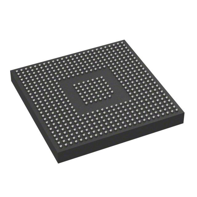
User's Manual
RZ/G2E
Overview for User’s Manual: Hardware
LSI for Rich Graphics Applications
— Preliminary —
Specifications of RZ/G2E
All information contained in these materials, including products and product specifications,
represents information on the product at the time of publication and is subject to change by
Renesas Electronics Corp. without notice. Please review the latest information published by
Renesas Electronics Corp. through various means, including the Renesas Electronics Corp.
website (http://www.renesas.com).
www.renesas.com
Rev.0.80 Feb. 2019
�Notice
1. Descriptions of circuits, software and other related information in this document are provided only to illustrate the operation of
semiconductor products and application examples. You are fully responsible for the incorporation or any other use of the circuits,
software, and information in the design of your product or system. Renesas Electronics disclaims any and all liability for any losses and
damages incurred by you or third parties arising from the use of these circuits, software, or information.
2. Renesas Electronics hereby expressly disclaims any warranties against and liability for infringement or any other claims involving patents,
copyrights, or other intellectual property rights of third parties, by or arising from the use of Renesas Electronics products or technical
information described in this document, including but not limited to, the product data, drawings, charts, programs, algorithms, and
application examples.
3. No license, express, implied or otherwise, is granted hereby under any patents, copyrights or other intellectual property rights of Renesas
Electronics or others.
4. You shall not alter, modify, copy, or reverse engineer any Renesas Electronics product, whether in whole or in part. Renesas Electronics
disclaims any and all liability for any losses or damages incurred by you or third parties arising from such alteration, modification,
copying or reverse engineering.
5. Renesas Electronics products are classified according to the following two quality grades: “Standard” and “High Quality”. The intended
applications for each Renesas Electronics product depends on the product’s quality grade, as indicated below.
“Standard”:
Computers; office equipment; communications equipment; test and measurement equipment; audio and visual equipment;
home electronic appliances; machine tools; personal electronic equipment; industrial robots; etc.
“High Quality”: Transportation equipment (automobiles, trains, ships, etc.); traffic control (traffic lights); large-scale communication
equipment; key financial terminal systems; safety control equipment; etc.
Unless expressly designated as a high reliability product or a product for harsh environments in a Renesas Electronics data sheet or other
Renesas Electronics document, Renesas Electronics products are not intended or authorized for use in products or systems that may pose a
direct threat to human life or bodily injury (artificial life support devices or systems; surgical implantations; etc.), or may cause serious
property damage (space system; undersea repeaters; nuclear power control systems; aircraft control systems; key plant systems; military
equipment; etc.). Renesas Electronics disclaims any and all liability for any damages or losses incurred by you or any third parties arising
from the use of any Renesas Electronics product that is inconsistent with any Renesas Electronics data sheet, user’s manual or other
Renesas Electronics document.
6. When using Renesas Electronics products, refer to the latest product information (data sheets, user’s manuals, application notes, “General
Notes for Handling and Using Semiconductor Devices” in the reliability handbook, etc.), and ensure that usage conditions are within the
ranges specified by Renesas Electronics with respect to maximum ratings, operating power supply voltage range, heat dissipation
characteristics, installation, etc. Renesas Electronics disclaims any and all liability for any malfunctions, failure or accident arising out of
the use of Renesas Electronics products outside of such specified ranges.
7. Although Renesas Electronics endeavors to improve the quality and reliability of Renesas Electronics products, semiconductor products
have specific characteristics, such as the occurrence of failure at a certain rate and malfunctions under certain use conditions. Unless
designated as a high reliability product or a product for harsh environments in a Renesas Electronics data sheet or other Renesas
Electronics document, Renesas Electronics products are not subject to radiation resistance design. You are responsible for implementing
safety measures to guard against the possibility of bodily injury, injury or damage caused by fire, and/or danger to the public in the event
of a failure or malfunction of Renesas Electronics products, such as safety design for hardware and software, including but not limited to
redundancy, fire control and malfunction prevention, appropriate treatment for aging degradation or any other appropriate measures.
Because the evaluation of microcomputer software alone is very difficult and impractical, you are responsible for evaluating the safety of
the final products or systems manufactured by you.
8. Please contact a Renesas Electronics sales office for details as to environmental matters such as the environmental compatibility of each
Renesas Electronics product. You are responsible for carefully and sufficiently investigating applicable laws and regulations that regulate
the inclusion or use of controlled substances, including without limitation, the EU RoHS Directive, and using Renesas Electronics
products in compliance with all these applicable laws and regulations. Renesas Electronics disclaims any and all liability for damages or
losses occurring as a result of your noncompliance with applicable laws and regulations.
9. Renesas Electronics products and technologies shall not be used for or incorporated into any products or systems whose manufacture, use,
or sale is prohibited under any applicable domestic or foreign laws or regulations. You shall comply with any applicable export control
laws and regulations promulgated and administered by the governments of any countries asserting jurisdiction over the parties or
transactions.
10. It is the responsibility of the buyer or distributor of Renesas Electronics products, or any other party who distributes, disposes of, or
otherwise sells or transfers the product to a third party, to notify such third party in advance of the contents and conditions set forth in this
document.
11. This document shall not be reprinted, reproduced or duplicated in any form, in whole or in part, without prior written consent of Renesas
Electronics.
12. Please contact a Renesas Electronics sales office if you have any questions regarding the information contained in this document or
Renesas Electronics products.
(Note 1) “Renesas Electronics” as used in this document means Renesas Electronics Corporation and also includes its directly or indirectly
controlled subsidiaries.
(Note 2) “Renesas Electronics product(s)” means any product developed or manufactured by or for Renesas Electronics.
(Rev.4.0-1
November 2017)
�General Precautions in the Handling of Microprocessing Unit and Microcontroller Unit Products
The following usage notes are applicable to all Microprocessing unit and Microcontroller unit products from Renesas.
For detailed usage notes on the products covered by this document, refer to the relevant sections of the document as well
as any technical updates that have been issued for the products.
1. Handling of Unused Pins
Handle unused pins in accordance with the directions given under Handling of Unused Pins in the
manual.
⎯ The input pins of CMOS products are generally in the high-impedance state. In operation with an
unused pin in the open-circuit state, extra electromagnetic noise is induced in the vicinity of LSI, an
associated shoot-through current flows internally, and malfunctions occur due to the false
recognition of the pin state as an input signal become possible. Unused pins should be handled as
described under Handling of Unused Pins in the manual.
2. Processing at Power-on
The state of the product is undefined at the moment when power is supplied.
⎯ The states of internal circuits in the LSI are indeterminate and the states of register settings and
pins are undefined at the moment when power is supplied.
In a finished product where the reset signal is applied to the external reset pin, the states of pins
are not guaranteed from the moment when power is supplied until the reset process is completed.
In a similar way, the states of pins in a product that is reset by an on-chip power-on reset function
are not guaranteed from the moment when power is supplied until the power reaches the level at
which resetting has been specified.
3. Prohibition of Access to Reserved Addresses
Access to reserved addresses is prohibited.
⎯ The reserved addresses are provided for the possible future expansion of functions. Do not access
these addresses; the correct operation of LSI is not guaranteed if they are accessed.
4. Clock Signals
After applying a reset, only release the reset line after the operating clock signal has become stable.
When switching the clock signal during program execution, wait until the target clock signal has
stabilized.
⎯ When the clock signal is generated with an external resonator (or from an external oscillator)
during a reset, ensure that the reset line is only released after full stabilization of the clock signal.
Moreover, when switching to a clock signal produced with an external resonator (or by an external
oscillator) while program execution is in progress, wait until the target clock signal is stable.
5. Differences between Products
Before changing from one product to another, i.e. to a product with a different part number, confirm
that the change will not lead to problems.
⎯ The characteristics of Microprocessing unit or Microcontroller unit products in the same group but
having a different part number may differ in terms of the internal memory capacity, layout pattern,
and other factors, which can affect the ranges of electrical characteristics, such as characteristic
values, operating margins, immunity to noise, and amount of radiated noise. When changing to a
product with a different part number, implement a system-evaluation test for the given product.
�Under Development
Preliminary
Specifications in this document are tentative and subject to change.
RZ/G2E
RZ/G Series, 2nd Generation
R01UH0848EJ0080
Rev.0.80
Feb. 21, 2019
1. Overview
1.1
Introduction
The RZ/G2E includes:
•
Two 1.2-GHz Arm® Cortex®-A53 MPCore™ cores,
•
Memory controller for DDR3L-1856 * with 32 bits × 1 channel,
•
1 channel for RGB888 output and 2 channels for LVDS,
•
1 channel MIPI-CSI2 Video Input, 2channels digital Video Input,
•
USB3.0 × 1ch and USB2.0 × 1ch interfaces,
•
800-MHz Arm® Cortex®-R7 core (option),
•
Three-dimensional graphics engines,
•
Sound processing units,
•
SD card host interface,
•
PCI Express interface,
•
Video processing units,
•
CAN interface, and
•
EthernetAVB interface.
* : The “DDR3L-1856” indicates the DDR3L-SDRAM bus interface which operates at a frequency of 928 MHz in this
manual.
Note: Arm and Cortex are registered trademark of Arm Limited. All other brands or product names are the property of
their respective holders.
Remarks: For items noted as "option", please contact a Renesas Electronics sales representative.
1.2
1.2.1
List of Specifications
Arm Core
Item
Description
System CPU Cortex-A53
• Arm Cortex-A53 Dual MPCore 1.2GHz
• L1 I/D cache 32/32 KBytes (Parity/ECC), L2 cache 256 Kbytes (ECC)
• NEON™/VFPv4 supported
• Security extension supported
• Virtualization supported
• Armv8 architecture
Debug and Trace
• JTAG/SWD I/F supported
• ETM-A53 supported
• ETF 16 KBytes for program flow trace (each cluster)
R01UH0848EJ0080 Rev.0.80
Feb. 21, 2019
1-1
�Under Development
RZ/G Series, 2nd Generation
RZ/G2E
1.2.2
1. Overview
CPU Core Peripherals
Item
Clock Pulse Generator (CPG)
Description
• Generates the clocks from external clock (EXTAL).
Maximum Cortex-A53 clock: 1.2 GHz
Maximum 3DGE clock: 600 MHz
Maximum AXI-bus clock: 266 MHz
Maximum SDRAM bus clock: 928 MHz (DDR3L-1856)
Maximum media clock: 266 MHz
System Controller (SYSC)
•
System-CPU shut down mode control supported
•
Module-standby mode supported
•
Includes module reset registers to control reset operation of individual on-chip
peripheral modules
• Shuts down and restores power to target modules.
Target modules:
— Cortex-A53 (with independent shutting down of CPUs 0, 1 and SCU+L2 cache) *
* : SCU and L2 cache are treated as one power-domain. When CPU is working,
SCU+L2 cache can't be powered off.
• Low leakage standby mode supported.
RESET
• Includes one reset-signal external output port for external modules
• Includes Boot Address Register etc.
Pin function controller (PFC)
• Setting multiplexed pin functions for LSI pins
Function of the LSI pin selectable by setting the registers in the PFC module
• Module selection
Enable and disable the functions of LSI pins to which pin functions from multiple pin
groups are assigned by setting the registers in the PFC module.
• Pull-up/down control for each LSI pin
On/off and up/down of the pull register on each LSI pin can be controlled by setting
the registers in the PFC module.
•
General-purpose I/O (GPIO)
Control of SDIO functions
SDIO functions, including the driving ability of pins for the SDIF, can be controlled
by setting registers of the PFC.
• General-purpose I/O ports
• Supports GPIO interrupts
Thermal sensor (THS)
•
1 channel of thermal sensor
• Programmable 3 temperature level for the sensor, to indicate the temperature level
• Interrupt when the temperature reaches programmed
R01UH0848EJ0080 Rev.0.80
Feb. 21, 2019
1-2
�Under Development
RZ/G Series, 2nd Generation
RZ/G2E
1.2.3
1. Overview
External Bus Module
Item
Description
External Bus
Controller for EXBus (LBSC)
• EX-BUS interface: max. 16-bit bus
• Frequency: 66 MHz
• External area divided into several areas and managed
— Allocation to space of area 0, area 1.
— Area 0 supports 1-MByte memory space (startup mode).
— I/F settings, bus width settings, and wait state insertion are possible for each area
• SRAM interface
— Wait states can be inserted through register settings
Period of waiting is set in cycle unit, and the maximum value is 15.
— EX_WAIT pin can be used for wait state insertion
— Connectable bus widths: 16 bits or 8 bits
• Supports external buffer enable/direction control
• Supports Burst ROM interface
• Supports Byte-control SRAM interface
External Flash
Controller
• Supports RPC-IF (Reduced Pin Count interface) flash memory or QSPI flash memory
Maximum Frequency 150 MHz (300MB/s) for RPC-IF, 80 MHz (80MB/s) for QSPI (QSPI0)
Dual QSPI operation for two 4-bit serial flash memories is also available; 80 MHz (160MB/s) for
Dual QSPI (QSPI0+QSPI1).
External Bus
Controller for
DDR3L SDRAM
(DBSC4)
• DDR3L-1856 can be connected directly.
• 1 channel (32-bit bus mode)
• Memory Size: Up to 2GB
• Auto Refresh/Self Refresh/Partial Array Self Refresh supported
• Auto Pre-charge Mode
• DDR Back Up supported
• Cache memory for DDR-Memory access efficiency
• Memory access protection for secure/safety regions
• Decompression of visual near lossless compressed image
• ECC supported
R01UH0848EJ0080 Rev.0.80
Feb. 21, 2019
1-3
�Under Development
RZ/G Series, 2nd Generation
RZ/G2E
1.2.4
1. Overview
Internal Bus Module
Item
Description
AXI-bus
• On-chip main bus
— Bus protocol: AXI3 with QoS control
— Frequency: 266 MHz
— Bus width: 256 bits/128 bits/64 bits
• On-chip CPU bus
— Bus protocol: AXI3
— Frequency: 533 MHz
— Bus width: 128 bits
Direct Memory Access
Controller for System
(SYS-DMAC)
• 16 channels for PERW domain (SYDM0)
• 32 channels for PERE domain (SYDM1, 2)
• Address space: 4 GBytes on architecture
• Data transfer length: Byte, word (2 Bytes), longword (4 Bytes), 8 Bytes, 16 Bytes, 32 Bytes
and 64 Bytes
• Maximum number of transfer times: 16,777,215 times
• Transfer request:
Selectable from on-chip peripheral module request and auto request
• Bus mode:
Selectable from normal mode and slow mode
• Priority: Selectable from fixed channel priority mode and round-robin mode
• Interrupt request: Supports interrupt request to CPU at the end of data transfer
• Repeat function: Automatically resets the transfer source, destination, and count at the
end of DMA transfer (by descriptor function)
• Descriptor function (each channel) supported
• MMU (each channel) supported
• Channel bandwidth arbiter (each channel)
Boot
• System startup with selectable boot mode at power-on reset
• Either external ROM boot (area 0) or on-chip ROM boot can be selected through MD pin
on development chip.
• In on-chip ROM boot, RPC-IF or QSPI serial ROM boot is supported.
• Program downloaded to internal memory (System RAM)
• Autorun function for the downloaded program
• About detail information of BOOT, refer to Section 19 (Boot) and Appendix B (Active
sequence).
R01UH0848EJ0080 Rev.0.80
Feb. 21, 2019
1-4
�Under Development
RZ/G Series, 2nd Generation
RZ/G2E
1. Overview
Item
Description
Direct Memory Access
Controller for Audio
(Audio-DMAC)
• 16 channels
• asdm0: 16 channels
• Address space: 4 GBytes on architecture
• Data transfer length: Byte, word (2 Bytes), longword (4 Bytes), 8 Bytes, 16 Bytes, 32 Bytes
and 64 Bytes
• Maximum number of transfer times: 16,777,215 times
• Transfer request:
Selectable from on-chip peripheral module request and auto request
• Bus mode:
Selectable from normal mode and slow mode
• Priority: Selectable from fixed channel priority mode and round-robin mode
• Interrupt request: Supports interrupt request to CPU at the end of data transfer
• Repeat function: Automatically resets the transfer source, destination, and count at the
end of DMA transfer (by descriptor function)
• Descriptor function (each channel) supported
• MMU (each channel) supported
• Channel bandwidth arbiter (each channel)
Audio-DMACPeripheral-Peripheral
• Audio-DMAC (for transfer from Peripheral to Peripheral)
• 29 (extended) channels for audio domain
• Data transfer length: longword (4 Bytes)
• Transfer count: Transfer count is not specified (DMA transfer is made from the transferstart to transfer-stop settings.)
• Transfer request:
Selectable from on-chip audio peripheral module request
• Priority: round-robin mode
• Interrupt request: not supports interrupt request to CPU at the end of data transfer
IPMMU
• An IPMMU is a memory management unit (MMU) which provides address translation and
access protection functionalities to processing units and interconnect networks.
Interrupt Controller
(INTC)
INTC-AP
(For AP-System core
Cortex-A53)
— 7 interrupt pins which can detect external interrupts
— Max. 480 shared peripheral interrupts supported
— Fall/rise/high level/low level detection is selectable
— On-chip peripheral interrupts: Priority can be specified for
each module
— 16 software interrupts that have been generated and 6
private peripheral interrupts supported
— 32-level priority selectable
— Trust Zone supported
1.2.5
Internal Memory
Item
Description
System RAM
R01UH0848EJ0080 Rev.0.80
Feb. 21, 2019
RAM of 128 KBytes
1-5
�Under Development
RZ/G Series, 2nd Generation
RZ/G2E
1.2.6
1. Overview
Graphics Units
Item
Description
3D Graphics Engine
(3DGE)
• Imagination Technologies PowerVR Series 8XE GE8300
• Max. Freq. 600 MHz
• Drastically performance improvements for sophisticated graphics and GPU computer
• Reducing power consumption even further through advanced power saving
mechanisms
• Lowest memory bandwidth in the industry with compression technologies
• Ultra HD deep color GPU Support APIs: OpenGL ES 3.1, (OpenCL 1.2 EP)
• 2.4Gpix/s 200Mpoly/s 19.2GFLOPS
R01UH0848EJ0080 Rev.0.80
Feb. 21, 2019
1-6
�Under Development
RZ/G Series, 2nd Generation
RZ/G2E
1. Overview
Item
Description
Display Unit (DU)
Display channel
2 independently controllable channels
Interface
• LVDS 2 channels
• Digital RGB 1channel
(8-bit precision for each RGB color)
LVDS interface (per channel)
• Output: compliant with TIA/EIA-644; five pairs of
differential output (four pairs of data and one pair
of clock)
• Operating frequency: Dotclk 148.5 MHz
Screen size and number of
composite planes per channel
• Maximum screen size: 1920 × 1080 (also depends
on frame rate)
• Number of planes specifiable: 5 (VSP2
processing)
• Number of planes specifiable: 1 (DU)
CRT scanning method
Non-interlaced
Synchronization method
Master
Internal color palette (VSP2)
• Includes four color palette planes which can
display 256 of 260 thousands colors at the same
time.
Output display numbers
• Two output channels
• 8-bit precision for each RGB color
Video Input Module (VIN)
Blending ratio settings (VSP2)
Number of color palette planes with blending ratio: 4
Dot clock
Switchable between external input and internal clock
MIPI-CSI2 interface
•
1 channel (2lane × 1 channel)
• Interleaving by 2 VC (virtual channel) supported
• Filtering by DT (data type) supported
• YUV422 8/10bit, RGB888, Embedded 8bit, User Defined 8bit
are supported
• 1.1Gbps/Lane
digital interface
• 2 channels (RGB/YCbCr)
• Dotclk 100 MHz
• ITU-R BT.601 interface: 8-, 10- (same size only (not scaling)),
or 12-bit (same size only (not scaling)) YCbCr422, RGB666,
RGB888
• ITU-R BT.656 interface: 8-, 10- (same size only (not scaling)),
or 12-bit (same size only (not scaling)) YCbCr422
• ITU-R BT.1358 interface: 16-, 20- (same size only (not
scaling)), or 24-bit (same size only (not scaling)) YCbCr422
• ITU-R BT.709 interface: 8-, 10- (same size only (not scaling)),
or 12-bit (same size only (not scaling)) YCbCr422, RGB666,
RGB888
Capturing function
Up to 2 input images can be captured (using VC, DT filtering)
Clipping function
Up to 4096 × 4096
Horizontal scaling
Up to two times, but only scaling down is possible for HD1080i or
HD1080p data. (one input only)
Vertical scaling
R01UH0848EJ0080 Rev.0.80
Feb. 21, 2019
Up to three times, but only scaling down is possible for HD1080i
or HD1080p data. (one input only)
1-7
�Under Development
RZ/G Series, 2nd Generation
RZ/G2E
1. Overview
Item
Description
Video Input Module (VIN)
1.2.7
Output format
RGB-565, ARGB-1555, ARGB8888, YCbCr422, RGB888,
YCbCr420 YC separation, and extraction of the Y component
Video Processing
Item
Description
Video Signal Processor
(VSPI)
VSPI has the following features. 1 set of VSPI is integrated.
125 Mpix/s process rate per 1 VSPI
Supports Full HD (1920 pixels × 1080 lines) processing
(1) Supports Various Data Formats and Conversion
— Supports YCbCr444/422/420, RGB, αRGB, αplane
— Color space conversion and changes to the number of colors by dithering
— Color keying
— Supports combination between pixel alpha and global alpha
— Supports generating pre multiplied alpha
(2) Video Processing
— Up and down scaling with arbitrary scaling ratio
— Super resolution processing
— Image rotation/reversal function: Reverses an image vertically/horizontally or
rotates it by 90°/270°
(3) Picture Quality/Color Correction with 1D/3D Look Up Table (LUT)
— Hue, brightness, and saturation adjustment
— 1D and 2D histogram
Following functions will be supported by Renesas software portfolio.
— Dynamic γ correction and gain correction
— Correction of color (to adjust skin tones or colors in memory)
(4) Visual near lossless image compression supported
— 50% of bandwidth is diminished
R01UH0848EJ0080 Rev.0.80
Feb. 21, 2019
1-8
�Under Development
RZ/G Series, 2nd Generation
RZ/G2E
1. Overview
Item
Description
Video Signal Processor
(VSPB)
VSPB has the following features. 1 set of VSPB is integrated.
125 Mpix/s process rate (output rate) per 1 VSPB.
Supports Full HD (1920 pixels × 1080 lines) processing
(1) Supports Various Data Formats and Conversion
— Supports YCbCr444/422/420, RGB, αRGB, αplane
— Color space conversion and changes to the number of colors by dithering
— Color keying
— Supports combination between pixel alpha and global alpha
— Supports generating pre multiplied alpha
(2) Video Processing
— Blending of 5 picture layers and raster operations (ROPs)
— Vertical flipping
(3) Picture Quality/Color Correction with 1D/3D Look Up Table (LUT)
— 1D and 2D histogram
Following functions will be supported by Renesas software portfolio.
— Dynamic γ correction and gain correction
— Correction of color (to adjust skin tones or colors in memory)
(4) Visual near lossless image compression supported
— 50% of bandwidth is diminished
Video Signal Processor
(VSPD)
VSPD has the following features. 2 sets of VSPD are integrated.
Supports Full HD (1920 pixels × 1080 lines) resolution.
(1) Supports Various Data Formats and Conversion
— Supports YCbCr444/422/420, RGB, αRGB, αplane
— Color space conversion and changes to the number of colors by dithering
— Color keying
— Supports combination between pixel alpha and global alpha
— Supports generating pre multiplied alpha
(2) Video processing
— Blending of 5 picture layers and raster operations (ROPs)
— Vertical flipping in case of output to memory
(3) Direct connection to display module
— Supports 2048 pixels in horizontal direction
— Writing back image data which is transferred to Display Unit (DU) to memory
R01UH0848EJ0080 Rev.0.80
Feb. 21, 2019
1-9
�Under Development
RZ/G Series, 2nd Generation
RZ/G2E
1. Overview
Item
Description
Video Codec Processor
(VCP4)
The VCP4 is a multi-codec module which provides encoding and decoding capabilities
on the basis of multiple video coding schemes, e.g., H.265/HEVC, H.264/AVC.
This IP (Intellectual Property) is a multi codec that processes the frame or each field by
controlling software for VCP4 executed on host CPU.
• The VCP4 has the following features: Support for multiple codecs
H.265/HEVC MP (Main Profile) decoding
H.264/MPEG-4 AVC HP (High Profile) and MVC SHP (Stereo High Profile) encoding
and decoding
• Support for up to 4K resolutions (H.265 and H.264)
Multiple channel processing:
When iVDP1C is not used:
(H.264/H.265 1920 × 1080p × 60 fps)
When iVDP1C is used:
(H.264/H.265 1920 × 1080p × 30 fps)
Note:
“1920 × 1080p × 120 fps” can be replaced as “3840 × 2160p × 30 fps”.
“1920 × 1080p × 60 fps” can be replaced as “1280 × 720p × 120 fps”.
“1920 × 1080p × 30 fps” can be replaced as “1280 × 720p × 60 fps”.
Maximum performance will change with securable bus bandwidth.
•
Data handling on a picture-by-picture basis
Encodes/decodes data one picture (frame or field) at a time.
• High picture quality
Supports the H.264 high-efficiency coding tools (CABAC, 8 × 8 frequency
conversion, and quantization matrix).
High-efficiency motion vector detection by a combination of discrete search and
trace search
Optimal-mode selection by Rate-Distortion (RD) cost evaluation
Picture quality control based on activity analysis results which match visual models
• Low power dissipation
Dynamically disables the clocks for the entire VCP4.
Dynamically disables the clocks for individual submodules.
• Includes its own reference data cache
• Lossless image compression for reference picture is supported
Use the software from Renesas to handle VCP4 functions.
Video Decoding Processor
for inter-device video transfer
• Low-latency decoder H.264/AVC, JPEG
(iVDP1C)
• Bit depth 8/10/12bits
• Color format 4:2:0/4:2:2
• Performance:
1280 pixels × 960 lines × 30 frames/second × 2 channels
(when VCP4 is not used)
1280 pixels × 960 lines × 30 frames/second × 1 channel
(when VCP4 is used)
• Max resolution:
1920 pixels × 1088 lines
• Includes its own reference data cache
• Lossless image compression for reference picture is supported if bit depth is 8 bits
Use the software from Renesas to handle iVDP1C functions.
R01UH0848EJ0080 Rev.0.80
Feb. 21, 2019
1-10
�Under Development
RZ/G Series, 2nd Generation
RZ/G2E
1. Overview
Item
Description
Fine Display Processor
(FDP1)
The FDP1 is the de-interlacing module which converts the interlaced video to
progressive video, and has the following features.
(1) Supports 1 channel
125 Mpix/s for output performance per 1 FDP1
(2) Supports various data formats
— Input: YCbCr444/422/420
— Output: YCbCr444/422/420 and RGB/αRGB
(3) 8190 pixels x 8190 lines video processing performance
(4) High image quality de-interlacing algorithm
— Motion adaptive de-interlacing
— Accurate still detection
— Diagonal line interpolation (DLI)
(5) Visual near lossless image compression supported
50% of bandwidth is diminished
R01UH0848EJ0080 Rev.0.80
Feb. 21, 2019
1-11
�Under Development
RZ/G Series, 2nd Generation
RZ/G2E
1.2.8
1. Overview
Sound Interface
Item
Description
Sampling Rate Converter
Unit (SCU)
Overall
specification
• Includes ten SRC modules
— Supports the quality suitable for audio sound (High-soundquality type) (THD+N -132dB): six modules
— Supports the quality suitable for voice sound (general-soundquality type) (THD+N -96dB): four modules
• The SRC module is capable of correcting phase change and delay
(timing jitter) generated during data transfer over external
memories or external devices.
• The channel count conversion unit (CTU), mixer (MIX), and digital
mute and volume function (DVC) can be used on two fixed output
channels.
Sampling rate
conversion
(SRC)
• Capable of asynchronous sampling rate conversion
• Supports resolutions up to 24 bits
• Two kinds of filter type for SRC.
— Supports the quality suitable for audio sound (High-soundquality type) (THD+N -132dB): Realized the filter by passband
-1dB@0.4575FS, cutoff -18dB@0.5FS.
— Supports the quality suitable for voice sound (general-soundquality type) (THD+N -96dB): Realized the filter by passband 1dB@0.4561FS, cutoff -72dB@0.5FS. (Characteristics of each
filter is written in the equivalent/up-sampling cases.)
• Automatically generates antialiasing filter coefficients
• For monaural to eight-channel sound sources
Channel count
conversion
unit (CTU)
• Downmixing and splitter functions
— Conversion of eight input channels into four output channels
— Conversion of six input channels into two output channels
— Conversion of two input channels into four sets of two output
channels
— Conversion of one input channel into eight sets of one output
channel
— No conversion
Mixer (MIX)
• Mixing (adds) two to four sources into one
• Ratio for adding sources is selectable
• Ratio is dynamically changeable
• Mixing with volume ramp is available (ramp period is selectable)
Digital volume
and mute
• Volume control function including digital volume, volume ramp,
and zero-crossing mute
function (DVC)
• The digital volume function is specified by a 24-bit fixed-point
value within the range from 0 to 8 times (mute, or -120 to 18 dB)
• The volume ramp function can be used for soft mute, fade-in,
fade-out, or desired volume adjustment
• The volume ramp period can be changed within the sampling
range from the 0th to 23rd power of 2
• The zero-crossing mute function silences the sound at the zerocrossing point of the audio data
R01UH0848EJ0080 Rev.0.80
Feb. 21, 2019
1-12
�Under Development
RZ/G Series, 2nd Generation
RZ/G2E
1. Overview
Item
Description
Serial Sound Interface Unit
(SSIU)
Overall
specification
• Includes ten SSI modules functioning as interfaces with external
devices.
— Supports short and long formats for monaural
— Supports TDM format (six modules of ten modules can be
used for this function)
• Max. 8 independent monaural sound sources in a TDM format can
be in TDM format.
Serial sound
interface (SSI)
• 10 channels
• Max SCK frequency 15.1 MHz (for slave input) or 12.5 MHz (for
master output)
• Operating mode: non-compressed mode (Not support compressed
mode)
• Supports versatile serial audio formats (I2S/left justified/right
justified)
• Supports master/slave functions
• Programmable word clock, bit clock generation functions
• Multichannel format functions (up to four channels)
• Supports 8-/16-/18-/20-/22-/24-bit data formats
• Supports TDM mode
• Supports WS continue mode
• The DMA controller or interrupts control the transfer of data to and
from the SSI module.
• Supports short and long frames for monaural data (valid data
lengths are 8 and 16 bits)
• Up to nine independent clock signals can be input.
Audio Clock Generator
(ADG)
R01UH0848EJ0080 Rev.0.80
Feb. 21, 2019
Selection or division of audio clock signals
1-13
�Under Development
RZ/G Series, 2nd Generation
RZ/G2E
1.2.9
1. Overview
Storage
Item
Description
USB2.0 Host
(EHCI/OHCI)
• 1 channel (Host-Function 1channel)
• USB Host (EHCI/OHCI) 1LINK
• Compliance with USB2.0 (High-Speed)
• Interrupt request
• Internal dedicated DMA
• Compliance with Battery Charging function Rev1.2:
+ Charging Port (Host): CDP, SDP are supported (Not support DCP).
+ Portable Device (Function) is supported.
USB3.0 Host
Controller
• USB 3.0 DRD 1 channel
• This module can be use as USB2.0 as follows
Core
Super Speed
High Speed
Full Speed
Low Speed
Host
√
√
√
√
Peripheral
√
√
√
—
• Supports SS/HS/FS/LS. xHCI
SD Card Host Interface
(SDHI)
•
3 channels
• Supports SDR104 class transfer rate Does not support CPRM
• Supports SD memory/SDIO interface
• Error check function: CRC7 (command/response), CRC16 (data)
• Max Frequency 200 MHz
• Card detection function
• Supports write protection
• SD-binding function
— Compliant with Content Protection for Recordable Media Specification in revision 0.92
of the SD-Binding Part of the SD Memory Card Book
• SD-SD content protection
— Compliant with Content Protection for Recordable Media Specification in revision 0.92
of the SD-SD part of the SD Memory Card Book
Multimedia Card
Interface (MMC)
• 1 channel
• eMMC 5.0 base, Support HS400 class transfer rate
• eMMC controllable
• Data bus: 1/4/8-bit MMC mode (not support SPI mode)
• Support block transfer (not support stream transfer)
• Block size in multiple block transfer: 512 Bytes
rawNAND Controller
•
R01UH0848EJ0080 Rev.0.80
Feb. 21, 2019
The NAND Flash Memory Interface controller implements the function of a high level
interface to one NAND flash device. It supports the functionality of the high speed NAND
Flash devices described in the ONFI 1.x specifications.
1-14
�Under Development
RZ/G Series, 2nd Generation
RZ/G2E
1.2.10
1. Overview
Network
Item
Description
Controller Area
Network Interface
(CAN interface)
• 2 interfaces
• Supports CAN specification 2.0B
• Maximum bit rate: 1 Mbps
• Message box
— Normal mode: 32 receive-only mailboxes and 32 mailboxes for transmission/reception
— FIFO mode:
32 receive-only mailboxes and 24 mailboxes for transmission/reception, 4-stage FIFO
for transmission, and 4-stage FIFO for reception
• Reception
— Data frame and remote frame can be received.
— Selectable receiving ID format
— Selectable overwrite mode (message overwritten) or overrun mode (message
discarded)
• Acceptance filter
Mask can be enabled or disabled for each mailbox.
•
Transmission
— Data frame and remote frame can be transmitted.
— Selectable transmitting ID format (only standard ID, only extended ID, or both IDs)
— Selectable ID priority mode or mailbox number priority mode
• Sleep mode for reducing power consumption
• 2 interfaces
CAN-FD
• 8 Mbps (CAN clock 40 MHz)
PCIE Controller
• PCI Express Base Specification Revision 2.0
• PHY integrated
• 1 Lanes × 1 channel
EthernetAVB-IF
• Supports IEEE802.1BA, IEEE802.1AS, IEEE802.1Qav and IEEE1722 functions
• Supports transfer at 1000 Mbps and 100 Mbps
• Magic packet detection
• Supports Reception Filtering to separate streaming frames from different sources
• Supports interface conforming to IEEE802.3 PHY RGMII (Reduced Gigabit Media
Independent Interface)
• RGMII v1.3
1.2.11
Timer
Item
Description
RCLK Watchdog
Timer
• 1 channel
• Internal 16-bit watchdog timer operated by RCLK
• Programmable overflow time period: more than 1 hour count capable
16-Bit Timer Pulse
Unit (TPU)
• 4-channel 16-bit timers
• Each channel outputs PWM
R01UH0848EJ0080 Rev.0.80
Feb. 21, 2019
1-15
�Under Development
RZ/G Series, 2nd Generation
RZ/G2E
1. Overview
Item
Description
System Watchdog
Timer
• 1 channel
• Internal 16-bit watchdog timer
• Programmable overflow time period: more than 1 hour count capable
initial counter value 171[s]
Compare Match
Timer Type0 (CMT0)
• 2 channels
• 32-bit timer (16 bits/32 bits can be selected)
• Source clock: RCLK clock
• Compare match function provided
• Interrupt requests
Compare Match
Timer Type1 (CMT1)
• 8 channels
• 48-bit timer (16 bits/32 bits/48 bits can be selected)
• Source clock: RCLK/system clock
• Compare match function provided
• Interrupt requests
Compare match timer
2 (CMT2)
(same as CMT1)
Compare match timer
3 (CMT3)
(same as CMT1)
System Timer
• 32-bit timer, 1channel (16 bits/32 bits can be selected)
• Compare match function provided
• Interrupt requests
System up-time clock
• 1 channel
• Internal 32-bit timer
• Programmable overflow time period: maximum 24 hours
Timer Unit (TMU)
• 15 channels
• 32-bit timer
• Auto-reload type 32-bit down counter
• Internal prescaler
• Interrupt request
•
2 channels for input capture
R01UH0848EJ0080 Rev.0.80
Feb. 21, 2019
1-16
�Under Development
RZ/G Series, 2nd Generation
RZ/G2E
1.2.12
1. Overview
Peripheral Module
Item
Description
Trusted Secure IP
(TSIP)
• Access management unit
• Crypto engines
• Random number generator
• AES, RSA, SHA
IIC Bus Interface for
PMIC (IIC for PMIC)
• 1 PMIC channel for dedicated buffer
• Supports single master transmission/reception
• Interrupt request
• Automatic transfer by wakeup control
I2C Bus Interface
(I2C)
• 8 channels
• 2 channels for buffers with a slew rate (channel 0, 3 for dedicated buffers)
• 6 channels for LVTTL buffers (channels 1, 2, 4, 5, 6, 7 for ordinary buffers)
• NXP I2C bus interface method supported
• Master/slave functions
• Multi-master functions
• Transfer rate up to 400 kbps supported
• Programmable clock generation from the system clock
• Master and Slave function DMA supported
R01UH0848EJ0080 Rev.0.80
Feb. 21, 2019
1-17
�Under Development
RZ/G Series, 2nd Generation
RZ/G2E
Item
Description
Serial communication
interface with FIFO
(SCIF)
Overall
specification
1. Overview
• 6 channels
• Asynchronous, clock-synchronized modes
• Asynchronous serial communication mode
The SCIF performs serial data communication based on a characterby-character asynchronous system. This feature enables serial data
communication with standard asynchronous communication chips
that support Universal Asynchronous Receiver/Transmitter (UART)
or Asynchronous Communication Interface Adapter (ACIA). There is
a choice of eight serial data transfer formats.
— Data length: 7 bits or 8 bits
— Stop bits: 1 bit or 2 bits
— Parity: Even/odd/none
— Receive error detection: Parity, framing, and overrun errors
— Break detection:
A break is detected when a framing error lasts for more than 1
frame length at Space 0 (low level).
When a framing error occurs, a break can also be detected by
reading the RX pin level directly from the serial port register
(SCSPTR).
• Clock synchronous serial communication mode
The SCIF performs serial data communication synchronized with a
clock. This feature enables serial data communication with other LSIs
that support synchronous communication. There is a single serial data
communication format for clock synchronous serial communication.
— Data length: 8 bits
— Receive error detection: Overrun errors
• Full-duplex communication capability
The SCIF has an independent transmitter and receiver that enable
simultaneous transmission and reception. The transmitter and
receiver both have a 16-stage FIFO buffer structure, enabling
continuous serial data transmission and reception.
• On-chip baud rate generator, enabling any bit rate to be selected
The SCIF enables choice of a clock source for transmission/reception:
a clock from the on-chip baud rate generator based on the internal
clock or an external clock.
• Eight interrupt sources
The SCIF has eight types of interrupt sources. receive-data-ready,
receive-FIFO-data-full, break, transmit-FIFO-data-empty, transmitend, receive-error, overrun-error and time-out and enables any of
them to be requested independently.
• DMA data transfer
When the transmit FIFO register is empty or the receive FIFO
register has received data, issuing a DMA transfer request activates
the DMA controller (DMAC) to execute a data transfer.
• In asynchronous mode using channels 0, 1, 3, and 4, modem control
functions (RTS and CTS) are stored.
• RTS and CTS are not implemented for SCIF2 and SCIF5.
R01UH0848EJ0080 Rev.0.80
Feb. 21, 2019
1-18
�Under Development
RZ/G Series, 2nd Generation
RZ/G2E
Item
Description
Serial communication
interface with FIFO
(SCIF)
Overall
specification
1. Overview
• The amount of data in the transmit/receive FIFO registers and the
number of receive errors in receive data in the receive FIFO register
are available.
• In asynchronous mode, a receive data ready (DR) or a timeout error
(TO) can be detected during reception.
Clock-Synchronized
Serial Interface with
FIFO (MSIOF)
• 4 channels
• Internal 32-bit × 64-stage transmit FIFOs/internal 32-bit × 256-stage receive FIFOs
• Supports master and slave modes
• Internal prescaler
• Supports serial formats: IIS, SPI (master and slave modes)
• Interrupt request, DMAC request
High Speed Serial
Communication
Interface with FIFO
(HSCIF)
• 5 channels
• Asynchronous serial communication mode
• Capable of full-duplex communication
• On-chip baud rate generator, enabling any bit rate to be selected
• Eight interrupt sources
• DMA data transfer
• Modem control functions (HRTS# and HCTS#) are stored.
• The amount of data in the transmit/receive FIFO registers and the number of receive errors
in receive data in the receive FIFO register are available.
• A receive data ready (DR) or a timeout error (TO) can be detected during reception.
• 7 channels
PWM
• High-level width (10 bits) of PWM output can be set.
• Output cycle periods (10 bits) of PWM can be set.
• Periods in the range from two to 224 × 1023 cycles of the Pϕ clock can be set.
• Continuous pulse or single pulse output selectable
1.2.13
Others
Item
Description
Boundary Scan
(option)
• Boundary scan based on IEEE 1149.1 via JTAG interface is supported.
Note that some module pins are not available on this boundary scan.
R01UH0848EJ0080 Rev.0.80
Feb. 21, 2019
1-19
�RZ/G2E
Overview for User’s Manual: Hardware
Publication Date:
Rev.0.80
Feb. 21, 2019
Published by:
Renesas Electronics Corporation
�http://www.renesas.com
SALES OFFICES
Refer to "http://www.renesas.com/" for the latest and detailed information.
Renesas Electronics Corporation
TOYOSU FORESIA, 3-2-24 Toyosu, Koto-ku, Tokyo 135-0061, Japan
Renesas Electronics America Inc.
1001 Murphy Ranch Road, Milpitas, CA 95035, U.S.A.
Tel: +1-408-432-8888, Fax: +1-408-434-5351
Renesas Electronics Canada Limited
9251 Yonge Street, Suite 8309 Richmond Hill, Ontario Canada L4C 9T3
Tel: +1-905-237-2004
Renesas Electronics Europe Limited
Dukes Meadow, Millboard Road, Bourne End, Buckinghamshire, SL8 5FH, U.K
Tel: +44-1628-651-700
Renesas Electronics Europe GmbH
Arcadiastrasse 10, 40472 Düsseldorf, Germany
Tel: +49-211-6503-0, Fax: +49-211-6503-1327
Renesas Electronics (China) Co., Ltd.
Room 1709 Quantum Plaza, No.27 ZhichunLu, Haidian District, Beijing, 100191 P. R. China
Tel: +86-10-8235-1155, Fax: +86-10-8235-7679
Renesas Electronics (Shanghai) Co., Ltd.
Unit 301, Tower A, Central Towers, 555 Langao Road, Putuo District, Shanghai, 200333 P. R. China
Tel: +86-21-2226-0888, Fax: +86-21-2226-0999
Renesas Electronics Hong Kong Limited
Unit 1601-1611, 16/F., Tower 2, Grand Century Place, 193 Prince Edward Road West, Mongkok, Kowloon, Hong Kong
Tel: +852-2265-6688, Fax: +852 2886-9022
Renesas Electronics Taiwan Co., Ltd.
13F, No. 363, Fu Shing North Road, Taipei 10543, Taiwan
Tel: +886-2-8175-9600, Fax: +886 2-8175-9670
Renesas Electronics Singapore Pte. Ltd.
80 Bendemeer Road, Unit #06-02 Hyflux Innovation Centre, Singapore 339949
Tel: +65-6213-0200, Fax: +65-6213-0300
Renesas Electronics Malaysia Sdn.Bhd.
Unit 1207, Block B, Menara Amcorp, Amcorp Trade Centre, No. 18, Jln Persiaran Barat, 46050 Petaling Jaya, Selangor Darul Ehsan, Malaysia
Tel: +60-3-7955-9390, Fax: +60-3-7955-9510
Renesas Electronics India Pvt. Ltd.
No.777C, 100 Feet Road, HAL 2nd Stage, Indiranagar, Bangalore 560 038, India
Tel: +91-80-67208700, Fax: +91-80-67208777
Renesas Electronics Korea Co., Ltd.
17F, KAMCO Yangjae Tower, 262, Gangnam-daero, Gangnam-gu, Seoul, 06265 Korea
Tel: +82-2-558-3737, Fax: +82-2-558-5338
© 2019 Renesas Electronics Corporation. All rights reserved.
Colophon 5.2
�RZ/G Series, 2nd Generation
R01UH0848EJ0080
�