Datasheet
RAA220001
Synchronous Rectified Buck MOSFET Driver
The RAA220001 is a high frequency MOSFET driver
designed to drive upper and lower power N-channel
MOSFETs in a synchronous rectified buck converter
topology.
In the RAA220001, the upper and lower gates are
both driven to an externally applied voltage that
provides the capability to optimize applications
involving trade-offs between gate charge and
conduction losses.
An advanced adaptive shoot-through protection is
integrated to prevent both the upper and lower
MOSFETs from conducting simultaneously and to
minimize dead time. The RAA220001 has a 10kΩ
integrated high-side gate-to-source resistor to prevent
self turn-on due to high input bus dV/dt.
Features
• Dual MOSFET drives for synchronous rectified
bridge
• Advanced adaptive zero shoot-through protection
○ PHASE detection
○ LGATE detection
○ Auto-zero of rDS(ON) conduction offset effect
• Low standby bias current
• 36V internal bootstrap switcher
• Bootstrap capacitor overcharging prevention
• Integrated high-side gate-to-source resistor to
prevent from self turn-on due to high input bus dV/dt
This driver also has an overvoltage protection feature
that is operational while VCC is below the POR
threshold. The PHASE node is connected to the gate
of the low-side MOSFET (LGATE) through a 30kΩ
resistor, limiting the output voltage of the converter
close to the gate threshold of the low-side MOSFET.
This design is dependent on the current being
shunted, which provides some protection to the load
should the upper MOSFET(s) become shorted.
• Pre-POR overvoltage protection for start-up and
shutdown
Applications
• Pb-free (RoHS compliant)
• High light-load efficiency voltage regulators
Related Literature
• Core regulators for advanced microprocessors
For a full list of related documents, visit our website:
• High current DC/DC converters
• RAA220001 device page
• Power rails undervoltage protection
• Expandable bottom copper pad for enhanced heat
sinking
• Dual flat no-lead (DFN) package
• Near chip-scale package footprint; improves PCB
efficiency and thinner in profile
VCC
BOOT
Pin 6
UGATE
+5V
40k
10k
POR/
Control
Logic
PHASE
ShootThrough
Protection
PWM
30k
Pin 7
22.4k
VCC
Pins 6 and 7 must be
tied together
LGATE
GND
Figure 1. Block Diagram
R16DS0005EU0100 Rev.1.00
Jul.11.19
Page 1 of 15
�RAA220001
1.
1. Overview
Overview
1.1
Typical Applications
EN0
RGND0
VSEN0
PG0
TEMP0
VCC
3.3V
1µF
3300pF
47pF
22k
PWM0
CS0
CSRTN0
VCCS
10µF
RAA220002
PWM0
PHASE0
VIN
UGATE0
BOOT0
12V
VCC12
VINSEN
12V
GND
0.1µF
12V
VCC12
NTC 10k
LGATE0
PHASE1
VCORE
COUT
VIN
UGATE1
BOOT1
PSYSIN
PWM1
PWM1
LGATE1
CS1
CSRTN1
PWM2
CS2
CSRTN2
RAA220002
PWM0
RAA229001
PHASE0
VIN
UGATE0
BOOT0
12V
VCC12
LGATE0
GND
12V
VCC12
SVCLK
GP0
BOOT1
PWM1
PWM3
LGATE1
CS3
CSRTN3
VIN
RAA220001
nVRHOT
VCC
12V
GND
CFP
VIN
UGATE1
SVDATA
nSVALERT
PHASE1
PWM4
PWM
BOOT UGATE
PHASE
LGATE
CS4
CSRTN4
PMSCL
PMSDA
nPMALERT
PWM5
CS5
CSRTN5
PWM6
CS6
CSRTN6
RAA220002
PWM0
PHASE0
VIN
UGATE0
BOOT0
12V
VCC12
LGATE0
COUT
GND
ADDR
12V
VCC12
PHASE1
UGATE1
VGT
VIN
NTC 10k
BOOT1
PWM1
PWM7
LGATE1
CS7
CSRTN7
TEMP1
47pF
22k
PG1
EN1
RGND1
VSEN1
3300pF
Figure 2. Intel 5+2 with Single-Dual Driver
R16DS0005EU0100 Rev.1.00
Jul.11.19
Page 2 of 15
�RAA220001
3.3V
1. Overview
EN0
RGND0
VSEN0
PG0
TEMP0
VCC
1µF
3300pF
47pF
22k
PWM0
CS0
CSRTN0
VCCS
10µF
RAA220002
PWM0
PHASE0
V IN
UGATE0
BOOT0
12V
12V
VCC12
VINSEN
GND
0.1µF
12V
VCC12
NTC 10k
LGATE0
PHASE1
COUT
VIN
VDD1
UGATE1
BOOT1
PWM1
PWM1
LGATE1
RAA220002
PWM0
PHASE0
CS1
CSRTN1
PWM2
CS2
CSRTN2
RAA229004
V IN
UGATE0
BOOT0
VDDIO
1.8V
12V
VCC12
12V
VCC12
0.1µF
LGATE0
GND
SVC
PWROK
BOOT1
PWM1
PWM3
LGATE1
CS3
CSRTN3
V IN
RAA220001
nVRHOT
CFP
VIN
UGATE1
SVD
SVT
PHASE1
12V
PWM4
VCC
GND
BOOT UGATE
PWM
LGATE
PHASE
CS4
CSRTN4
PMSCL
PMSDA
nPMALERT
PWM5
CS5
CSRTN5
PWM6
CS6
CSRTN6
RAA220002
PWM0
PHASE0
V IN
UGATE0
BOOT0
12V
VCC12
LGATE0
COUT
GND
ADDR
12V
VCC12
PHASE1
UGATE1
VDD2
VIN
NTC 10k
BOOT1
PWM1
PWM7
LGATE1
CS7
CSRTN7
TEMP1
47pF
22k
PG1
RGND1
VSEN1
3300pF
Figure 3. AMD 5+2 with Single-Dual Driver
R16DS0005EU0100 Rev.1.00
Jul.11.19
Page 3 of 15
�RAA220001
1.2
1. Overview
Ordering Information
Part Number
(Notes 2, 3)
Part
Marking
RAA220001GNP#HA0
001
Temp. Range
(°C)
Tape and Reel
(Units) (Note 1)
-40 to +85
6k
Package
(RoHS Compliant)
8 Ld 2x2 DFN
Pkg.
Dwg. #
L8.2x2D
Notes:
1. See TB347 for details about reel specifications.
2. These Pb-free plastic packaged products employ special Pb-free material sets, molding compounds/die attach materials, and 100% matte
tin plate plus anneal (e3 termination finish, which is RoHS compliant and compatible with both SnPb and Pb-free soldering operations).
Pb-free products are MSL classified at Pb-free peak reflow temperatures that meet or exceed the Pb-free requirements of IPC/JEDEC
J-STD-020.
3. For Moisture Sensitivity Level (MSL), see the RAA220001 device page. For more information about MSL, see TB363.
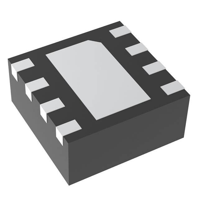
1.3
Pin Configuration
8 Ld 2x2 DFN
Top View
1.4
UGATE
1
8
PHASE
BOOT
2
7
VCC
PWM
3
6
VCC
GND
4
5 LGATE
GND
Functional Pin Descriptions
Pin
Number
Pin
Name
1
UGATE
Upper gate drive output. Connect to gate of high-side power N-channel MOSFET.
2
BOOT
Floating bootstrap supply pin for the upper gate drive. Connect the bootstrap capacitor between this pin and the
PHASE pin. The bootstrap capacitor provides the charge to turn on the upper MOSFET. See “Internal Bootstrap
Device” on page 8 for guidance in choosing the capacitor value.
3
PWM
The PWM signal is the control input for the driver. The PWM signal can enter three distinct states during operation, see
“Three-State PWM Input” on page 8 for more details. Connect this pin to the PWM output of the controller.
4
GND
Bias and reference ground. All signals are referenced to this node. It is also the power ground return of the driver.
5
LGATE
6, 7
VCC
The two VCC pins must tie to each other. Connect them to 12V bias supply. Place a high quality low ESR ceramic
capacitor from this pin to GND.
8
PHASE
Connect this pin to the SOURCE of the upper MOSFET and the DRAIN of the lower MOSFET. This pin provides a
return path for the upper gate drive.
-
PAD
Function
Lower gate drive output. Connect to gate of the low-side power N-channel MOSFET.
Connect this pad to the power ground plane (GND) using a thermally enhanced connection.
R16DS0005EU0100 Rev.1.00
Jul.11.19
Page 4 of 15
�RAA220001
2.
2. Specifications
Specifications
2.1
Absolute Maximum Ratings
Parameter
Minimum
Maximum
Unit
Supply Voltage (VCC)
15
V
BOOT Voltage (VBOOT - GND)
36
V
GND - 0.3
7
V
VPHASE - 0.3VDC
VBOOT + 0.3
V
VPHASE - 3.5
(
很抱歉,暂时无法提供与“RAA220001GNP#HA0”相匹配的价格&库存,您可以联系我们找货
免费人工找货- 国内价格 香港价格
- 6000+4.743306000+0.61450