Datasheet
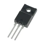
RJK6012DPP-A0
R07DS1420EJ0102
Rev.1.02
Nov.15.2019
600V - 10A - MOS FET
High Speed Power Switching
Features
Low on-resistance
RDS(on) = 0.77 typ. (at ID = 5 A, VGS = 10 V, Ta = 25 C)
Low leakage current
High speed switching
Quality grade: Standard
Outline
RENESAS Package code: PRSS0003AP-A
(Package name: TO-220FPA)
D
1. Gate
2. Drain
3. Source
G
1
2 3
S
Absolute Maximum Ratings
(Ta = 25 C)
Item
Drain to source voltage
Gate to source voltage
Drain current
Drain peak current
Body-drain diode reverse drain current
Body-drain diode reverse drain peak current
Avalanche current
Avalanche energy
Channel dissipation
Channel temperature
Storage temperature
Note:
Symbol
VDSS
VGSS
ID Note4
IDR (pulse) Note1
IAP Note3
EAR Note3
Pch Note2
Tch
Ratings
600
30
10
20
10
20
3
0.49
30
150
Unit
V
V
A
A
A
A
A
mJ
W
C
Tstg
55 to +150
C
ID (pulse)Note1
IDR
Continuous heavy condition (e.g. high temperature/voltage/current or high variation of temperature) may affect a
reliability even if it is within the absolute maximum ratings. Please consider derating condition for appropriate
reliability in reference Renesas Semiconductor Reliability Handbook (Recommendation for Handling and Usage
of Semiconductor Devices) and individual reliability data .
Notes: 1.
2.
3.
4.
PW 10 s, duty cycle 1 %
Value at Tc = 25 C
STch = 25 C, Tch 150 C
Limited by maximum safe operation area
R07DS1420EJ0102 Rev.1.02
Nov.15.2019
Page 1 of 6
�RJK6012DPP-A0
Thermal Resistance Characteristics
(Ta = 25 C)
Item
Symbol
Max. Value
ch-c
Channel to case thermal impedance
Notes5
4.17
Unit
CW
Notes: 5. Designed target value on Renesas measurement condition. (Not tested)
Electrical Characteristics
(Ta = 25 C)
Item
Drain to source breakdown voltage
Zero gate voltage drain current
Gate to source leak current
Gate to source cutoff voltage
Static drain to source on state
resistance
Input capacitance
Output capacitance
Reverse transfer capacitance
Turn-on delay time
Rise time
Turn-off delay time
Fall time
Total gate charge
Gate to source charge
Gate to drain charge
Body-drain diode forward voltage
Body-drain diode reverse recovery time
Symbol
V(BR)DSS
IDSS
IGSS
VGS(off)
RDS(on)
Min
600
—
—
3.0
—
Typ
—
—
—
—
0.77
Max
—
1
0.1
4.5
0.92
Unit
V
A
A
V
Ciss
Coss
Crss
td(on)
tr
td(off)
tf
Qg
Qgs
Qgd
VDF
trr
—
—
—
—
—
—
—
—
—
—
—
—
1100
110
13
30
22
80
17
30
6.5
14.5
0.88
350
—
—
—
—
—
—
—
—
—
—
1.50
—
pF
pF
pF
ns
ns
ns
ns
nC
nC
nC
V
ns
Test conditions
ID = 10 mA, VGS = 0
VDS = 600 V, VGS = 0
VGS = 30 V, VDS = 0
VDS = 10 V, ID = 1 mA
ID = 5 A, VGS = 10 V Note6
VDS = 25 V
VGS = 0
f = 1 MHz
ID = 5 A
VGS = 10 V
RL = 60
Rg = 10
VDD = 480 V
VGS = 10 V
ID = 10 A
IF = 10 A, VGS = 0 Note6
IF = 10 A, VGS = 0
diFdt = 100 As
Notes: 6. Pulse test
R07DS1420EJ0102 Rev.1.02
Nov.15.2019
Page 2 of 6
�RJK6012DPP-A0
Main Characteristics
Maximum Safe Operation Area
Typical Output Characteristics
100
20
Ta = 25C
Pulse Test
=
10
0
1
Drain Current ID (A)
PW
10
s
Operation in this
area is limited by
RDS(on)
0.1
0.01 Tc = 25C
1 shot
Notes 7
0.001
0.1
1
10
100
8
5.25 V
4
5V
0
4
8
12
16
Typical Transfer Characteristics
Static Drain to Source on State Resistance
vs. Drain Current (Typical)
10
1
Tc = 75C
0.1
25C
25C
2
3
4
5
6
10
VGS = 10 V
Ta = 25C
Pulse Test
1
0.1
1
10
Gate to Source Voltage VGS (V)
Drain Current ID (A)
Static Drain to Source on State Resistance
vs. Temperature (Typical)
Body-Drain Diode Reverse
Recovery Time (Typical)
2.4
2.0
20
Drain to Source Voltage VDS (V)
Drain to Source on State Resistance
RDS(on) ()
Drain Current ID (A)
5.5 V
Drain to Source Voltage VDS (V)
VDS = 10 V
Pulse Test
Static Drain to Source on State Resistance
RDS(on) ()
7 V, 8 V, 10 V
6V
12
0
1000
100
0.01
5.75 V
16
VGS = 4.75 V
VGS = 10 V
Pulse Test
ID = 10 A
1.6
1.2
2.5 A
5A
0.8
0.4
0
-25
0
25
50
75
100 125 150
Case Temperature Tc (C)
Reverse Recovery Time trr (ns)
Drain Current ID (A)
10 s
100
1000
100
di / dt = 100 A / s
VGS = 0, Ta = 25C
10
1
10
100
Reverse Drain Current IDR (A)
Notes: 7. Designed target value on Renesas measurement condition. (Not tested)
Renesas recommends that operating conditions are designed according to a document “Power MOS FET・
IGBT Attention of Handling Semiconductor Devices”.
R07DS1420EJ0102 Rev.1.02
Nov.15.2019
Page 3 of 6
�RJK6012DPP-A0
Typical Capacitance vs.
Drain to Source Voltage
100
Coss
10
1
0
Crss
VGS = 0
f = 1 MHz
Ta = 25C
100
200
300
Reverse Drain Current IDR (A)
VGS
600
VDD = 100 V
400
300 V
480 V
200
10
0
20
0
30
40
Gate to Source Cutoff Voltage
vs. Case Temperature (Typical)
12
8
4
0.4
0.8
1.2
1.6
2.0
Source to Drain Voltage VSD (V)
R07DS1420EJ0102 Rev.1.02
Nov.15.2019
5
8
4
VDD = 480 V
300 V
100 V
Reverse Drain Current vs.
Source to Drain Voltage (Typical)
VGS = 0 V
Ta = 25 C
Pulse Test
16
12
VDS
Gate Charge Qg (nC)
16
0
ID = 10 A
Ta = 25 C
Drain to Source Voltage VDS (V)
20
0
800
Gate to Source Voltage VGS (V)
Ciss
1000
Gate to Source Cutoff Voltage VGS(off) (V)
Capacitance C (pF)
10000
Drain to Source Voltage VDS (V)
Dynamic Input Characteristics (Typical)
50
VDS = 10 V
4
3
ID = 10 mA
1 mA
0.1 mA
2
1
0
-25
0
25
50
75
Case Temperature
100 125 150
Tc (C)
Page 4 of 6
�RJK6012DPP-A0
Normalized Transient Thermal Impedance s (t)
Normalized Transient Thermal Impedance vs. Pulse Width
10
TC = 25C
Notes 8
1
D=1
0.5
0.2
0.1
0.1
0.05
0.02
0.01
0.01
ho
1S
uls
tP
0.001
10
ch–c(t) = S (t) ꞏ ch–c
ch–c = 4.17C/W, TC = 25C
PDM
PW
D=
T
PW
T
e
100
1m
10 m
Pulse Width
100 m
1
10
PW (s)
Switching Time Test Circuit
Waveform
Vout
Monitor
Vin Monitor
90%
D.U.T.
RL
10
Vin
10 V
VDD
= 300 V
Vin
Vout
10%
10%
10%
90%
td(on)
tr
90%
td(off)
tf
Notes: 8. Designed target value on Renesas measurement condition. (Not tested)
R07DS1420EJ0102 Rev.1.02
Nov.15.2019
Page 5 of 6
�RJK6012DPP-A0
Package Dimensions
Package Name
JEITA Package Code
RENESAS Code
Previous Code
MASS (Typ) [g]
TO-220FPA
—
PRSS0003AP-A
TO-220FPA
1.65
10.0±0.3
2.7±0.2
15.0±0.3
6.9±0.3
3.0±0.3
Unit: mm
1.95±0.3
3.2±0.2
3.2±0.2
0.745±0.2
13.0±0.5
0.395±0.2
1.14±0.2
0.69±0.15
0.60 +0.19
−0.11
2.54±0.25
4.5±0.2
2.54±0.25
© 2017 Renesas Electronics Corporation. All rights reserved.
Ordering Information
Orderable Part No.
RJK6012DPP-A0#T2
R07DS1420EJ0102 Rev.1.02
Nov.15.2019
Quantity
2500 pcs
Shipping Container
Box (Tube)
Page 6 of 6
�Notice
1.
Descriptions of circuits, software and other related information in this document are provided only to illustrate the operation of semiconductor products
and application examples. You are fully responsible for the incorporation or any other use of the circuits, software, and information in the design of your
product or system. Renesas Electronics disclaims any and all liability for any losses and damages incurred by you or third parties arising from the use
of these circuits, software, or information.
2. Renesas Electronics hereby expressly disclaims any warranties against and liability for infringement or any other claims involving patents, copyrights,
or other intellectual property rights of third parties, by or arising from the use of Renesas Electronics products or technical information described in this
document, including but not limited to, the product data, drawings, charts, programs, algorithms, and application examples.
3. No license, express, implied or otherwise, is granted hereby under any patents, copyrights or other intellectual property rights of Renesas Electronics
or others.
4. You shall not alter, modify, copy, or reverse engineer any Renesas Electronics product, whether in whole or in part. Renesas Electronics disclaims any
and all liability for any losses or damages incurred by you or third parties arising from such alteration, modification, copying or reverse engineering.
5. Renesas Electronics products are classified according to the following two quality grades: “Standard” and “High Quality”. The intended applications for
each Renesas Electronics product depends on the product’s quality grade, as indicated below.
"Standard": Computers; office equipment; communications equipment; test and measurement equipment; audio and visual equipment; home
electronic appliances; machine tools; personal electronic equipment; industrial robots; etc.
"High Quality": Transportation equipment (automobiles, trains, ships, etc.); traffic control (traffic lights); large-scale communication equipment; key
financial terminal systems; safety control equipment; etc.
Unless expressly designated as a high reliability product or a product for harsh environments in a Renesas Electronics data sheet or other Renesas
Electronics document, Renesas Electronics products are not intended or authorized for use in products or systems that may pose a direct threat to
human life or bodily injury (artificial life support devices or systems; surgical implantations; etc.), or may cause serious property damage (space
system; undersea repeaters; nuclear power control systems; aircraft control systems; key plant systems; military equipment; etc.). Renesas Electronics
disclaims any and all liability for any damages or losses incurred by you or any third parties arising from the use of any Renesas Electronics product
that is inconsistent with any Renesas Electronics data sheet, user’s manual or other Renesas Electronics document.
6. When using Renesas Electronics products, refer to the latest product information (data sheets, user’s manuals, application notes, “General Notes for
Handling and Using Semiconductor Devices” in the reliability handbook, etc.), and ensure that usage conditions are within the ranges specified by
Renesas Electronics with respect to maximum ratings, operating power supply voltage range, heat dissipation characteristics, installation, etc. Renesas
Electronics disclaims any and all liability for any malfunctions, failure or accident arising out of the use of Renesas Electronics products outside of such
specified ranges.
7. Although Renesas Electronics endeavors to improve the quality and reliability of Renesas Electronics products, semiconductor products have specific
characteristics, such as the occurrence of failure at a certain rate and malfunctions under certain use conditions. Unless designated as a high reliability
product or a product for harsh environments in a Renesas Electronics data sheet or other Renesas Electronics document, Renesas Electronics
products are not subject to radiation resistance design. You are responsible for implementing safety measures to guard against the possibility of bodily
injury, injury or damage caused by fire, and/or danger to the public in the event of a failure or malfunction of Renesas Electronics products, such as
safety design for hardware and software, including but not limited to redundancy, fire control and malfunction prevention, appropriate treatment for
aging degradation or any other appropriate measures. Because the evaluation of microcomputer software alone is very difficult and impractical, you are
responsible for evaluating the safety of the final products or systems manufactured by you.
8. Please contact a Renesas Electronics sales office for details as to environmental matters such as the environmental compatibility of each Renesas
Electronics product. You are responsible for carefully and sufficiently investigating applicable laws and regulations that regulate the inclusion or use of
controlled substances, including without limitation, the EU RoHS Directive, and using Renesas Electronics products in compliance with all these
applicable laws and regulations. Renesas Electronics disclaims any and all liability for damages or losses occurring as a result of your noncompliance
with applicable laws and regulations.
9. Renesas Electronics products and technologies shall not be used for or incorporated into any products or systems whose manufacture, use, or sale is
prohibited under any applicable domestic or foreign laws or regulations. You shall comply with any applicable export control laws and regulations
promulgated and administered by the governments of any countries asserting jurisdiction over the parties or transactions.
10. It is the responsibility of the buyer or distributor of Renesas Electronics products, or any other party who distributes, disposes of, or otherwise sells or
transfers the product to a third party, to notify such third party in advance of the contents and conditions set forth in this document.
11. This document shall not be reprinted, reproduced or duplicated in any form, in whole or in part, without prior written consent of Renesas Electronics.
12. Please contact a Renesas Electronics sales office if you have any questions regarding the information contained in this document or Renesas
Electronics products.
(Note1)
(Note2)
“Renesas Electronics” as used in this document means Renesas Electronics Corporation and also includes its directly or indirectly controlled
subsidiaries.
“Renesas Electronics product(s)” means any product developed or manufactured by or for Renesas Electronics.
(Rev.4.0-1 November 2017)
Corporate Headquarters
Contact information
TOYOSU FORESIA, 3-2-24 Toyosu,
Koto-ku, Tokyo 135-0061, Japan
For further information on a product, technology, the most up-to-date
version of a document, or your nearest sales office, please visit:
www.renesas.com/contact/.
www.renesas.com
Trademarks
Renesas and the Renesas logo are trademarks of Renesas Electronics
Corporation. All trademarks and registered trademarks are the property
of their respective owners.
© 2019 Renesas Electronics Corporation. All rights reserved.
�