RM24C64AF
64-Kbit 1.65V Minimum
Non-volatile Fast Write Serial EEPROM
I 2 C Bus
Datasheet
Features
64 kbit I2C EEPROM-compatible non-volatile serial memory
Single supply voltage: 1.65V - 2.2V
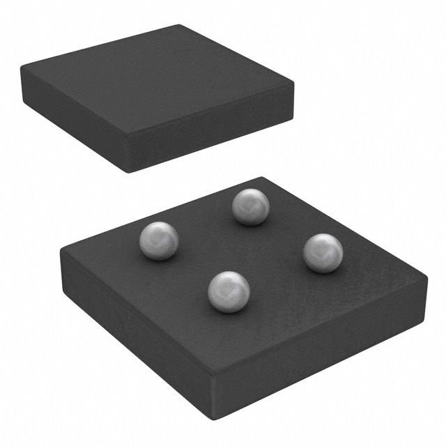
Small form factor
Low power consumption
- Low energy 4-byte write: 200nJ
- Active write: 1.0 mA
- Active read current: 0.2 mA
- Typical standby current: 15 µA
Fast write
- 4-byte write: 40 µs
- 32-byte page write: 0.3 ms
Flexible byte and page write modes: 1 to 32 bytes
Random and sequential read modes
0.75 mm
128-byte one-time programmable (OTP)
security register
A
B
- 64 bytes factory programmed with
unique identifier
1
Vcc
GND
- 64 bytes user programmable
0.75 mm
Software write protect
- All, ½, or ¼ of the array can be protected
2
SCL
SDA
2-wire I2C interface
- 100 kHz
- 400 kHz
0.40 mm
- 1 MHz
RoHS-compliant and halogen-free packaging
Data retention: 10 years
Endurance: 10,000 write cycles
Unlimited read cycles
Packaging
- 4-ball WLCSP
- DWF - Die in Wafer Form
0.40 mm
DS-RM24C64AF–137G–03/2019
�Block Diagram
Figure 1-1. Block Diagram
I/O Buffers and Data
Latches
VCC
SCL
SDA
I/O
Control
Logic
Page Buffer
Y-Decoder
Memory
Control
Logic
GND
Address
Latch
&
Counter
X-Decoder
1.
64 Kb
Resistive Memory
RM24C64AF
DS-RM24C64AF–137G–03/2019
2
�2.
Pin Descriptions
Table 2-1.
Symbol
GND
SDA
Pin Descriptions
Pin #
B1
B2
Name/Function
Description
Ground
Ground pin.
Serial Data
Bidirectional pin used to transfer addresses and data into and data
out of the device. It is an open-drain terminal, and therefore
requires a pull-up resistor to VCC. Typical pull-up resistors are:
10KΩ for 100KHz, and 2KΩ for 400KHz and 1MHz.
For normal data transfer, SDA is allowed to change only during SCL
low. Changes during SCL high are reserved for indicating the
START and STOP conditions.
SCL
A2
Serial Clock
This input is used to synchronize the data transfer from and to the
device. SCL is an input only, since it is a slave-only device.
Vcc
A1
Power
Power supply pin
2.1
Pin Out Diagram
2.1.1
Pinouts
WLCSP (Top View, balls not visible)
0.75 mm
1
A
B
Vcc
GND
0.75 mm
0.40 mm
2
SCL
SDA
0.40 mm
RM24C64AF
DS-RM24C64AF–137G–03/2019
3
�3.
I2C Bus Protocol
The I2C bus is a 2-wire serial bus architecture with a clock pin (SCL) for synchronization, and a data pin (SDA) for data
transfer. The SDA data pin is bi-directional. The SCL clock pin is an input only because the device is slave-only. The SCL
and SDA pins are both externally connected to a positive supply voltage via a current source or pull-up resistor. When
the bus is free, both lines are high. The output stages of devices connected to the bus must have an open drain or open
collector to perform a wired-AND function. Data on the I2C bus can be transferred at rates of up to 1 Mbit/s. The number
of interfaces that may be connected to the bus is solely dependent on the bus capacitance limit of 400pF.
The data on the SDA line must be stable during the high period of the clock. The high or low state of the data line can
only change when the clock signal on the SCL line is low (see Figure 3-1).
Figure 3-1. Bit Transfer on the I2C bus
A high-to-low transition on the SDA line while SCL is high indicates a START condition. A low-to-high transition on the
SDA line while SCL is high defines a STOP condition.
START and STOP conditions are always generated by the master. The bus is considered to be busy after the START
condition. The bus is considered to be free again a certain time after the STOP condition (see Figure 3-2).
Figure 3-2. START and STOP conditions
Every byte put on the SDA line must be 8 bits long. The number of bytes that can be transmitted per transfer is
unrestricted. Each byte must be followed by an acknowledge bit; therefore, the number of clock cycles to transfer one
byte is nine. Data is transferred with the most significant bit (MSB) first.
RM24C64AF
DS-RM24C64AF–137G–03/2019
4
�3.1
I2C Master and Slave Configuration
The RM24C64AF has a two-pin industry-standard I2C interface. It is configured as a slave-only device and therefore
does not generate a clock. 8-pin I2C devices are usually assigned an address by connecting the external E0, E1 and E2
enable pins in the configuration shown in Figure 3-3. This allows up to eight devices can be connected onto an I2C
Interface bus controlled by an I2C master device, such as a micro-controller. The RM24C64AF lacks the external enable
pins, but comes in two predefined configurations, RM24C64AF-0 and RM24C64AF-7, which allows it to take the position
as Memory Device #0 or Memory Device #7 on the I2C bus.
Figure 3-3. Connection between I2C Master and Slaves
I2C Master
(Microcontroller)
RM24C64AF-7
SCL
I2C
Interface
VCC VCC
VCC
E2 E1 E0
I2C
Memory
Device #6
E2 E1 E0
I2C
Memory
Device #5
SDA
SCL
SDA
I2C
Memory
Device #3
SCL
SDA
SCL
SDA
I2C
Memory
Device #2
SCL
VCC
VCC
E2 E1 E0
I2C
Memory
Device #4
SDA
SCL
SDA
SDA
I2C
Memory
Device #1
SCL
SDA
SDA
SCL
SCL
E2 E1 E0
VCC VCC
E2 E1 E0
VCC
4.
Device Timing
4.1
Power-Up/Power-Down Voltage and Timing Requirements
RM24C64AF-0
E2 E1 E0
VCC
As the device initializes, there is a transient current demand. While the device is being powered-up, the internal PowerOn-Reset (POR) circuitry keeps the device in a reset mode until the supply voltage rises above the minimum VCC. During
this time, all operations are disabled and the device does not respond to any commands.
The first operation to the device after power-up cannot be started until the supply voltage reaches the minimum VCC level
and an internal device delay has elapsed. This delay is a maximum time of tPUD. After the tPUD time, the device enters
standby mode. For the case of power-down then power-up operation, or if a power interruption occurs, the VCC of the
device must be maintained below VPWD for at least the minimum specified TPWD time. This is to ensure the device resets
properly after a power interruption.
Table 4-1.
Symbol
Voltage and Timing Requirements for Power-Up / Power-Down
Parameter
Min
Max
10
Units
tPWD
Minimum low time during brown-out.
ms
VPWD
Maximum voltage during brown-out.
0.2
V
tVR
VCC rise time.
200
ms
tPUD
Power-up device delay before access is allowed.
250
µs
RM24C64AF
DS-RM24C64AF–137G–03/2019
5
�Figure 4-1. Bus Timing Data
tFL
tSCLL
tSCLH
tRI
SCL
tSTS
SDA In
tDAH
tSTH
tDAS
tSTPS
tSP
tOV
tBFT
SDA Out
Figure 4-2. Power-Up Timing
VCC
VCC min
tPUD
Full Operation Permitted
Max VPWD
tPWD
tVR
Time
5.
Device Addressing
The first byte sent from the master device to the EEPROM following the START condition is the control byte (See Figure
5-1). The first four bits of the control byte indicate the control code. When accessing the EEPROM memory area, the
control code is “1010” both for read and for write operations. When accessing the OTP Security Registers, the control
code is “1011” both for read and for write operations.
The next three bits of the control byte are the enable bits (E2, E1 and E0), which are “000” for an RM24C64AF-0 device
and “111” for an RM24C64AF-7 device. The E0, E1 and E2 bits sent in the control byte must correspond to the internal
E0, E1 and E2 bits for a device to be selected. In effect, the E0, E1 and E2 bits in the control register act as the three
MSB bits of a word address. These three bits allow the use of up to eight I2C devices on the same bus, of which one can
be an RM24C64AF-0 device and one can be an RM24C64AF-7 device. The last bit of the control byte (R/W) defines the
RM24C64AF
DS-RM24C64AF–137G–03/2019
6
�operation to be performed, read or write. If set to a logic one, a read operation is selected. If set to a logic zero, a write
operation is selected.
Figure 5-1. Control Byte, EEPROM Access
Figure 5-2. Control Byte, OTP Security Register and WP Register Access
Upon receiving the correct control code, the chip enable bits, and the R/W bit, the device performs an acknowledge by
pulling the SDA line low during the 9th clock pulse. As stated above, the device is now set for either a read or a write
operation by the R/W bit.
After the device acknowledges the control byte, two additional bytes are sent by the master to the slave. These bytes
define the target address of the byte in the device to be written. The bit assignment for the address is shown in
Figure 5-3. It should be noted that not all the address bits are used. For the RM24C64AF, only address A0 to A12 are
used; the rest are don't cares and must be set to “0”.
Figure 5-3. Address Sequence Bit Assignments
The device acknowledges each byte of data that is received by pulling the SDA line low during the 9th clock pulse. If the
device does not provide an acknowledge, it has not received the data, in which case the entire sequence, starting with
the control byte, must be resent.
RM24C64AF
DS-RM24C64AF–137G–03/2019
7
�6.
Byte Write Operation
If the R/W bit in the control byte is set to zero, the device enters write mode, where the following sequence of events
occurs.
Once the control byte is received, the device sends an acknowledge. It is then ready to receive the address high byte
(see Figure 6-1).
After receiving the address high byte, the device sends an acknowledge and is ready to receive the address low byte.
After receiving the address low byte, the device acknowledges and then writes the address (expressed by the high and
low address bytes) into its address pointer.
The device is then ready to receive a byte of data to be written into the addressed memory location.
After the device receives the data, it performs an acknowledge.
After the master has received the last acknowledge (after the data byte) the master should send a STOP condition.
The STOP condition initiates the internal write cycle in the device. If the master does not send a STOP, the device does
not write the data into the addressed memory location.
While the device is in the write cycle it will not generate an acknowledge signal. Meanwhile, the master can poll the
device to determine when the write cycle is complete by sending it a control byte and looking for an acknowledge. Once
the write cycle has completed, the device acknowledges the control byte sent to it.
If the byte written is the last byte in a 32-byte page, the address wraps around to the beginning of the same page. For
instance, if the byte is written to address 01FFh, the incremented address will be 01E0h. If the byte is written to address
073Fh, the incremented address will be 0720h.
Note that even though the device supports single byte operation, it operates internally on 4-byte words. The write time for
a single byte is therefore the same as for a 4-byte word.
Figure 6-1. Byte Write Cycle
7.
Page Write Operation
Table 7-1.
Density and Page Size
Product
Density
Page Size (byte)
RM24C64AF
64 Kbit
32
During a page write cycle, a page with up to 32 bytes of data can be written in one continuous write command. The page
write starts in the same manner as the byte write. In a page write, after the acknowledge following the first data byte, the
master does not send a STOP, but continues to send additional data bytes (see Figure 7-1). At the end of the number of
bytes to be written, the master sends a STOP command. Once the STOP command is sent, the device writes all the data
bytes into memory, starting at the address location given in the address bytes.
If the master should transmit more than 32 bytes prior to generating the STOP command, the internal 32-byte data buffer
in the device wraps around and the first data bytes transmitted are overwritten.
RM24C64AF
DS-RM24C64AF–137G–03/2019
8
�The internal address pointer is not increment beyond a page boundary but instead wraps around to the first byte of the
addressed page.
As with the byte write cycle, once the STOP command is received the device enters a write cycle. During the write cycle,
the device does not generate an acknowledge signal. Meanwhile, the master can poll the device to determine when the
write cycle is complete by sending it a control byte and looking for an acknowledge. Once the write cycle has completed,
the device acknowledges the control byte sent to it.
During the page write cycle, the first byte in the data byte buffer is written in the address location indicated by the address
bytes transmitted to the device. Each successive data byte is written in successive address locations.
Note that the page write operation is internally executed by sequentially writing the words in the page buffer. Therefore
the page write time can be estimated as byte write time multiplied by the number of words to be written.
Figure 7-1. Page Write Cycle Bus Transfer
Figure 7-2. Page Write Cycle Timing
SCL
SDA
8th Bit
ACK
WORDN
t PW
Stop
Condition
8.
Start
Condition
Write Protection
The RM24C64 has a software write protect feature which prevents accidental writes. By writing specific values in register
located addresses (see below) the memory array can be write-protected in blocks (as follows):
Top quarter of memory array
Top half of memory array
All of memory array
Write Protection Register (only bits 3/2 are implemented), these two bits are non-volatile
The bits 3/2 are named BP1 and BP0 and provide the protection for the memory and allow part or the whole
memory area to be write protected
Read/Write to the WP register is done using the “1011” command with address A[15:0] = 16'h0401
RM24C64AF
DS-RM24C64AF–137G–03/2019
9
�Table 8-1.
BP1:BP0 Encoding of 64K Device
BP1
BP0
Protected Region
Protected Address (128
kbit)
Protected Area Size (128
kbit)
0
0
None
None
0
0
1
Top 1/4
1800 - 1FFF
2 kBytes
1
0
Top 1/2
1000 - 1FFF
4 kBytes
1
1
All
0 - 1FFF
All
The Adesto RM24C64AF uses a 1-byte Write Protect (WP) Register. The non-volatile bits BP1 and BP0 are found in the
WP Register. The WP Register format is shown in Table 8-2. The WP Register bit definitions are shown in Table 8-3.
Note: The first time a new device is programmed, the non-volatile Block Protection bits (BP0 and BP1) should be written
to 0 before writing data to the EEPROM memory.
Table 8-2.
Write Protect Register Format
Bit7
Bit6
Bit5
Bit4
Bit3
Bit2
Bit1
Bit0
0
0
0
0
BP1
BP0
0
0
Table 8-3.
Bit
Write Protect Bit Definitions
Name
Description
R/W
Non-Volatile Bit
0
N/A
Reserved. Read as “0”
N/A
No
1
N/A
Reserved. Read as “0”
N/A
No
2
BP0
R/W
Yes
3
BP1
Block Protection Bits. “0” indicates the specific blocks are not protected.
“1” indicates that the specific blocks are protected.
4
N/A
Reserved. Read as “0”
N/A
No
5
N/A
Reserved. Read as “0”
N/A
No
6
N/A
Reserved. Read as “0”
N/A
No
7
N/A
Reserved. Read as “0”
N/A
No
The Write Protect (WP) register write operation is similar to the byte write operation, except that the control code (the first
four bits of the command byte) is “1011” instead of “1010”. The address of the WP register is 0401h.
If the R/W bit in the control byte is set to zero, the device enters write mode and the following events occur.
Once the control byte is received, the device performs an acknowledge. It is then ready to receive the address high
byte, 04h (see Figure 8-1).
After receiving the address high byte, the device acknowledges and is ready to receive the address low byte, 01h.
After receiving the address low byte, the device acknowledges and then writes the address (0401h) into its address
pointer. The device is then ready to receive a byte of data to be written into the WP Register.
After the device receives the data, it performs an acknowledge.
After the master has received the last acknowledge (after the data byte), the master should send a STOP condition.
The STOP condition initiates the internal write cycle in the device. If the master does not send a STOP, the device does
not write the data into the WP Register.
RM24C64AF
DS-RM24C64AF–137G–03/2019
10
�Figure 8-1. Write Protect Register Write Cycle
9.
Maximize Bus Throughput by Write Cycle Polling using ACK
The fact that the device does not acknowledge during a write cycle can be used to determine when the write cycle is
complete. By polling the device during the write cycle, bus throughput can be maximized.
Once the STOP command for the write cycle is sent by the master, the device initiates the internally timed write cycle.
Acknowledge polling, by the master, can be initiated immediately. Acknowledge polling involves the master sending a
START command, followed by the control byte for a write command (R/W = 0). If the device is still busy with the write
cycle, no acknowledge is returned. If no acknowledge is returned, the START command and control byte can be retransmitted. If the write cycle is complete, the device returns an acknowledge. The master can then proceed with the next
read or write command. See for a flow diagram.
NOTE: Care must be taken when polling the device. The control byte that was used to initiate the write must match the
control byte used for polling.
Figure 9-1. Write Cycle Polling Flow Using ACK
RM24C64AF
DS-RM24C64AF–137G–03/2019
11
�10.
OTP Security Register Write Operation
The RM24C64AF device contains a specialized OTP security register that can be used for purposes such as unique
device serialization or locked key storage. The OTP register is organized as follows:
The register is comprised of a total of 128 bytes divided into two portions.
The first 64 bytes (byte locations 0 through 63) are allocated as an One-Time Programmable space.
The first 63 bytes (byte locations 0 through 62) can be programmed (but not erased) in any order as long as byte 63 is
not programmed.
Once byte 63 is programmed to any value (including 0xFF), the OTP register is locked, and no further programming
operations are allowed.
The remaining 64 bytes of the register (byte locations 64 through 127) are factory programmed by Adesto and contains
a unique value for each device. The factory programmed data is fixed and cannot be changed.
Table 10-1. OTP Security Register
Security Register Byte Number
0
Data Type
1
···
One-Time User Programmable
63
64
65
···
127
Factory Programmed by Adesto
The OTP security register write operation is similar to the page write operation, except that the control code (the first four
bits of the command byte) is “1011” instead of “1010”.
During a security register write cycle, a page with up to 64 bytes of data can be written in one continuous write command.
The security register write starts in the same manner as the byte write. in a security register write, after the acknowledge
following the first data byte, the master does not send a STOP, but continues to send additional data bytes. (See Figure
10-1.) At the end of the number of bytes to be written, the master sends a STOP command. Once the STOP command is
sent, the device writes all the data bytes into memory, starting at the address location given in the address bytes.
Note that the lower 6 bits of the address are considered by the OTP Security register write operation. Address bit A6
must be set to 0 to write to the OTP security register. The upper 9 bits must be 0. Any attempt to write to address 128, for
instance, is ignored.
If the master should transmit more than 64 bytes prior to generating the STOP command, the internal 64-byte data buffer
in the device will wrap around and the first data bytes transmitted will be overwritten.
The internal address pointer does not increment beyond a page boundary but instead wraps around to the first byte of
the OTP security register.
As with the byte write cycle, once the STOP command is received the device enters a write cycle. During the write cycle,
the device does not generate an acknowledge signal. Meanwhile, the master can poll the device to determine when the
write cycle is complete by sending it a control byte and looking for an acknowledge. Once the write cycle has completed,
the device acknowledges the control byte sent to it.
During the OTP security register write cycle, the first byte in the data byte buffer is written to the address location
indicated by the address bytes transmitted to the device. Each successive data byte is written to successive address
locations.
Note that the OTP security register write operation is internally executed by sequentially writing the words in the page
buffer. Therefore, the OTP security register write time can be estimated as byte write time multiplied by the number of
words to be written.
Note that each byte in the OTP security register can only be written once. Care should be taken to avoid writing to
already written locations. The result of writing to the same location more than once is undefined.
RM24C64AF
DS-RM24C64AF–137G–03/2019
12
�Figure 10-1. OTP Security Register Write Cycle
11.
Read Operation
Read operations are initiated in the same way as the write operations, except that the R/W bit of the control byte is set to
one. There are three types of read operations: current address read, random read, and sequential read.
Note that the same address pointer is used for accessing both the EEPROM array and the OTP security registers.
Changes done to the address register as a result of access to one of the arrays affect the access of the other unless the
address pointer gets updated again.
11.1
Current Address Read
The device internal address pointer maintains the address of the last word accessed, internally incremented by one.
Therefore, if the previous read access was to address n (any legal address), the next current address read operation
would access data from address n+1. After the last memory address, the address counter “rolls-over”, and the device
continues to output data from memory address 00h.
If a current address read is performed after a byte write or page write, care must be taken to understand that during the
page/byte write command, the address can wrap around within the same page.
Upon receipt of the control byte with the R/W bit set to one, the device issues an acknowledge and transmits the 8-bit
data word located at the address of the internal address pointer. The master does not acknowledge the transfer, but does
generate a STOP condition and the device discontinues transmission. See Figure 11-1.
Figure 11-1. Current Address Read
11.2
Random Read
Random read operations allow the master to access any memory location in a random manner. To perform a Random
Read, first the address to be accessed must be set. This is done by sending the address to the device as part of a write
operation (R/W = 0). After the address is sent and acknowledged by the device, the master generates a START. This
terminates the write operation, but the address pointer is set to the address sent. The master then issues the same
control byte as the write operation, but with the R/W bit set to 1. The device acknowledges and transmits the 8-bit data
byte located at the address location written. The master does not acknowledge the transfer of the data byte, but instead
generates a STOP condition, which causes the device to discontinue transmission. See Figure 11-2. After the random
read operation, the internal address counter increments to the address location following the one that was just read.
RM24C64AF
DS-RM24C64AF–137G–03/2019
13
�Figure 11-2. Random Read
11.3
Sequential Read
A sequential read allows the whole memory contents to be serially read during one operation. A sequential read is
initiated in the same way as a random read except that after the device transmits the first data byte, the master issues an
acknowledge instead of a STOP condition. This acknowledge from the master directs the device to transmit the next
sequentially addressed byte (See Figure 11-3). Following the final byte transmitted to the master, the master does not
generate an acknowledge, but rather generates a STOP condition which causes the device to discontinue transmission.
To provide the sequential read, the device contains an internal address pointer which is incremented by one at each
acknowledge received by the master, and by the STOP condition.
Figure 11-3. Sequential Read
12.
Write Protect Register Read Operation
Write Protect (WP) register read operations are initiated in the same way as the write operations, except that the R/W bit
of the control byte is set to one.
Note that the same address pointer is used for accessing both the EEPROM array, the WP register and the OTP security
registers. Changes done to the address register as a result of access to one of the arrays affect the access of the other
unless the address pointer gets updated again. It is recommended that when the user switches between accessing the
EEPROM array, the WP register or the OTP register, a random read is used to explicitly set the address.
The WP Register Read operations will require the address pointer to be set to 0401h.
12.1
Write Protect Register Current Address Read
The device internal address pointer maintains the address of the last word accessed, internally incremented by one.
Therefore, if the previous read access was to address n (any legal address), the next current address read operation
would access data from address n+1. Upon receipt of the control byte with the R/W bit set to one, the device issues an
acknowledge and transmits the 8-bit data word located at the address of the internal address pointer. The master does
not acknowledge the transfer, but does generate a STOP condition and the device discontinues transmission. See Figure
12-1.
RM24C64AF
DS-RM24C64AF–137G–03/2019
14
�Figure 12-1. Write Protect Register Current Address Read
12.2
Write Protect Register Read
To perform a Write Protect Register Read, first the address to be accessed must be set to 0401h. This is done by
sending the address to the device as part of a write operation (R/W = 0). After the address is sent and acknowledged by
the device, the master generates a START. This terminates the write operation, but the address pointer is set to the
address of the WP Register. The master then issues the same control byte as the write operation, but with the R/W bit set
to 1. The device acknowledges and transmits the 8-bit data byte located at the address location written. The master does
not acknowledge the transfer of the data byte, but instead generates a STOP condition, which causes the device to
discontinue transmission. See Figure 12-2. After the WP register read operation, the internal address counter increments
to the address location following the one that was just read.
Figure 12-2. WP Register Read
13.
OTP Security Register Read Operation
OTP security register read operations are initiated in the same way as the write operations, except that the R/W bit of the
control byte is set to one. There are three types of OTP Security Register Read operations: OTP Security Register
current address read, OTP security register random read, and OTP security register sequential read.
Note that the same address pointer is used for accessing both the EEPROM array, the WP register and the OTP security
registers. Changes done to the address register as a result of access to one of the arrays affect the access of the other
unless the address pointer gets updated again. It is recommended that when the user switches between accessing the
EEPROM array, the WP register or the OTP register, a random read is used to explicitly set the address.
The OTP security register read operations require the upper 9 bits of the address pointer to all be 0, but all bits of the
address pointer are updated by these read operations.
Reading address 0 - 63 provides access to the user programmable section of the OTP security registers, while reading
address 64 - 127 provides access to the registers that are factory programmed by Adesto. See Table l for details.
13.1
OTP Security Register Current Address Read
The device internal address pointer maintains the address of the last word accessed, internally incremented by one.
Therefore, if the previous read access was to address n (any legal address), the next current address read operation
would access data from address n+1. Upon receipt of the control byte with the R/W bit set to one, the device issues an
acknowledge and transmits the 8-bit data word located at the address of the internal address pointer. The master does
not acknowledge the transfer, but does generate a STOP condition and the device discontinues transmission. See Figure
13-1.
RM24C64AF
DS-RM24C64AF–137G–03/2019
15
�Figure 13-1. OTP Security Register Current Address Read
13.2
OTP Security Register Random Read
Random read operations allow the master to access any OTP Security Register location in a random manner. To perform
a OTP Security Register Random Read, first the address to be accessed must be set. This is done by sending the
address to the device as part of a write operation (R/W = 0). After the address is sent and acknowledged by the device,
the master generates a START. This terminates the write operation, but the address pointer is set to the address sent.
The master then issues the same control byte as the write operation, but with the R/W bit set to 1. The device
acknowledges and transmits the 8-bit data byte located at the address location written. The master does not
acknowledge the transfer of the data byte, but instead generates a STOP condition, which causes the device to
discontinue transmission. See Figure 13-2. After the OTP security register random read operation, the internal address
counter increments to the address location following the one that was just read.
Figure 13-2. OTP Security Register Random Read
13.3
OTP Security Register Sequential Read
Sequential read allows the whole OTP security register contents to be serially read during one operation. A sequential
read operation is initiated in the same way as a random read except that after the device transmits the first data byte, the
master issues an acknowledge instead of a STOP condition. This acknowledge from the master directs the device to
transmit the next sequentially addressed byte (See Figure 13-3). Following the final byte transmitted to the master, the
master does not generate an acknowledge, but rather generates a STOP condition which causes the device to
discontinue transmission.
To provide the OTP security register sequential read, the device contains an internal address pointer which is
incremented by one at each acknowledge received by the master, and by the STOP condition.
RM24C64AF
DS-RM24C64AF–137G–03/2019
16
�Figure 13-3. OTP Security Register Sequential Read
14.
Electrical Specifications
14.1
Absolute Maximum Ratings*
Table 14-1.Absolute Maximum Ratings
Parameter
Specification
Operating ambient temp range
-40°C to +85°C
Storage temperature range
-65°C to +125°C
Input supply voltage, VCC to GND
Voltage on any pin with respect to GND
ESD protection on all pins (Human Body Model)
- 0.5V to 2.7V
-0.5V to (VCC + 0.5V)
>2kV
*NOTICE: Stresses beyond those listed under “Absolute Maximum Ratings” may cause permanent damage to the
device. This is a stress rating only and functional operation of the device at these, or any other conditions beyond those
indicated in the operational sections of this specification, is not implied. Exposure to absolute maximum rating conditions
for extended periods may affect device reliability.
RM24C64AF
DS-RM24C64AF–137G–03/2019
17
�14.2
DC Characteristics
Table 14-2. DC Characteristics (1)
Condition
Symbol
Parameter
TA = -40°C to +85° C, VCC = 1.65V to 2.2V
Min
VCC
Supply range
1.65V to 2.2V
1.65
ICC1
Supply current, read
VCC = 2.2V SCL at 1MHz
ICC2
Supply current, write
ICC3
Max
Units
2.2
V
0.2
0.5
mA
VCC = 2.2V
1.0
2
mA
Supply current, standby (2)
VCC = 2.2V. SCL = SDA = 2.2V
15
35
µA
IIL
Input leakage
SCL, SDA, VIN = 0V or VCC
+1
µA
IOL
Output leakage
SDA VIN = 0V to VCC
+1
µA
VIL
Input low voltage
SCL, SDA
-0.5
VCC x 0.3
V
VIH
Input high voltage
SCL, SDA
VCC x 0.7
VCC + 0.5
V
VOL
Output low voltage
SDA IOL = 300 µA
0.2
V
1.
Applicable over the recommended operating range: TA = -40°C to +85 °C, VCC = 1.65V to 2.2V, CL = CB < 100pF
2.
Values are based on device characterization, not 100% tested in production.
Typ
RM24C64AF
DS-RM24C64AF–137G–03/2019
18
�14.3
AC Characteristics
Applicable over recommended operating range: TA = -40°C to +85° C, VCC = 1.65V to 2.2V, CL = CB