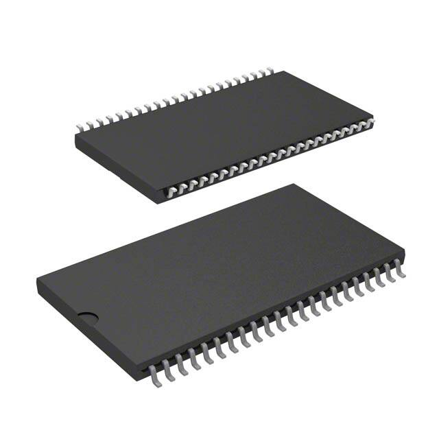
RMLV0808BGSB-4S2#AA0 数据手册
RMLV0808BGSB - 4S2
8Mb Advanced LPSRAM (1024k word × 8bit)
R10DS0232EJ0201
Rev.2.01
2020.02.20
Description
The RMLV0808BGSB is a family of 8-Mbit static RAMs organized 1,048,576-word × 8-bit, fabricated by Renesas’s
high-performance Advanced LPSRAM technologies. The RMLV0808BGSB has realized higher density, higher
performance and low power consumption. The RMLV0808BGSB offers low power standby power dissipation;
therefore, it is suitable for battery backup systems. It is offered in 44pin TSOP (II).
Features
Single 3V supply: 2.4V to 3.6V
Access time:
── Power supply voltage from 2.7V to 3.6V: 45ns (max.)
── Power supply voltage from 2.4V to 2.7V: 55ns (max.)
Current consumption:
── Standby: 0.45µA (typ.)
Equal access and cycle times
Common data input and output
── Three state output
Directly TTL compatible
── All inputs and outputs
Battery backup operation
Part Name Information
Part Name
Power supply
Access time
2.7V to 3.6V
45 ns
2.4V to 2.7V
55 ns
RMLV0808BGSB-4S2
R10DS0232EJ0201 Rev.2.01
2020.02.20
Temperature
Range
Package
-40 ~ +85°C
11.76mm×18.41mm 44pin plastic TSOP(II)
Page 1 of 11
�RMLV0808BGSB - 4S2
Pin Arrangement
44pin TSOP(II)
A4
1
44
A5
A3
2
43
A6
A2
3
42
A7
A1
4
41
OE#
A0
5
40
CS2
CS1#
6
39
A8
NC
7
38
NC
NC
8
37
NC
DQ0
9
36
DQ7
DQ1
10
35
DQ6
Vcc
11
34
Vss
Vss
12
33
Vcc
DQ2
13
32
DQ5
DQ3
14
31
DQ4
NC
15
30
NC
NC
16
29
NC
WE#
17
28
A9
A19
18
27
A10
A18
19
26
A11
A17
20
25
A12
A16
21
24
A13
A15
22
23
A14
(Top view)
Pin Description
Pin name
Function
VCC
VSS
A0 to A19
DQ0 to DQ7
CS1#
CS2
OE#
Ground
Address input
Data input/output
Chip select 1
Chip select 2
Output enable
Power supply
WE#
NC
Write enable
No connection
R10DS0232EJ0201 Rev.2.01
2020.02.20
Page 2 of 11
�RMLV0808BGSB - 4S2
Block Diagram
A0
A1
ADDRESS
ROW
MEMORY ARRAY
BUFFER
DECODER
1024k-word x8-bit
A19
DQ0
DQ
BUFFER
DQ1
SENSE / WRITE AMPLIFIER
DQ7
COLUMN DECODER
CLOCK
GENERATOR
Vcc
WE#
Vss
CS1#
CS2
OE#
Operation Table
CS1#
CS2
WE#
OE#
DQ0~7
Operation
H
X
X
X
High-Z
Stand-by
X
L
X
X
High-Z
Stand-by
L
H
L
X
Din
Write
L
H
H
L
Dout
Read
L
H
H
H
High-Z
Output disable
Note 1.
H: VIH L:VIL
X: VIH or VIL
R10DS0232EJ0201 Rev.2.01
2020.02.20
Page 3 of 11
�RMLV0808BGSB - 4S2
Absolute Maximum Ratings
Parameter
Symbol
Power supply voltage relative to VSS
VCC
Terminal voltage on any pin relative to VSS
VT
Power dissipation
PT
Operation temperature
Topr
Storage temperature range
Tstg
Storage temperature range under bias
Tbias
Note 2. -3.0V for pulse ≤ 30ns (full width at half maximum)
3. Maximum voltage is +4.6V.
Value
-0.5 to +4.6
-0.5*2 to VCC+0.3*3
0.7
-40 to +85
-65 to +150
-40 to +85
unit
V
V
W
°C
°C
°C
DC Operating Conditions
Parameter
Supply voltage
Symbol
VCC
VSS
Input high voltage
VIH
Input low voltage
VIL
Min.
2.4
0
Typ.
3.0
0
─
Max.
3.6
0
VCC+0.2
Unit
V
V
V
2.0
2.2
Test conditions
Note
Vcc=2.4V to 2.7V
─
VCC+0.2
V
Vcc=2.7V to 3.6V
-0.2
─
0.4
V
Vcc=2.4V to 2.7V
4
-0.2
─
0.6
V
Vcc=2.7V to 3.6V
4
Ambient temperature range
Ta
-40
─
Note 4. -3.0V for pulse ≤ 30ns (full width at half maximum)
+85
°C
DC Characteristics
Parameter
Input leakage current
Output leakage current
Symbol
| ILI |
Min.
─
Typ.
─
Max.
1
Unit
A
| ILO |
─
─
1
A
─
20*5
25
mA
─
25*5
30
mA
ICC2
─
1.5*5
3
mA
ISB
─
─
0.3
mA
CS2 = VIL, Others = VSS to VCC
─
0.45*5
2
A
~+25°C
─
0.6*6
4
A
~+40°C
─
─
7
A
~+70°C
─
─
10
A
~+85°C
VOH
2.4
─
─
V
VOH2
2.0
─
─
V
VOL
─
─
0.4
V
Average operating current
ICC1
Standby current
Standby current
Test conditions
Vin = VSS to VCC
CS1# = VIH or CS2 = VIL or OE# = VIH
or WE# = VIL , VI/O = VSS to VCC
Cycle = 55ns, duty =100%, II/O = 0mA,
CS1# = VIL, CS2 = VIH, Others = VIH/VIL
Cycle = 45ns, duty =100%, II/O = 0mA,
CS1# = VIL, CS2 = VIH, Others = VIH/VIL
Cycle = 1s, duty =100%, II/O = 0mA,
CS1# ≤ 0.2V, CS2 ≥ VCC-0.2V,
VIH ≥ VCC-0.2V, VIL ≤ 0.2V
ISB1
Output high voltage
Output low voltage
Note
Note
Vin = VSS to VCC,
(1) CS2 ≤ 0.2V or
(2) CS1# ≥ VCC-0.2V,
CS2 ≥ VCC-0.2V
IOH = -1mA
Vcc≥2.7V
IOH = -0.1mA
IOL = 2mA
Vcc≥2.7V
VOL2
─
─
0.4
V
IOL = 0.1mA
5. Typical parameter indicates the value for the center of distribution at 3.0V (Ta=25ºC), and not 100% tested.
6. Typical parameter indicates the value for the center of distribution at 3.0V (Ta=40ºC), and not 100% tested.
R10DS0232EJ0201 Rev.2.01
2020.02.20
Page 4 of 11
�RMLV0808BGSB - 4S2
Capacitance
(Ta =25°C, f =1MHz)
Parameter
Symbol
Min.
Input capacitance
C in
─
Input / output capacitance
C I/O
─
Note 7. This parameter is sampled and not 100% tested.
Typ.
─
─
Max.
8
10
Unit
pF
pF
Test conditions
Vin =0V
VI/O =0V
Note
7
7
AC Characteristics
Test Conditions (Vcc = 2.4V ~ 3.6V, Ta = -40 ~ +85°C)
1.4V
Input pulse levels:
VIL = 0.4V, VIH = 2.4V (Vcc=2.7V to 3.6V)
VIL = 0.4V, VIH = 2.2V (Vcc=2.4V to 2.7V)
Input rise and fall time: 5ns
Input and output timing reference level: 1.4V
Output load: See figures (Including scope and jig)
RL = 500 ohm
DQ
CL = 30 pF
Read Cycle
Parameter
Vcc=2.7V to 3.6V
Vcc=2.4V to 2.7V
Unit
Note
Min.
Max.
Min.
Max.
Read cycle time
tRC
45
─
55
─
ns
Address access time
tAA
─
45
─
55
ns
tACS1
─
45
─
55
ns
Chip select access time
tACS2
─
45
─
55
ns
Output enable to output valid
tOE
─
22
─
30
ns
Output hold from address change
tOH
10
─
10
─
ns
tCLZ1
10
─
10
─
ns
8,9
Chip select to output in low-Z
tCLZ2
10
─
10
─
ns
8,9
Output enable to output in low-Z
tOLZ
5
─
5
─
ns
8,9
tCHZ1
0
18
0
20
ns
8,9,10
Chip deselect to output in high-Z
tCHZ2
0
18
0
20
ns
8,9,10
Output disable to output in high-Z
tOHZ
0
18
0
20
ns
8,9,10
Note 8. This parameter is sampled and not 100% tested.
9. At any given temperature and voltage condition, tCHZ1 max is less than tCLZ1 min, tCHZ2 max is less than tCLZ2
min, and tOHZ max is less than tOLZ min, for any device.
10. tCHZ1, tCHZ2 and tOHZ are defined as the time when the DQ pins enter a high-impedance state and are not
referred to the DQ levels.
R10DS0232EJ0201 Rev.2.01
2020.02.20
Symbol
Page 5 of 11
�RMLV0808BGSB - 4S2
Write Cycle
Parameter
Symbol
Vcc=2.7V to 3.6V
Vcc=2.4V to 2.7V
Min.
Max.
Min.
Max.
Write cycle time
tWC
45
─
55
─
Address valid to write end
tAW
35
─
50
─
Chip select to write end
tCW
35
─
50
─
Write pulse width
tWP
35
─
40
─
Address setup time to write start
tAS
0
─
0
─
Write recovery time from write end
tWR
0
─
0
─
Data to write time overlap
tDW
25
─
25
─
Data hold from write end
tDH
0
─
0
─
Output enable from write end
tOW
5
─
5
─
Output disable to output in high-Z
tOHZ
0
18
0
20
Write to output in high-Z
tWHZ
0
18
0
20
Note 11. tWP is the interval between write start and write end.
A write starts when all of (CS1#), (WE#) and (CS2) become active.
A write is performed during the overlap of a low CS1#, a low WE# and a high CS2.
A write ends when any of (CS1#), (WE#) or (CS2) becomes inactive.
12. This parameter is sampled and not 100% tested.
13. tOHZ and tWHZ are defined as the time when the DQ pins enter a high-impedance state and
the DQ levels.
R10DS0232EJ0201 Rev.2.01
2020.02.20
Unit
ns
ns
ns
ns
ns
ns
ns
ns
ns
ns
ns
Note
11
12
12,13
12,13
are not referred to
Page 6 of 11
�RMLV0808BGSB - 4S2
Timing Waveforms
Read Cycle
tRC
Valid address
A0~19
tAA
tACS1
CS1#
CS2
WE#
tCLZ1 *15,16
tCHZ1 *14,15,16
tACS2
tCLZ2 *15,16
tCHZ2 *14,15,16
VIH
WE# = “H” level
tOHZ *14,15,16
tOE
OE#
tOLZ
DQ0~7
High impedance
tOH
*15,16
Valid Data
Note 14. tCHZ1, tCHZ2 and tOHZ are defined as the time when the DQ pins enter a high-impedance state and are not
referred to the DQ levels.
15. This parameter is sampled and not 100% tested
16. At any given temperature and voltage condition, tCHZ1 max is less than tCLZ1 min, tCHZ2 max is less than tCLZ2
min, and tOHZ max is less than tOLZ min, for any device.
R10DS0232EJ0201 Rev.2.01
2020.02.20
Page 7 of 11
�RMLV0808BGSB - 4S2
Write Cycle (1) (WE# CLOCK, OE#=”H” while writing)
tWC
Valid address
A0~19
tCW
CS1#
CS2
tCW
tWR
tAW
tWP *17
WE#
tAS
OE#
tWHZ *18,19
tOHZ *18,19
DQ0~7
*20
tDW
tDH
Valid Data
Note 17. tWP is the interval between write start and write end.
A write starts when all of (CS1#), (WE#) and (CS2) become active.
A write is performed during the overlap of a low CS1#, a low WE# and a high CS2.
A write ends when any of (CS1#), (WE#) or (CS2) becomes inactive.
18. tOHZ and tWHZ are defined as the time when the DQ pins enter a high-impedance state and are not referred to
the DQ levels.
19. This parameter is sampled and not 100% tested
20. During this period, DQ pins are in the output state so input signals must not be applied to the DQ pins.
R10DS0232EJ0201 Rev.2.01
2020.02.20
Page 8 of 11
�RMLV0808BGSB - 4S2
Write Cycle (2) (WE# CLOCK, OE# Low Fixed)
tWC
Valid address
A0~19
tCW
CS1#
CS2
tCW
tAW
tWR
tWP *21
WE#
OE#
OE# = “L” level
tAS
VIL
tWHZ *22,23
DQ0~7
*24
tOW
Valid Data
tDW
*24
tDH
Note 21. tWP is the interval between write start and write end.
A write starts when all of (CS1#), (WE#) and (CS2) become active.
A write is performed during the overlap of a low CS1#, a low WE# and a high CS2.
A write ends when any of (CS1#), (WE#) or (CS2) becomes inactive.
22. tWHZ is defined as the time when the DQ pins enter a high-impedance state and are not referred to the DQ
levels.
23. This parameter is sampled and not 100% tested.
24. During this period, DQ pins are in the output state so input signals must not be applied to the DQ pins.
R10DS0232EJ0201 Rev.2.01
2020.02.20
Page 9 of 11
�RMLV0808BGSB - 4S2
Write Cycle (3) (CS1#, CS2 CLOCK)
tWC
Valid address
A0~19
tAW
tAS
tCW
tAS
tCW
tWR
CS1#
CS2
tWP *25
WE#
OE#
VIH
OE# = “H” level
tDW
DQ0~7
tDH
Valid
Valid Data
Data
Note 25. tWP is the interval between write start and write end.
A write starts when all of (CS1#), (WE#) and (CS2) become active.
A write is performed during the overlap of a low CS1#, a low WE# and a high CS2.
A write ends when any of (CS1#), (WE#) or (CS2) becomes inactive.
R10DS0232EJ0201 Rev.2.01
2020.02.20
Page 10 of 11
�RMLV0808BGSB - 4S2
Low VCC Data Retention Characteristics
Parameter
Symbol
Min.
Typ.
Max.
Unit
Test conditions*28
VCC for data retention
VDR
1.5
─
3.6
V
Vin ≥ 0V,
(1) CS2 ≤ 0.2V or
(2) CS1# ≥ VCC-0.2V, CS2 ≥ VCC-0.2V
─
0.45*26
2
A
~+25°C
─
0.6*27
4
A
~+40°C
─
─
7
A
~+70°C
─
─
10
A
~+85°C
Data retention current
ICCDR
VCC = 3.0V, Vin ≥ 0V,
(1) CS2 ≤ 0.2V or
(2) CS1# ≥ VCC-0.2V,
CS2 ≥ VCC-0.2V
Chip deselect time to data retention
tCDR
0
─
─
ns
See retention waveform.
Operation recovery time
tR
5
─
─
ms
Note 26. Typical parameter indicates the value for the center of distribution at 3.0V (Ta=25ºC), and not 100% tested.
27. Typical parameter indicates the value for the center of distribution at 3.0V (Ta=40ºC), and not 100% tested.
28. CS2 controls address buffer, WE# buffer, CS1# buffer, OE# buffer and DQ buffer. If CS2 controls data
retention mode, Vin levels (address, WE#, CS1#, OE#, DQ) can be in the high impedance state. If CS1#
controls data retention mode, CS2 must be CS2 ≥ VCC-0.2V or CS2 ≤ 0.2V. The other inputs levels (address,
WE#, OE#, DQ) can be in the high-impedance state.
Low Vcc Data Retention Timing Waveforms (CS1# controlled)
CS1# Controlled
VCC
tCDR
2.4V
2.4V
tR
VDR
2.0V
2.0V
CS1# ≥ VCC - 0.2V
CS1#
Low Vcc Data Retention Timing Waveforms (CS2 controlled)
CS2 Controlled
VCC
tCDR
CS2
0.4V
2.4V
2.4V
VDR
tR
0.4V
CS2 ≤ 0.2V
R10DS0232EJ0201 Rev.2.01
2020.02.20
Page 11 of 11
�Revision History
Rev.
1.00
2.00
Date
2014.11.28
2015.06.26
2.01
2020.02.20
Page
─
P.1, 4
P.2
P.4
P.11
Last page
RMLV0808BGSB Data Sheet
Description
Summary
First Edition issued
Standby current ISB1 : 25°C 0.6µA ->0.45µA (typ.), 40°C 2µA ->0.6µA (typ.)
Modefy Pin Arrangement : Add 1pin Mark
Average operating current ICC2 : 25°C 2mA ->1.5mA (typ.)
Data retention current ICCDR : 25°C 0.6µA ->0.45µA (typ.), 40°C 2µA ->0.6µA (typ.)
Updated the Notice to the latest version
All trademarks and registered trademarks are the property of their respective owners.
�IMPORTANT NOTICE AND DISCLAIMER
RENESAS ELECTRONICS CORPORATION AND ITS SUBSIDIARIES (“RENESAS”) PROVIDES TECHNICAL
SPECIFICATIONS AND RELIABILITY DATA (INCLUDING DATASHEETS), DESIGN RESOURCES (INCLUDING
REFERENCE DESIGNS), APPLICATION OR OTHER DESIGN ADVICE, WEB TOOLS, SAFETY INFORMATION, AND
OTHER RESOURCES “AS IS” AND WITH ALL FAULTS, AND DISCLAIMS ALL WARRANTIES, EXPRESS OR IMPLIED,
INCLUDING, WITHOUT LIMITATION, ANY IMPLIED WARRANTIES OF MERCHANTABILITY, FITNESS FOR A
PARTICULAR PURPOSE, OR NON-INFRINGEMENT OF THIRD PARTY INTELLECTUAL PROPERTY RIGHTS.
These resources are intended for developers skilled in the art designing with Renesas products. You are solely responsible
for (1) selecting the appropriate products for your application, (2) designing, validating, and testing your application, and (3)
ensuring your application meets applicable standards, and any other safety, security, or other requirements. These
resources are subject to change without notice. Renesas grants you permission to use these resources only for
development of an application that uses Renesas products. Other reproduction or use of these resources is strictly
prohibited. No license is granted to any other Renesas intellectual property or to any third party intellectual property.
Renesas disclaims responsibility for, and you will fully indemnify Renesas and its representatives against, any claims,
damages, costs, losses, or liabilities arising out of your use of these resources. Renesas' products are provided only subject
to Renesas' Terms and Conditions of Sale or other applicable terms agreed to in writing. No use of any Renesas resources
expands or otherwise alters any applicable warranties or warranty disclaimers for these products.
(Rev.1.0 Mar 2020)
Corporate Headquarters
Contact Information
TOYOSU FORESIA, 3-2-24 Toyosu,
Koto-ku, Tokyo 135-0061, Japan
www.renesas.com
For further information on a product, technology, the most
up-to-date version of a document, or your nearest sales
office, please visit:
www.renesas.com/contact/
Trademarks
Renesas and the Renesas logo are trademarks of Renesas
Electronics Corporation. All trademarks and registered
trademarks are the property of their respective owners.
© 2020 Renesas Electronics Corporation. All rights reserved.
�