SLG7NT41502
CURIE BASED WEARABLE
LS_ON
Features
Output Summary
• 1 Output — Push Pull 2X
• 1 Output — Open Drain NMOS 1X
• 3 Outputs — Open Drain NMOS 2X
Silego Technology, Inc.
SLG7NT41502_DS_r104
SLG7NT41502_GP_r002
VDD
1
14 13
12
OPM2P6_DISCHARGE
nBUTTON_IN
2
11
nBUTTON_MONITOR
nEXIT_SHIPMODE
3
10
PG_IN
POR_B
4
9
nPG_IN
SHIPMODE_EN
5
8
GND
6
7
DISCHARGE_0
• Low Power Consumption
• Pb-Free / RoHS Compliant
• Halogen-Free
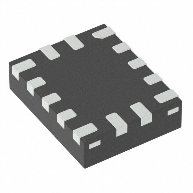
• STQFN-14 Package
DISCHARGE_1
Pin Configuration
Silego SLG7NT41502 is a low power and small
form device. The SoC is housed in a 1.6 x 2.0 mm
STQFN package which is optimal for using with
small devices.
SHIPMODE_STROBE
General Description
STQFN-14
TOP VIEW
Rev 1.04
Revised January 23, 2017
�SLG7NT41502
CURIE BASED WEARABLE
Pin Configuration
Pin #
1
2
3
4
5
6
7
8
9
10
11
12
13
14
Pin Name
VDD
nBUTTON_IN
nEXIT_SHIPMODE
POR_B
SHIPMODE_EN
SHIPMODE_STROBE
DISCHARGE_0
GND
nPG_IN
PG_IN
nBUTTON_MONITOR
OPM2P6_DISCHARGE
DISCHARGE_1
LS_ON
Type
PWR
Digital Input
Digital Input
Digital Input
Digital Input
Digital Input
Digital Output
GND
Digital Input
Digital Input
Digital Output
Digital Output
Digital Output
Digital Output
Pin Description
Supply Voltage
Digital Input with Schmitt trigger
Digital Input with Schmitt trigger
Low Voltage Digital input
Low Voltage Digital input
Low Voltage Digital input
Open Drain NMOS 2X
Ground
Digital Input with Schmitt trigger
Digital Input with Schmitt trigger
Open Drain NMOS 1X
Open Drain NMOS 2X
Open Drain NMOS 2X
Push Pull 2X
Ordering Information
Part Number
SLG7NT41502V
SLG7NT41502VTR
SLG7NT41502_DS_r104
Package Type
V=STQFN-14
STQFN-14 – Tape and Reel (3k units)
Page 2
2
�SLG7NT41502
CURIE BASED WEARABLE
Absolute Maximum Conditions
Parameter
Min.
Max.
Unit
VHIGH to GND
-0.3
7
V
Voltage at input pins
-0.3
7
V
Current at input pin
-1.0
1.0
mA
Storage temperature range
-65
125
°C
Junction temperature
--
150
°C
ESD Protection (Human Body Model)
2000
--
V
ESD Protection (Charged Device Model)
1000
--
V
Moisture Sensitivity Level
1
Electrical Characteristics
(@ 25°C, unless otherwise stated)
Symbol
Parameter
VDD
Supply Voltage
Operating
TA
Temperature
IQ
IA
VO
IO
VIH
Quiescent Current
Active Current
Maximal Voltage
Applied to any PIN in
High-Impedance
State
Maximal Average or
DC Current
(note 1)
HIGH-Level Input
Voltage
(Note 2)
SLG7NT41502_DS_r104
Condition/Note
Static inputs and floating outputs
PIN4 = 1; PIN14 = 1; DFF4 = 0 @VDD = 3.3V
Static inputs and outputs
PIN4 = 0; PIN14 = 0; DFF4 = 1 @VDD = 3.3V
Static inputs and outputs
PIN4 = 1; PIN14 = 1; DFF4 = 0 @VDD = 5.5V
Static inputs and outputs
PIN4 = 0; PIN14 = 0; DFF4 = 1 @VDD = 5.5V
Static outputs
PIN4 = 0; PIN14 = 1; DFF4 = 0 @VDD = 3.7V
Static outputs
PIN4 = 0; PIN14 = 0; DFF4 = 0 @VDD = 3.3V
Static outputs
PIN4 = 0; PIN14 = 1; DFF4 = 0 @VDD = 5.5V
Per Each Chip Side
Logic Input with Schmitt Trigger,
at VDD=1.8V
At temperature -45°C +85°C (note 1)
Low-Level Logic Input, at VDD=1.8V
At temperature -45°C +85°C (note 1)
Logic Input with Schmitt Trigger,
at VDD=3.3V
At temperature -45°C +85°C (note 1)
Min.
1.71
Typ.
3.6
Max.
5.5
Unit
V
-40
25
85
°C
--
1
--
--
1
--
--
1
--
--
1
--
--
50
--
--
1.8
--
--
50
--
--
--
VDD
V
--
--
90
mA
1.27
--
VDD
0.98
--
VDD
2.13
--
VDD
µA
Page 3
3
µA
V
�SLG7NT41502
CURIE BASED WEARABLE
VIL
VHYS
IIH
IIL
VOH
VOL
LOW-Level Input
Voltage
(Note 2)
Schmitt Trigger
Hysteresis Voltage
HIGH-Level Input
Current
LOW-Level Input
Current
HIGH-Level Output
Voltage
(note 1)
LOW-Level Output
Voltage
(note 1)
SLG7NT41502_DS_r104
Low-Level Logic Input, at VDD=3.3V
At temperature -45°C +85°C (note 1)
Logic Input with Schmitt Trigger,
at VDD=5.0V
At temperature -45°C +85°C (note 1)
Low-Level Logic Input, at VDD=5.0V
At temperature -45°C +85°C (note 1)
Logic Input with Schmitt Trigger,
at VDD=1.8V
Low-Level Logic Input, at VDD=1.8V
At temperature -45°C +85°C (note 1)
Logic Input with Schmitt Trigger,
at VDD=3.3V
At temperature -45°C +85°C (note 1)
Low-Level Logic Input, at VDD=3.3V
At temperature -45°C +85°C (note 1)
Logic Input with Schmitt Trigger,
at VDD=5.0V
At temperature -45°C +85°C (note 1)
Low-Level Logic Input, at VDD=5.0V
At temperature -45°C +85°C (note 1)
1.13
--
VDD
3.16
--
VDD
1.23
--
VDD
--
--
0.44
--
--
0.52
--
--
0.95
--
--
0.69
--
--
1.51
--
--
0.78
0.273
--
0.792
V
Logic Input PINs; VIN = VDD
-1.0
--
1.0
µA
Logic Input PINs; VIN = 0V
-1.0
--
1.0
µA
1.679
1.792
--
2.861
3.201
--
4.330
4.878
--
--
0.007
0.010
--
0.007
0.010
--
0.002
0.010
--
0.070
0.130
--
0.079
0.130
Logic Input with Schmitt Trigger
Push Pull,
IOH = 100uA, 2X Driver, at VDD=1.8 V
At temperature -45°C +85°C (note 1)
Push Pull,
IOH = 3mA, 2X Driver, at VDD=3.3 V
At temperature -45°C +85°C (note 1)
Push Pull,
IOH = 5mA, 2X Driver, at VDD=5.0 V
At temperature -45°C +85°C (note 1)
Open Drain,
IOL = 100uA, 1X Driver, at VDD=1.8 V
At temperature -45°C +85°C (note 1)
Push Pull,
IOL = 100uA, 2X Driver, at VDD=1.8 V
At temperature -45°C +85°C (note 1)
Open Drain,
IOL = 100uA, 2X Driver, at VDD=1.8 V
At temperature -45°C +85°C (note 1)
Open Drain,
IOL = 3mA, 1X Driver, at VDD=3.3 V
At temperature -45°C +85°C (note 1)
Push Pull,
IOL = 3mA, 2X Driver, at VDD=3.3 V
At temperature -45°C +85°C (note 1)
V
Page 4
4
V
V
�SLG7NT41502
CURIE BASED WEARABLE
IOH
IOL
HIGH-Level Output
Current
(note 1)
LOW-Level Output
Current
(note 1)
SLG7NT41502_DS_r104
Open Drain,
IOL = 3mA, 2X Driver, at VDD=3.3 V
At temperature -45°C +85°C (note 1)
Open Drain,
IOL = 5mA, 1X Driver, at VDD=5.0 V
At temperature -45°C +85°C (note 1)
Push Pull,
IOL = 5mA, 2X Driver, at VDD=5.0 V
At temperature -45°C +85°C (note 1)
Open Drain,
IOL = 5mA, 2X Driver, at VDD=5.0 V
At temperature -45°C +85°C (note 1)
Push Pull & PMOS OD,
VOH = VDD-0.2, 2X Driver, at VDD=1.8 V
At temperature -45°C +85°C (note 1)
Push Pull & PMOS OD,
VOH = 2.4 V, 2X Driver, at VDD=3.3 V
At temperature -45°C +85°C (note 1)
Push Pull & PMOS OD,
VOH = 2.4 V, 2X Driver, at VDD=5.0 V
At temperature -45°C +85°C (note 1)
Push Pull,
VOL =0.15V, 2X Driver, at VDD=1.8 V
At temperature -45°C +85°C (note 1)
Open Drain,
VOL =0.15V, 1X Driver, at VDD=1.8 V
At temperature -45°C +85°C (note 1)
Open Drain,
VOL =0.15V, 2X Driver, at VDD=1.8 V
At temperature -45°C +85°C (note 1)
Push Pull,
VOL =0.4V, 2X Driver, at VDD=3.3 V
At temperature -45°C +85°C (note 1)
Open Drain,
VOL =0.4V, 1X Driver, at VDD=3.3 V
At temperature -45°C +85°C (note 1)
Open Drain,
VOL =0.4V, 2X Driver, at VDD=3.3 V
At temperature -45°C +85°C (note 1)
--
0.040
0.070
--
0.090
0.160
--
0.101
0.160
--
0.050
0.080
2.069
3.390
--
11.278
21.634
--
40.059
59.691
--
1.52
2.840
--
1.530
2.840
--
3.060
5.680
--
8.130
13.840
--
8.130
13.850
--
mA
mA
16.260
23.700
--
Push Pull,
VOL =0.4V, 2X Driver, at VDD=5.0 V
At temperature -45°C +85°C (note 1)
12.020
19.460
--
Open Drain,
VOL =0.4V, 1X Driver, at VDD=5.0 V
At temperature -45°C +85°C (note 1)
12.030
19.460
--
Open Drain,
VOL =0.4V, 2X Driver, at VDD=5.0 V
At temperature -45°C +85°C (note 1)
24.060
38.920
--
Page 5
5
�SLG7NT41502
CURIE BASED WEARABLE
VACMP0
GACMP0
VHYST
RPULL_UP
RPULL_DOWN
RDIS
TCNT0
Analog Comparator
Threshold Voltage
Analog Comparator0
IN+ gain
Analog Comparator
Hysteresis Voltage
(note 1)
Internal Pull Up
Resistance
Internal Pull Down
Resistance
Discharge
Resistance
Counter0 Period
(WS Ctrl)
TDLY1
Delay1 Time
TDLY2
Delay2 Time
TDLY3
Delay3 Time
TSU
PONTHR
POFFTHR
Start up Time
Power On Threshold
Power Off Threshold
Low to High transition,
at temperature 25°C.
Low to High transition,
at temperature -40 +85°C (note 1)
High to Low transition,
at temperature 25°C
High to Low transition,
at temperature -40 +85°C (note 1)
3532.7
3582.9
3633.1
3519.7
3579.8
3644.2
mV
2948.8
2991.5
3034.2
2937.1
2988.1
3040.9
ACMP 0
--
0.33
--
ACMP 0
--
200
--
mV
Pull up on PIN 2, 3
70
100
130
kΩ
Pull down on PINs 5, 6
70
100
130
kΩ
External resistor on PIN7, PIN12 and PIN13
270
--
--
Ω
At temperature 25°C
At temperature -40°C +85°C (note 1)
At temperature 25°C
At temperature -40°C +85°C (note 1)
At temperature 25°C
At temperature -40°C +85°C (note 1)
At temperature 25°C
At temperature -40°C +85°C (note 1)
From VDD rising past PONTHR
VDD Level Required to Start Up the Chip
VDD Level Required to Switch Off the Chip
153.14
153.14
195.04
184.59
486.52
460.44
195.04
184.59
0.462
0.961
0.875
176.87
178.87
200.45
200.45
500.02
500.02
200.45
200.45
1.4
1.312
1.109
207.44
217.81
206.90
216.47
516.10
539.10
206.90
216.47
4.999
1.659
1.288
1. Guaranteed by Design.
2. No hysteresis for Low Voltage Digital Input
SLG7NT41502_DS_r104
Page 6
6
ms
ms
ms
ms
ms
V
V
�SLG7NT41502
CURIE BASED WEARABLE
Datasheet
Revision
1.04
Programming
Code Number
002
Locked
Status
L
Part Code
Revision
Date
V6
B
01/23/2017
The IC security bit is locked/set for code security for production unless otherwise specified. Revision
number is not changed for bit locking.
SLG7NT41502_DS_r104
Page 7
7
�SLG7NT41502
CURIE BASED WEARABLE
Package Drawing and Dimensions
14 Lead STQFN Package
SLG7NT41502_DS_r104
Page 8
8
�SLG7NT41502
CURIE BASED WEARABLE
Tape and Reel Specification
# of
Package Type
Pins
STQFN 14L
FC 0.4P
Green
14
Max Units
Nominal
Package
Size (mm)
per reel
1.6x2.0x0.55
3000
Trailer A
per box
Reel &
Hub Size
(mm)
Pockets
3000
178/60
100
Leader B
Pocket (mm)
Length
Length
Pockets
(mm)
(mm)
400
100
Width
Pitch
8
4
400
Carrier Tape Drawing and Dimensions
Package
Type
STQFN 14L
FC 0.4P
Green
Pocket
BTM
Length
(mm)
Pocket
BTM Width
(mm)
Pocket
Depth
(mm)
Index Hole
Pitch
(mm)
Pocket
Pitch
(mm)
Index Hole
Diameter
(mm)
Index Hole Index Hole
to Tape
to Pocket Tape Width
Edge
Center
(mm)
(mm)
(mm)
A0
B0
K0
P0
P1
D0
E
F
W
1.9
2.3
0.8
4
4
1.5
1.75
3.5
8
Refer to EIA-481 Specifications
Recommended Reflow Soldering Profile
3
Please see IPC/JEDEC J-STD-020: latest revision for reflow profile based on package volume of 1.76 mm (nominal).
More information can be found at www.jedec.org.
SLG7NT41502_DS_r104
Page 9
9
�SLG7NT41502
CURIE BASED WEARABLE
Silego Website & Support
Silego Technology Website
Silego Technology provides online support via our website at http://www.silego.com/.This website is used as a means to make files
and information easily available to customers.
For more information regarding Silego Green products, please visit our website.
Our Green product lines feature:
GreenPAK1 / GreenPAK2 / GreenPAK3/ GreenPAK 4 / GreenPAK 5: Programmable Mixed Signal Matrix products
GreenFET1 / GreenFET3: MOSFET Drivers and ultra-small, low RDSon Load Switches
GreenCLK1 / GreenCLK2 / GreenCLK3: Crystal replacement technology
Products are also available for purchase directly from Silego at the Silego Online Store at http://www.silego.com/buy/ .
Silego Technical Support
Datasheets and errata, application notes and example designs, user guides, and hardware support documents and the latest software
releases are available at the Silego website or can be requested directly at info@silego.com.
For specific GreenPAK design or applications questions and support please send e-mail requests to GreenPAK@silego.com
Users of Silego products can receive assistance through several channels:
Contact Your Local Sales Representative
Customers can contact their local sales representative or field application engineer (FAE) for support. Local sales offices are also
available to help customers. More information regarding your local representative is available at the Silego website or send a request
to info@silego.com
Contact Silego Directly
Silego can be contacted directly via e-mail at info@silego.com or user submission form, located at the following URL:
http://support.silego.com/
Other Information
The latest Silego Technology press releases, listing of seminars and events, listings of world wide Silego Technology offices and
representatives are all available at http://www.silego.com/
THIS PRODUCT HAS BEEN DESIGNED AND QUALIFIED FOR THE CONSUMER MARKET. APPLICATIONS OR USES AS
CRITICAL COMPONENTS IN LIFE
SUPPORT DEVICES OR SYSTEMS ARE NOT AUTHORIZED. SILEGO TECHNOLOGY DOES NOT ASSUME ANY LIABILITY
ARISING OUT OF SUCH APPLICATIONS OR USES OF ITS PRODUCTS. SILEGO TECHNOLOGY RESERVES THE RIGHT TO
IMPROVE PRODUCT DESIGN, FUNCTIONS AND RELIABILITY WITHOUT NOTICE
SLG7NT41502_DS_r104
Page 10
10
�