Data Sheet
μPA2737GR
P-channel MOSFET
R07DS1317EJ0100
Rev.1.00
Jan 12, 2016
–30 V, –11 A, 13 mΩ
Description
The μ PA2737GR is P-channel MOS Field Effect Transistor designed for DC/DC converter and power management
applications of portable equipment.
Features
• VDSS = −30 V (TA = 25°C)
• Low on-state resistance
⎯ RDS(on) = 13 mΩ MAX. (VGS = −10 V, ID = −11 A)
• 4.5 V Gate-drive available
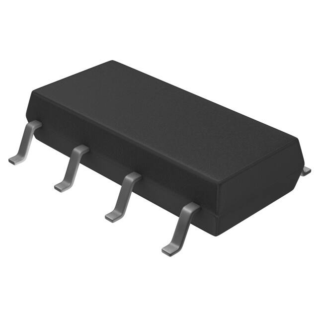
• Small and surface mount package (SOP-8)
• Pb-free and Halogen free
SOP-8
Ordering Information
Part No.
LEAD PLATING
μ PA2737GR-E1-AX
μ PA2737GR-E2-AX
Ni / Pd / Au
PACKING
Package
SOP-8
0.085 g TYP.
Tape 2500 p/reel
Absolute Maximum Ratings (TA = 25°C)
Item
Drain to Source Voltage (VGS = 0 V)
Gate to Source Voltage (VDS = 0 V)
Drain Current (DC)
Drain Current (pulse) ∗1
Total Power Dissipation ∗2
Total Power Dissipation (PW = 10 sec) ∗2
Channel Temperature
Symbol
VDSS
VGSS
ID(DC)
ID(pulse)
PT1
PT2
Tch
Storage Temperature
Single Avalanche Current ∗3
Single Avalanche Energy ∗3
Tstg
IAS
EAS
Ratings
−30
m20
m11
m110
1.1
2.5
150
Unit
V
V
A
A
W
W
°C
−55 to +150
11
12.1
°C
A
mJ
Thermal Resistance
Channel to Ambient Thermal Resistance ∗2
Rth(ch-A)
114
°C/W
Notes: ∗1. PW ≤ 10 μs, Duty Cycle ≤ 1%
∗
2. Mounted on a glass epoxy board of 25.4 mm x 25.4 mm x 0.8 mmt
∗
3. Starting Tch = 25°C, VDD = −15 V, RG = 25 Ω, VGS = −20 → 0 V, L = 100 μH
R07DS1317EJ0100 Rev.1.00
Jan 12, 2016
Page 1 of 6
�μPA2737GR
Electrical Characteristics (TA = 25°C)
Item
Zero Gate Voltage Drain Current
Symbol
IDSS
Gate Leakage Current
Gate Cut-off Voltage
Forward Transfer Admittance ∗1
IGSS
VGS(off)
| yfs |
Drain to Source On-state
Resistance ∗1
Input Capacitance
Output Capacitance
Reverse Transfer Capacitance
Turn-on Delay Time
Rise Time
Turn-off Delay Time
Fall Time
Total Gate Charge
Gate to Source Charge
Gate to Drain Charge
Body Diode Forward Voltage ∗1
Reverse Recovery Time
RDS(on)1
RDS(on)2
Ciss
Coss
Crss
td(on)
tr
td(off)
tf
QG
QGS
QGD
VF(S-D)
trr
Reverse Recovery Charge
Qrr
MIN.
TYP.
−1.0
4.5
MAX.
−1
Unit
μA
Test Conditions
VDS = −30 V, VGS = 0 V
m100
−2.5
nA
V
S
mΩ
mΩ
pF
pF
pF
ns
ns
ns
ns
nC
nC
nC
V
ns
VGS = m20 V, VDS = 0 V
VDS = −10 V, ID = −1 mA
VDS = −10 V, ID = −5.5 A
VGS = −10 V, ID = −11 A
VGS = −4.5 V, ID = −11 A
VDS = −10 V,
VGS = 0 V,
f = 1 MHz
VDD = −15 V, ID = −5.5 A,
VGS = −10 V,
nC
di/dt = 100 A/μs
9.7
17
1750
850
770
20
32
70
55
45
2.5
23
0.85
49
13
25
48
RG = 10 Ω
VDD = −24 V,
VGS = −10 V,
ID = −11 A
IF = 11 A, VGS = 0 V
IF = 11 A, VGS = 0 V,
Note: ∗1. Pulsed
TEST CIRCUIT 1 AVALANCHE CAPABILITY
TEST CIRCUIT 2 SWITCHING TIME
D.U.T.
RG = 25 Ω
D.U.T.
L
RL
50 Ω
PG.
VGS = −20 → 0 V
VDD
RG
PG.
VGS(−)
VGS
Wave Form
0
90%
VGS
10%
VDD
VDS(−)
−
IAS
BVDSS
VDS
ID
VGS(−)
0
VDS
Wave Form
τ
VDD
Starting Tch
τ = 1 μs
Duty Cycle ≤ 1%
VDS
90%
90%
10% 10%
0
td(on)
tr td(off)
ton
tf
toff
TEST CIRCUIT 3 GATE CHARGE
D.U.T.
PG.
IG = −2 mA
RL
50 Ω
VDD
R07DS1317EJ0100 Rev.1.00
Jan 12, 2016
Page 2 of 6
�μPA2737GR
TYPICAL CHARACTERISTICS (TA = 25°C)
FORWARD BIAS SAFE OPERATING AREA
DERATING FACTOR OF FORWARD BIAS SAFE
OPERATING AREA
-1000
30 ms
100 ms
ID(pulse) = –110 A
120
ID - Drain Current - A
-100
100
80
60
40
PW
ID(DC) = –11 A
-10
o
S(
-1
50
75
100
125
150
-0.01
-0.01
175
d
ite
L im
V
10
)
Po
we
r
D
=
10
0
s
DC
is
si
pa
tio
n
Li
Single Pulse
m
ite
d
TA = 25°C
Mounted on glass epoxy board of
25.4 mm x 25.4 mm x 0.8 mmt
-0.1
0
25
n)
R D S=
G
(V
20
0
10
ms
1m
s
μ
dT - Percentage of Rated Power - %
140
-0.1
-1
-10
-100
VDS - Drain to Source Voltage – V
TA - Ambient Temperature - °C
rth(t) - Transient Thermal Resistance - °C/W
TRANSIENT THERMAL RESISTANCE vs. PULSE WIDTH
1000
Rth(ch-A) = 114°C/W
100
10
1
0.1
Rth(ch-A):Mounted on glass epoxy board of
25.4 mm x 25.4 mm x 0.8 mmt
Single pulse
0.01
100 μ
1m
10 m
100 m
1
10
100
1000
PW - Pulse Width - s
DRAIN CURRENT vs.
FORWARD TRANSFER CHARACTERISTICS
DRAIN TO SOURCE VOLTAGE
-120
-100
TA = 150°C
75°C
25°C
–55°C
-10
V GS = –10 V
-80
-60
ID - Drain Current - A
ID - Drain Current - A
-100
–4.5 V
-40
-20
Pulsed
-0.5
-1
VDS - Drain to Source Voltage - V
R07DS1317EJ0100 Rev.1.00
Jan 12, 2016
-0.1
-0.01
Pulsed
VDS = –10 V
-0.001
-0
-0
-1
-1.5
-0
-1
-2
-3
-4
VGS - Gate to Source Voltage - V
Page 3 of 6
�GATE TO SOURCE CUT-OFF VOLTAGE vs.
FORWARD TRANSFER ADMITTANCE vs. DRAIN
CHANNEL TEMPERATURE
CURRENT
-2
-1
Pulsed
VDS = –10 V
ID = –1mA
-0
-50
RDS(on) - Drain to Source On-state Resistance - mΩ
| yfs | - Forward Transfer Admittance - S
-3
0
50
100
150
100
TA = 150°C
75°C
25°C
–55°C
10
1
Pulsed
VDS = –10 V
0.1
-0.01
-0.1
-1
-10
Tch - Channel Temperature - °C
ID - Drain Current - A
DRAIN TO SOURCE ON-STATE RESISTANCE vs.
DRAIN TO SOURCE ON-STATE RESISTANCE vs.
DRAIN CURRENT
GATE TO SOURCE VOLTAGE
40
Pulsed
30
VGS = –4.5 V
20
10
–10 V
0
-1
-10
-100
-1000
ID - Drain Current - A
RDS(on) - Drain to Source On-state Resistance - mΩ
VGS(off) – Gate to Source Cut-off Voltage - V
μPA2737GR
30
Pulsed
ID = –11 A
25
20
15
10
5
0
-0
-5
-10
-15
-20
VGS - Gate to Source Voltage - V
CAPACITANCE vs. DRAIN TO SOURCE VOLTAGE
DRAIN TO SOURCE ON-STATE RESISTANCE vs.
25
10000
Pulsed
ID = –11 A
20
Ciss, Coss, Crss - Capacitance - pF
RDS(on) - Drain to Source On-state Resistance - mΩ
CHANNEL TEMPERATURE
VGS = –4.5 V
15
10
VGS = –10 V
5
0
Ciss
1000
Coss
Crss
VGS = 0 V
f = 1 MHz
100
-50
0
50
100
Tch - Channel Temperature - °C
R07DS1317EJ0100 Rev.1.00
Jan 12, 2016
150
-0.1
-1
-10
-100
VDS - Drain to Source Voltage - V
Page 4 of 6
�μPA2737GR
DYNAMIC INPUT/OUTPUT CHARACTERISTICS
-10
-8
VGS
VDS
-15
-6
-10
-4
-5
-2
ID = –11 A
-0
-0
0
10
20
30
40
QG - Gate Charge - nC
R07DS1317EJ0100 Rev.1.00
Jan 12, 2016
50
IF - Diode Forward Current - A
VDD = –24V
–12V
–6V
-20
1000
VGS - Gate to Source Voltage - V
VDS - Drain to Source Voltage - V
-25
SOURCE TO DRAIN DIODE FORWARD VOLTAGE
100
VGS = –10 V
10
–4.5 V
0V
Pulsed
1
0
0.2
0.4
0.6
0.8
1
1.2
1.4
VF(S-D) - Source to Drain Voltage - V
Page 5 of 6
�μPA2737GR
Package Drawings (Unit: mm)
SOP-8
Equivalent Circuit
Drain
Body
Diode
Gate
Source
Remark
1, 2, 3
Source
4
Gate
5, 6, 7, 8 Darin
Strong electric field, when exposed to this device, can cause destruction of the gate oxide and
ultimately degrade the device operation. Steps must be taken to stop generation of static
electricity as much as possible, and quickly dissipate it once, when it has occurred.
R07DS1317EJ0100 Rev.1.00
Jan 12, 2016
Page 6 of 6
�Notice
1.
Descriptions of circuits, software and other related information in this document are provided only to illustrate the operation of semiconductor products and application examples. You are fully responsible for
the incorporation of these circuits, software, and information in the design of your equipment. Renesas Electronics assumes no responsibility for any losses incurred by you or third parties arising from the
use of these circuits, software, or information.
2.
Renesas Electronics has used reasonable care in preparing the information included in this document, but Renesas Electronics does not warrant that such information is error free. Renesas Electronics
3.
Renesas Electronics does not assume any liability for infringement of patents, copyrights, or other intellectual property rights of third parties by or arising from the use of Renesas Electronics products or
assumes no liability whatsoever for any damages incurred by you resulting from errors in or omissions from the information included herein.
technical information described in this document. No license, express, implied or otherwise, is granted hereby under any patents, copyrights or other intellectual property rights of Renesas Electronics or
others.
4.
You should not alter, modify, copy, or otherwise misappropriate any Renesas Electronics product, whether in whole or in part. Renesas Electronics assumes no responsibility for any losses incurred by you or
5.
Renesas Electronics products are classified according to the following two quality grades: "Standard" and "High Quality". The recommended applications for each Renesas Electronics product depends on
third parties arising from such alteration, modification, copy or otherwise misappropriation of Renesas Electronics product.
the product's quality grade, as indicated below.
"Standard": Computers; office equipment; communications equipment; test and measurement equipment; audio and visual equipment; home electronic appliances; machine tools; personal electronic
equipment; and industrial robots etc.
"High Quality": Transportation equipment (automobiles, trains, ships, etc.); traffic control systems; anti-disaster systems; anti-crime systems; and safety equipment etc.
Renesas Electronics products are neither intended nor authorized for use in products or systems that may pose a direct threat to human life or bodily injury (artificial life support devices or systems, surgical
implantations etc.), or may cause serious property damages (nuclear reactor control systems, military equipment etc.). You must check the quality grade of each Renesas Electronics product before using it
in a particular application. You may not use any Renesas Electronics product for any application for which it is not intended. Renesas Electronics shall not be in any way liable for any damages or losses
incurred by you or third parties arising from the use of any Renesas Electronics product for which the product is not intended by Renesas Electronics.
6.
You should use the Renesas Electronics products described in this document within the range specified by Renesas Electronics, especially with respect to the maximum rating, operating supply voltage
range, movement power voltage range, heat radiation characteristics, installation and other product characteristics. Renesas Electronics shall have no liability for malfunctions or damages arising out of the
use of Renesas Electronics products beyond such specified ranges.
7.
Although Renesas Electronics endeavors to improve the quality and reliability of its products, semiconductor products have specific characteristics such as the occurrence of failure at a certain rate and
malfunctions under certain use conditions. Further, Renesas Electronics products are not subject to radiation resistance design. Please be sure to implement safety measures to guard them against the
possibility of physical injury, and injury or damage caused by fire in the event of the failure of a Renesas Electronics product, such as safety design for hardware and software including but not limited to
redundancy, fire control and malfunction prevention, appropriate treatment for aging degradation or any other appropriate measures. Because the evaluation of microcomputer software alone is very difficult,
please evaluate the safety of the final products or systems manufactured by you.
8.
Please contact a Renesas Electronics sales office for details as to environmental matters such as the environmental compatibility of each Renesas Electronics product. Please use Renesas Electronics
products in compliance with all applicable laws and regulations that regulate the inclusion or use of controlled substances, including without limitation, the EU RoHS Directive. Renesas Electronics assumes
no liability for damages or losses occurring as a result of your noncompliance with applicable laws and regulations.
9.
Renesas Electronics products and technology may not be used for or incorporated into any products or systems whose manufacture, use, or sale is prohibited under any applicable domestic or foreign laws or
regulations. You should not use Renesas Electronics products or technology described in this document for any purpose relating to military applications or use by the military, including but not limited to the
development of weapons of mass destruction. When exporting the Renesas Electronics products or technology described in this document, you should comply with the applicable export control laws and
regulations and follow the procedures required by such laws and regulations.
10. It is the responsibility of the buyer or distributor of Renesas Electronics products, who distributes, disposes of, or otherwise places the product with a third party, to notify such third party in advance of the
contents and conditions set forth in this document, Renesas Electronics assumes no responsibility for any losses incurred by you or third parties as a result of unauthorized use of Renesas Electronics
products.
11. This document may not be reproduced or duplicated in any form, in whole or in part, without prior written consent of Renesas Electronics.
12. Please contact a Renesas Electronics sales office if you have any questions regarding the information contained in this document or Renesas Electronics products, or if you have any other inquiries.
(Note 1)
"Renesas Electronics" as used in this document means Renesas Electronics Corporation and also includes its majority-owned subsidiaries.
(Note 2)
"Renesas Electronics product(s)" means any product developed or manufactured by or for Renesas Electronics.
http://www.renesas.com
SALES OFFICES
Refer to "http://www.renesas.com/" for the latest and detailed information.
Renesas Electronics America Inc.
2801 Scott Boulevard Santa Clara, CA 95050-2549, U.S.A.
Tel: +1-408-588-6000, Fax: +1-408-588-6130
Renesas Electronics Canada Limited
9251 Yonge Street, Suite 8309 Richmond Hill, Ontario Canada L4C 9T3
Tel: +1-905-237-2004
Renesas Electronics Europe Limited
Dukes Meadow, Millboard Road, Bourne End, Buckinghamshire, SL8 5FH, U.K
Tel: +44-1628-585-100, Fax: +44-1628-585-900
Renesas Electronics Europe GmbH
Arcadiastrasse 10, 40472 Düsseldorf, Germany
Tel: +49-211-6503-0, Fax: +49-211-6503-1327
Renesas Electronics (China) Co., Ltd.
Room 1709, Quantum Plaza, No.27 ZhiChunLu Haidian District, Beijing 100191, P.R.China
Tel: +86-10-8235-1155, Fax: +86-10-8235-7679
Renesas Electronics (Shanghai) Co., Ltd.
Unit 301, Tower A, Central Towers, 555 Langao Road, Putuo District, Shanghai, P. R. China 200333
Tel: +86-21-2226-0888, Fax: +86-21-2226-0999
Renesas Electronics Hong Kong Limited
Unit 1601-1611, 16/F., Tower 2, Grand Century Place, 193 Prince Edward Road West, Mongkok, Kowloon, Hong Kong
Tel: +852-2265-6688, Fax: +852 2886-9022
Renesas Electronics Taiwan Co., Ltd.
13F, No. 363, Fu Shing North Road, Taipei 10543, Taiwan
Tel: +886-2-8175-9600, Fax: +886 2-8175-9670
Renesas Electronics Singapore Pte. Ltd.
80 Bendemeer Road, Unit #06-02 Hyflux Innovation Centre, Singapore 339949
Tel: +65-6213-0200, Fax: +65-6213-0300
Renesas Electronics Malaysia Sdn.Bhd.
Unit 1207, Block B, Menara Amcorp, Amcorp Trade Centre, No. 18, Jln Persiaran Barat, 46050 Petaling Jaya, Selangor Darul Ehsan, Malaysia
Tel: +60-3-7955-9390, Fax: +60-3-7955-9510
Renesas Electronics India Pvt. Ltd.
No.777C, 100 Feet Road, HAL II Stage, Indiranagar, Bangalore, India
Tel: +91-80-67208700, Fax: +91-80-67208777
Renesas Electronics Korea Co., Ltd.
12F., 234 Teheran-ro, Gangnam-Gu, Seoul, 135-080, Korea
Tel: +82-2-558-3737, Fax: +82-2-558-5141
© 2016 Renesas Electronics Corporation. All rights reserved.
Colophon 5.0
�